What Is a Blank PCB Called?
A blank PCB is commonly referred to as a bare board. This term is used because the board has no components soldered onto it yet. It’s simply the foundation of a printed circuit board (PCB), typically made from a material like fiberglass and copper. The copper traces on the board outline where the electrical connections will eventually be made, but before any components are attached, the board remains “blank.”
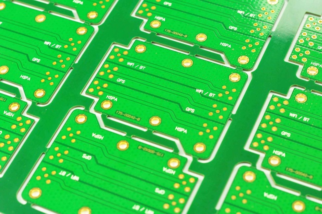
A bare board is key point in the manufacturing process of electronic devices. Once components like resistors, capacitors, and integrated circuits are added, the blank PCB transforms into a fully functional circuit board. This is the stage where the blank board evolves, moving from raw material to the heart of a functioning device.
How to Use a Blank PCB Board?
Using a blank PCB starts with designing a circuit schematic. Specialized software is used to create a layout that specifies where each component will be placed and how they’ll be connected through copper traces. Once the design is finalized, the blank board serves as a canvas where components are either soldered by hand or using automated machines in mass production.
If you are working on a DIY project or prototyping, the blank PCB allows for customization and flexibility. You can use a soldering iron to manually attach your components. For large-scale production, automated machines place and solder components onto the blank board with precision. Using blank PCBs for custom designs or modifications is a cost-effective way to experiment with electronics.
Why Is PCB So Cheap?
PCBs are considered affordable due to mass production techniques. Modern manufacturing processes, such as automated assembly lines and the use of standard materials, have significantly reduced costs. The global nature of the electronics industry also plays a role, as many manufacturers source materials and labor from countries with lower production costs.
The materials used, primarily fiberglass and copper, are relatively inexpensive. Furthermore, technological advancements have optimized the process of making PCBs, allowing manufacturers to produce them quickly and in large quantities. The result is that even highly specialized PCBs can be produced at a low cost, making them accessible to hobbyists, startups, and large corporations alike. If you want to know the details about factors affect the price of PCB board, welcome to check our another blog:
How Are Blank PCBs Made?
The process of making blank PCBs is a sophisticated, multi-stage operation that ensures the boards meet high precision standards before any components are added. Here’s a detailed breakdown of the steps involved in manufacturing a blank PCB:
- Material Selection and Lamination
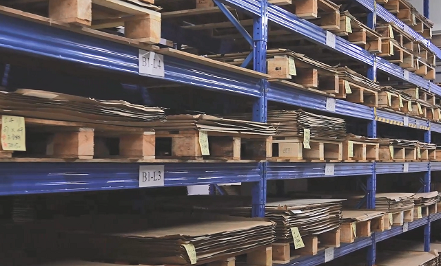
Blank PCBs start with a substrate, typically made from fiberglass-reinforced epoxy laminate (FR4), which serves as the board’s structural foundation. This substrate is non-conductive, providing insulation for the circuit. A copper layer is then bonded to one or both sides of the substrate using heat and pressure, forming what is known as a copper-clad laminate. The thickness of this copper layer varies based on the board’s intended application, with typical copper thickness ranging from 1 oz (35 µm) to 2 oz (70 µm) per square foot. Thicker copper layers may be used for boards handling higher currents.
- Photoresist Application
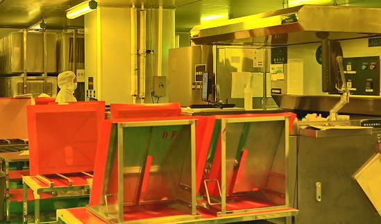
After lamination, the copper layer is coated with a light-sensitive material called photoresist. This step prepares the board for the next process, which is exposing the circuit pattern. The photoresist layer can be either liquid or dry film and plays a critical role in protecting certain parts of the copper during etching.
- Imaging the Circuit Pattern
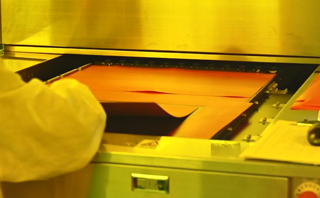
The desired circuit pattern, generated from PCB design software, is transferred onto the board. This is done by aligning the photoresist-coated board with a photomask (a stencil-like film) that contains the circuit layout. The board is then exposed to ultraviolet (UV) light. The areas of the photoresist not covered by the photomask are hardened, while the areas shielded by the mask remain soft and will later be removed.
- Etching Process
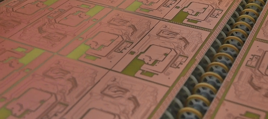
The next step is to remove the unneeded copper from the board, a process called etching. Chemical etchants, like ferric chloride or ammonium persulfate, are used to dissolve the unprotected copper, leaving behind only the circuit traces. The areas of the copper protected by the hardened photoresist remain intact, forming the conductive pathways for the future components.
- Drilling Holes for Components
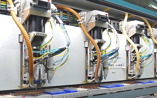
After the etching process, holes need to be drilled into the board. These holes, called vias, allow for the placement of components such as resistors, capacitors, and integrated circuits, and are also used to connect different layers in multi-layer PCBs. Advanced PCB manufacturing often uses computer numerical control (CNC) drilling machines to ensure precision, especially for boards with many layers or small trace designs. Some manufacturers employ laser drilling for microvias.
- Plating and Hole Metallization
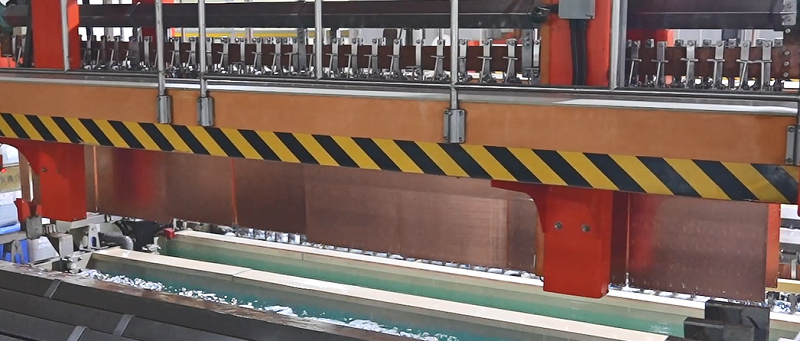
Once the holes are drilled, they need to be plated to create electrical connections between the different layers of the PCB. This is done through a process called electroless copper plating, which deposits a thin layer of copper inside the drilled holes. The plating process ensures that when components are later inserted, electrical signals can flow between layers through the plated holes.
- Solder Mask
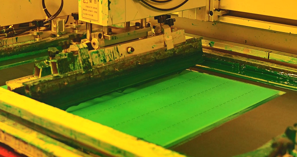
After drilling and plating, the board is cleaned and coated with a layer of solder mask. This mask protects the copper traces and prevents solder from accidentally bridging across traces during assembly. The solder mask is typically green, though other colors like blue, red, black, or white can also be used. The solder mask is applied through a screen-printing process or as a dry film, and it is cured using UV light or heat.
- Silkscreen Printing
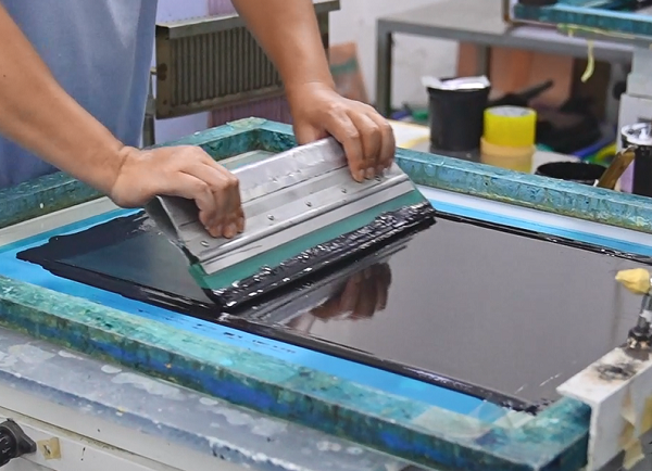
Silkscreen printing is applied to the board to mark component locations, symbols, logos, or other identifiers needed during the assembly process. This layer is typically applied using a silk-screening process, similar to how images are printed onto clothing. White is the most common color used for silkscreen, as it provides high contrast against the green solder mask, but other colors can be used depending on the design.
- Surface Finishing
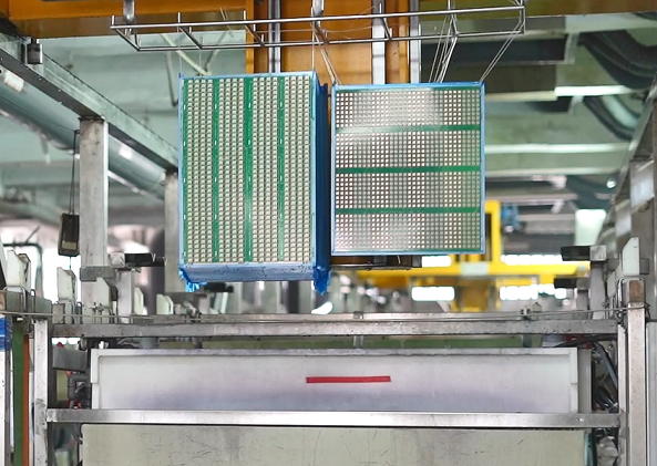
The copper pads, where components will be soldered later, are treated with a surface finish to protect them from oxidation and ensure good solderability. Common finishes include HASL (Hot Air Solder Leveling), where the board is dipped in molten solder and excess solder is blown off with hot air, leaving a smooth surface. Another popular finish is ENIG (Electroless Nickel Immersion Gold), where a thin layer of nickel followed by gold is applied to the copper pads.
- Electrical Testing and Quality Control
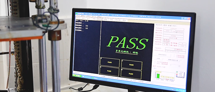
The final step in producing a blank PCB is electrical testing and quality control. Every trace and connection is tested to ensure there are no shorts or opens, which could render the board useless. Automated Optical Inspection (AOI) systems are used to visually inspect the board for defects, while flying probe tests and bed-of-nails tests check for electrical continuity. Any defects found at this stage are flagged for repair or, in severe cases, the board is scrapped.
What Is the Difference Between Bare PCB and PCB?
The term bare PCB refers to the unpopulated circuit board, which means it lacks any electronic components. In contrast, a PCB refers to a fully assembled board that includes all the necessary components to function.
In the bare stage, the PCB is simply the foundation for the circuit but isn’t functional. Once components are soldered onto the bare PCB, it becomes an operational printed circuit board, ready to be integrated into electronic devices.
How Do You Cut Blank PCB?
Cutting a blank PCB requires precision. Tools such as PCB shears, laser cutters, or CNC machines are commonly used to achieve clean, straight cuts without damaging the copper traces. For smaller DIY projects, a hand saw or scoring tool can be used, but these methods require a steady hand and careful planning to avoid mistakes.
Before cutting, it’s important to mark the board clearly to ensure the cuts are accurate. If the board is part of a larger project, cutting should be done after confirming that all components will fit within the intended space.
Why Are PCBs Green?
The green color on most PCBs comes from the solder mask that coats the board. While green is the most common color, the solder mask can be found in other colors such as red, blue, or black. The preference for green is largely historical, as it provided the best contrast for technicians to inspect the board visually.
Green solder masks also tend to offer better performance under different lighting conditions, which can be helpful during manufacturing and quality control processes.
Do PCBs Use AC or DC?
PCBs can handle both AC (alternating current) and DC (direct current), depending on the design and the type of components used. Some boards are designed specifically for DC circuits, while others are built to handle AC power.
For example, a power supply PCB may convert AC from a wall outlet into DC, which is used by many electronic devices. The flexibility to work with either type of current makes PCBs essential for a wide range of applications.
Blank PCB Board Supplier – EBest Circuit (Best Technology)
With over 18 years as an industry leader, EBest Circuit (Best Technology) is one of the most experienced PCB and PCB assembly manufacturer in Asia. We are highly specialized not only in quick-turn PCB prototype and PCB assembly, but also medium and small volume PCB fabrication. In EBest Circuit (Best Technology), you can enjoy a full-comprehensive one-stop service from PCB design, layout, PCB fabricate, PCB assembly, function testing and delivery. We always try our best to fabricate your PCB with copper clad laminate with the highest quality to meet your demands.
If you have any questions, please feel free to contact us with sales@bestpcbs.com, we will be happy to help you.
Tags: blank pcb


