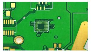
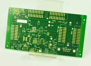
Laser direct imaging (LDI) technology is a process that uses lasers to expose images directly on photoresists, mainly used in the exposure process of PCB manufacturing processes. LDI is a widely used technology that can create a variety of images and is used in various industries, including electronics, automotive and medical industries.
What is laser direct imaging?
Laser direct imaging (LDI) is an advanced photolithography technology. It directly uses a laser beam to expose images on photoresists, eliminating the intermediate step of making photolithography masks in traditional photolithography technology.
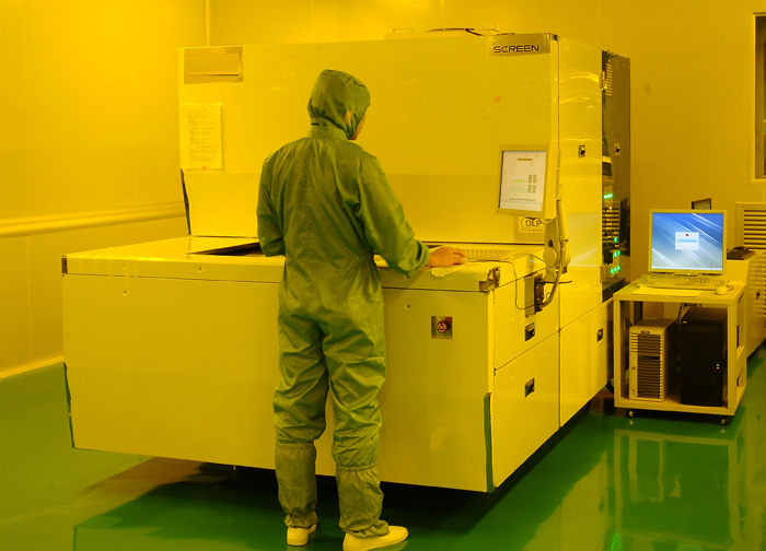
In this process, the laser beam is precisely controlled according to the pre-set circuit pattern data. The laser emitted by the laser light source is processed by a series of optical components, such as beam expansion and focusing, and then the laser beam is guided by the scanning system to scan and expose the surface of the printed circuit board (PCB) coated with photoresist.
The photoresist responds to the laser energy, and according to the type of photoresist (positive or negative), the corresponding chemical changes occur in the laser irradiation area. This change will lay the foundation for subsequent development and other processes, thereby forming an accurate circuit pattern.
What is the principle of laser direct imaging?
The principle of laser direct imaging (LDI) is to expose the pattern directly on the substrate coated with photosensitive material through a computer-controlled laser beam.
Specifically, the workflow of LDI includes the following steps: First, the designed circuit pattern is converted into the image generation program of the spatial light modulator through computer-aided manufacturing (CAM) software. Then, the laser beam passes through the spatial light modulator, and the generated image is projected onto the substrate coated with photosensitive material through the optical imaging system to complete the pattern exposure. Compared with the traditional mask exposure process, LDI saves the film process in the exposure process and greatly improves the production efficiency.
The main advantages of LDI technology are its efficiency and precision. It directly uses a highly focused laser beam controlled by a computer to define the circuit pattern on the PCB copper layer covered with laser photoresist without the need for photographic tools, thus avoiding the film and printing defects in the traditional process.
In addition, LDI also optimizes the production environment, eliminates the influence of temperature and humidity on the product, and further improves the production quality and efficiency.
How does laser direct imaging (LDI) work?
Laser direct imaging (LDI) technology is a process that uses laser to directly expose and image on photoresist, and is mainly used in the exposure process in the PCB manufacturing process. Its working principle is as follows:
- 1. Design graphics: Design the circuit graphics to be produced through computer-aided design (CAD) software.
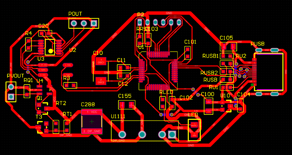
- 2. Generate images: Convert the designed circuit graphics into digital images and transmit them to the control system of the LDI equipment.
- 3. Laser scanning: The laser beam in the LDI equipment scans and exposes the photoresist according to the information of the digital image under the precise control of the control system.
- 4. Photochemical reaction: The photoresist undergoes a photochemical reaction under the irradiation of the laser, changing its solubility.
- 5. Development: The exposed photoresist is developed in the developer to remove the unexposed part of the photoresist, thereby forming a circuit pattern on the photoresist that is consistent with the design graphics.
- 6. Etching or electroplating: According to needs, the developed circuit board is etched or electroplated and other subsequent processes are performed to produce the actual circuit.
Compared with traditional exposure technology, LDI technology has higher resolution and precision, can produce finer circuit wiring and smaller line spacing, and also has higher production efficiency and flexibility.
What are the advantages of using laser direct imaging?
The main advantages of LDI (Laser Direct Image) technology include: eliminating the film process in the exposure process, saving time and cost for loading and unloading films, and reducing deviations caused by film expansion and contraction; directly imaging CAM data on PCB, eliminating CAM production process; high image resolution, fine wires can reach about 20um, suitable for fine wire production; improve PCB production yield.
The main problems of LDI technology include: high-precision lasers and optical systems are required, which increases the cost and complexity of the equipment; high environmental requirements, temperature and humidity need to be controlled to ensure imaging quality; high technical requirements for operators, and professional training is required to operate the equipment proficiently.
The advantages of LDI technology in the flexible board industry include: improving production efficiency, no need to make and replace physical masks, shortening production cycles and waiting time; high-precision imaging, capable of processing finer and more complex graphics, improving product yield and reliability; efficient use of materials, reducing material waste; environmental advantages, reducing the use of chemicals, and reducing environmental pollution.
What are the disadvantages of laser direct imaging?
The disadvantages of laser direct imaging (LDI) technology mainly include:
- 1. High equipment cost: LDI equipment is usually expensive and requires a large initial investment, which may be a burden for some small enterprises or projects.
- 2. High environmental requirements: LDI equipment needs to work in a specific environment, such as a dark room or a low-illuminance red light environment, which increases the requirements for the working environment.
- 3. Technical complexity: LDI technology involves multiple steps and complex process flows, with high technical requirements for operators, and long training costs and time.
- 4. High material cost: LDI requires the use of specific photoresists and laser diodes, which are expensive and increase production costs.
- 5. Speckle problem: After the laser beam is reflected or transmitted through a rough surface, it will form countless independent scattered sub-waves. These sub-waves are coherently superimposed during the spatial propagation process, forming random and irregularly distributed bright and dark spots in space, that is, speckle phenomenon, which may affect the imaging quality.
In summary, although LDI technology has the advantages of high precision and high efficiency, its disadvantages such as high equipment cost, complex technical requirements and speckle problem also need to be considered when using it.
When is laser direct imaging used?
Laser direct imaging LDI is mainly used in the exposure process in PCB manufacturing, especially when high precision and efficient production are required. This technology is particularly suitable for the production of fine-line and ultra-fine-line circuit boards, and can achieve the best imaging effect.
In addition, LDI technology is also widely used in the field of FPC soft boards, which can improve production efficiency and product quality, and support complex circuit structures and high-density layouts.
The advantages of laser direct imaging LDI technology include:
- 1. High precision: It can achieve high-resolution pattern exposure and improve product performance and reliability.
- 2. Efficient production: shorten the exposure process, speed up production and reduce costs.
- 3. Complex circuit structure: support the exposure of multi-layer FPC and meet the needs of high-density layout.
Laser direct imaging technology is a highly promising technology in the field of PCB manufacturing. It has many advantages in terms of precision, flexibility, production efficiency and cost-effectiveness, and plays an important role in PCB manufacturing in many fields such as high-end electronic products, automotive electronics, industrial control and communication equipment.
Tags: laser direct imaging, PCB, PCB technology


