During the PCB board manufacturing, there is an important process called surface treatment. This is mainly used to protect the board surface from oxidation, corrosion, and good electricity. Gold plating, also is a popular surface finishing method, which commonly used in the industry. As a professional PCB fabricator, here Best Team would like to introduce some key points about gold plating that customers always pay more attention to. Let’s keep reading!
What is Gold Plating in PCB?
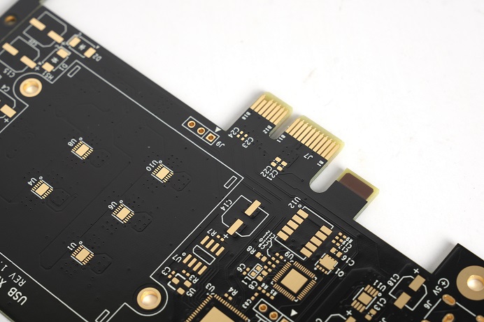
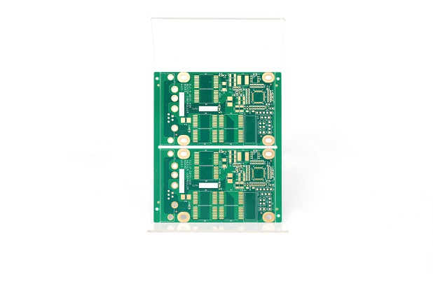
Firstly, let’s know what is a gold plating. Gold plating on PCBs refers to a layer of gold applied over specific areas of a circuit board. This gold coating is typically applied on the connectors, pads, and edge contacts of a PCB to improve electrical conductivity and provide better resistance against wear and oxidation. Gold plating protects these sensitive areas, which are critical for the performance and reliability of the PCB.
The principle of gold plating is to dissolve nickel and gold (commonly known as gold salt) in the chemical solution. And then the circuit board is immersed in the electroplating cylinder and the current is passed on the copper foil surface of the circuit board to generate nickel gold coating. Due to the electric nickel gold has good hardness, wear resistance, and not easy to oxidization, it is widely used in the electronics.
Does Gold Plating Process Use Real Gold?
The gold plating in PCB is not really pure gold, but a gold alloy (has gold and some other metals in it).
In PCB manufacturing, gold-plating is usually not done using pure gold, but by compression and treatment of gold alloys. Such alloys often contain small amounts of metals such as silver, nickel, and copper to reduce costs and meet specific performance requirements.
The role of gold plating in PCB is mainly to enhance electrical conductivity and chemical stability. Gold has good electrical conductivity and oxidation resistance, which can provide stable signal transmission and reliable connections in electronic devices. In addition, gold does not discolor or corrode, making it an ideal material for electronic applications.
In general, there are two main gold-plating processes: electrolytic gold-plating and brush gold-plating. Electrolytic gold plating is the deposition of metal on the circuit board through chemical bath and electrolytic process, which has higher cost but better quality. Brush gold plating, by depositing metal particles onto a conductive substrate via electronic devices, is cheaper but of poorer quality.
Why Use Gold in PCB?
May somebody curious about why use gold in PCB? To make the PCB surface more beautiful? Let me tell you why.
1. Improve electrical conductivity
Metals such as gold have good electrical conductivity. Through gold plating, a metal conductive layer can be formed at the circuit connection of the PCB board, thus significantly improving the electrical conductivity of the circuit. This helps to reduce the resistance at the circuit connection, reduce signal loss.
2. Prevent oxidation and corrosion
The gold coating has excellent chemical stability and can resist oxidation and corrosion. This can protect the PCB board from the erosion of harmful substances in the external environment, such as humidity, salt spray, chemical gases, etc., thereby extending its service life.
3. Improve welding performance
Oxidized layer may be formed on the metal surface during welding, affecting welding quality. The gold coating can reduce the thickness of the surface oxide layer, thereby improving the reliability and robustness of the welding. In addition, gold plating can also provide better welding contact, reduce thermal stress during welding, and reduce the occurrence of welding defects.
4. Enhance the appearance
Gold plating can give the PCB surface metallic luster, improve the appearance texture and product grade, and increase the market competitiveness of the product. To be honest, gold appearance indeed gives a better appearance.
5. Meet specific needs
In some high-end electronic products, there are higher requirements for the electrical conductivity, corrosion resistance, welding performance and appearance texture of PCB boards. Gold plating, as an effective surface treatment technology, can meet these specific needs.
6. Meet welding quality challenges
With the improvement of integration of electronic products, IC feet are becoming more and more dense, and traditional vertical tin injection technology is difficult to meet the welding challenges of thin pads. Gold plating technology can provide better welding performance and reliability, and reduce the occurrence of welding quality problems such as virtual welding.
How Thick is Gold Plating on Circuit Boards?
The thickness of gold plating on PCBs depends on the type and application. Generally, PCB gold plating thickness ranges from 0.1-1.27um. For standard PCBs, a gold layer thickness of 0.03 to 0.05 microns is common, especially for immersion gold. However, thicker plating is applied for connectors or contacts exposed to frequent wear and tear, as these areas need more protection.
Hard gold, used for high-wear applications like edge connectors, typically has a greater thickness than immersion gold. The thickness is carefully controlled because too thin a layer might fail to provide effective protection, while an excessively thick layer could lead to wasted materials and unnecessary expense. The goal is to strike a balance that delivers durability without incurring excessive costs.
What is the Difference Between Immersion Gold and Hard Gold PCB?
Hard gold plating is by electroplating, so that the gold particles are attached to the PCB board, so it is also called electric gold. Because of its strong adhesion, hard gold plating is also called hard gold, which is often used for memory bar gold finger and other parts that need wear-resistant.
Immersion gold is through the chemical reaction, the gold particles crystallization and attached to the PCB pad, so it is also known as soft gold. Due to the weak adhesion, the sinking gold is mainly used for the surface treatment of the pad, and the weldability is good. The difference between hard gold plating and immersion gold are including:
- Color: Immersion gold is more yellow, while gold plating is more white.
- Crystal structure: Immersion gold has a denser crystal structure.
- Thickness: Immersion gold has a thicker layer of gold.
- Wear resistance: Gold plating is harder and more resistant to wear and tear.
- Solderability: Immersion gold is easier to solder.
- Short circuits: Gold plating is more likely to cause short circuits.
- Oxidation resistance: Immersion gold is less prone to oxidation.
- Cost: Immersion gold is more expensive.
- Deposition process: Gold plating uses an external electric current, while immersion gold is a chemical process.
- Suitability: Gold plating is better for environments with high mechanical stress, while immersion gold is better for movable contacts.
PCB Applications of Gold Plating
Gold-plated PCBs are popular in industries where reliability and durability are essential. Some typical applications include:
- Aerospace and Defense
- Medical Devices
- Telecommunications
- Consumer Electronics
- High power electronics
- High current electronics
- Low voltage digital logic electronics
As a PCB and PCBA manufacturer, we provide various surface treatment options for customers, including: ENIG, ENEPIG, OSP, HASL-LF, Immersion gold, hard gold (up to 50u’’). We offer customized PCB service tailored to customer’s requirements, we will try our best to meet the demands of surface treatment. Welcome to contact us if you have any questions.
Tags: gold plated pcb board


