In the field of modern electronic manufacturing, high-density interconnect (HDI) technology has become a key factor driving the development of electronic products towards miniaturization and higher performance. The core of HDI technology lies in its unique stacked design, which not only greatly improves the space utilization of circuit boards, but also significantly enhances electrical performance and signal integrity.
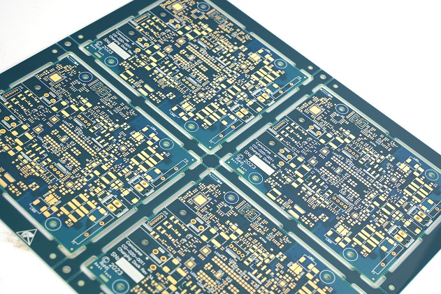
The stacked-up design of HDI PCB allows multiple circuit layers to be connected through precisely controlled blind and buried holes, which have much smaller diameters than traditional PCB through holes. This connect method not only reduces the volume of the circuit board, but also increases the trace density, so that more and more electronic components can be integrated into a limited space.
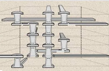
In addition, the stacked design of HDI also optimizes the path of signal transmission. Due to the shorter signal transmission distance and the avoidance of unnecessary bends and corners, signal delay and loss have been effectively controlled. This is crucial for high-speed electronic devices as they require fast and accurate processing of large amounts of data.
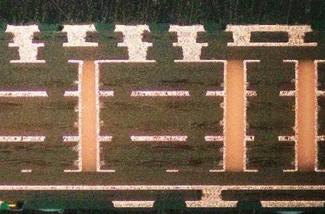
In the manufacturing process, the stacked design of HDI also brings many challenges. In order to achieve high-precision buried/blind hole machining and interlayer registration, manufacturers must adopt advanced laser drilling technology and precision etching equipment. At the same time, in order to ensure the reliability and stability of the circuit board, strictly testing and verification of materials and processes are also required.
So what are the HDI stacking structures? This article will take you into an incredibly wonderful world…
1+N+1 Stack Up
1. Here, “1” (including the following “1”) refers to the layer number of blind holes (Blind via/ micro-via). And one layer blind hole always called a first step.
N refers to the number of non-blind hole layers in the inner layer (not necessarily just the Core), such as 4 layers, combined with 1, which is a 1-4-1 stacked structure. At the same time, if the N-layer is laminated, then this 1-4-1 laminated structure is called first-step-second-lamination (1 times N-layer lamination + 1 times outer layer lamination = 2 times, so it is called second lamination).
Does it make sense? If you have any questions, feel freely to leave a message or contact us at sales@bestpcbs.com.
2. Typical 1+N+1 stack-up
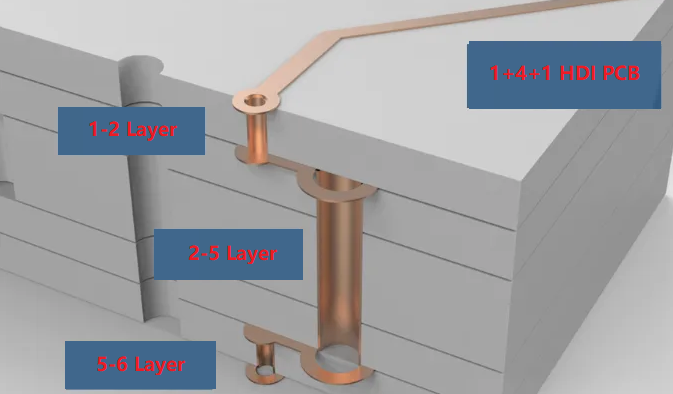
This kind of stack up shown as following is made by laminate a CCL sheet into 4 layers firstly and then laminate into 6 layers. It is also a common product on the market at present.
2+N+2 Stack Up
1. Here, 2 and N have the same meaning as 1-N-1, it will not be repeated again.
2. Typical 2+N+2 stack-up:
There are two types of second-step stack-up: stacked via and staggered via, which have different levels in difficulty, cost, and process.
2.1 Staggered via
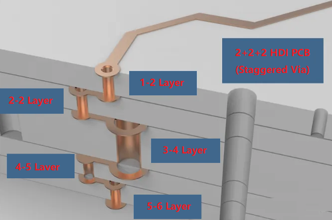
Here is a stack-up of a staggered vias, this kind of structure has relatively lower cost and good reliability.
2.2 Stacked via
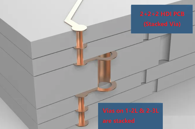
From the stack-up, it is not difficult to see the difference with staggered vias. This stacking structure requires drilling another blind hole on top of the blind hole, and the previous blind hole needs to be filled with copper or a material that can conduct electricity and resist laser drilling. This gives a rise to another technology, we will introduce in the later HDI electroplating process.
N+N Stack Up
1. Here, the “N” and the “N” in 1-N-1 or 2-N-2 have the same meaning.
2. Typical N+N stack-up
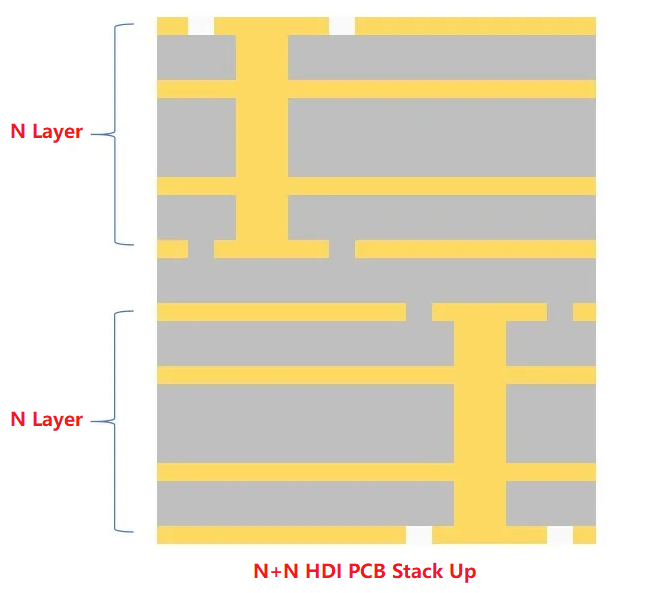
Although N+N stacking may not have blind holes, due to the special process and strict registration requirements, the actual production difficulty is no less than HDI technology.
Anylayer for Any Interconnection
1. The Any-layer means it can conduct at any layer, so how to achieve it?
2. Typical stack-up of Any-layer
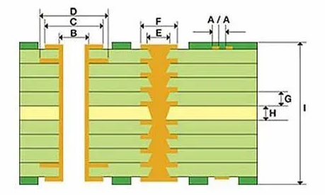
From the section of the PCB as following, it can also be seen that how to stack each layer together to form a straight line is also a challenge, so the Anylayer process good or not depends on the registration ability of the manufacturer. Of course, the circuit uses this technology will definitely be very dense and fine, which gives rise to an advanced PCB process called MSAP.
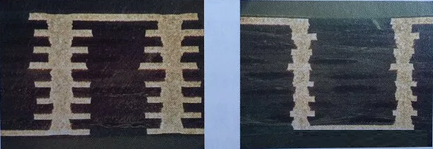
So in summary, despite facing many challenges, HDI’s stacked design has become a key part of high-end electronic products. From smartphones to wearable devices, from high-performance computers to advanced communication systems, HDI technology is playing a crucial role. With the continuous advancement of technology and the increasing demand from consumers, we have reason to believe that HDI’s stacking will continue to lead the innovation trend in the field of electronic manufacturing.
Tags: HDI PCB


