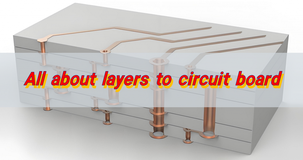
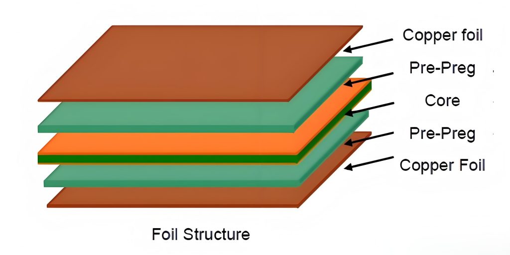
The layers to circuit board are essential for defining its structure and functionality. The substrate provides mechanical support; the conductive layer is responsible for signal transmission and power distribution; the insulating layer is placed between the conductive layers to prevent short circuits; the solder mask protects the circuit board and ensures reliable welding; the outermost screen printing layer is used for marking and guiding component placement.
How many layers does a circuit board have?
The number of layers of a circuit board can range from single to multiple layers. Common layers include single, double, four, six, eight, ten and twelve layers.
Single-layer boards are the most basic type of circuit boards. All components and circuits are on the same layer. The manufacturing cost is low but suitable for simple circuit designs.
Double-layer boards connect the upper and lower layers through vias and are suitable for medium-complex circuit designs.
Four-layer boards have two layers of internal copper foil, which have higher noise suppression and anti-interference capabilities and are often used in industrial control and communication fields.
Six-layer boards can optimize electromagnetic interference and are suitable for circuit designs that need to transmit signals at different speeds.
Eight-layer boards usually contain four wiring layers and four reference planes, which are suitable for high-end electronic devices and aerospace fields.
Common circuit board layers on the market include 1 layer, 2 layers, 4 layers, 6 layers, 8 layers, 10 layers and 12 layers. High-end PCB boards can even reach 32 layers or 50 layers, but these are usually used for special needs and high-performance equipment.
The number of layers of a circuit board has a significant impact on performance and cost. Multi-layer circuit boards have higher performance and reliability and can adapt to complex circuit design requirements, but the cost also increases with the number of layers.
What are the layers of a PCB layout?
PCB design includes multiple layers, each with its specific function:
- Signal layer: including Top Layer, Bottom Layer and Mid Layer, used to install components and routing.
- Mechanical layer: defines the appearance and mechanical size of the PCB board, without electrical properties, used to outline the shape, place text, etc.
- Silkscreen layer: including Top Overlay and Bottom Overlay, used to define silkscreen characters, such as component names, symbols, etc.
- Solder paste layer: including Top Paste and Bottom Paste, used for surface mount pads.
- Solder mask layer: including Top Solder and Bottom Solder, to prevent short circuit during soldering.
- Drilling layer: provides drilling information during manufacturing.
- Prohibited wiring layer: defines wiring boundaries to prevent wiring from exceeding the range.
- Multilayer: used for electrical connection of pads and vias.
Can a PCB have 3 layers?
PCB can have 3 layers. Three-layer PCB board does exist, which has a design with three copper layers, including two outer copper layers and one inner copper layer, and the inner copper layer is located between the two outer copper layers.
However, although three-layer PCB board is technically feasible, it is not common in practical applications. The main reasons include:
- The process cost difference is not big: the process cost of three-layer board and four-layer board is not much different, because the four-layer board has an extra layer of copper foil and adhesive layer, but this difference is not enough to significantly increase the cost.
- Process stability issues: In the PCB manufacturing process, four-layer boards are easier to control than three-layer boards, especially in terms of symmetry and warpage. Three-layer boards are prone to exceed this standard when they are large in size, affecting the reliability of SMT patches and the entire product.
- Design habits: Designers usually tend to design boards with even layers. Even if odd-numbered boards can achieve functions, they will be designed as even layers to avoid potential problems.
How do you tell how many layers a PCB is?
The methods for judging the number of PCB layers mainly include the following:
1. Appearance judgment method:
- Observation of copper foil layer: A single-layer PCB board has only one copper foil layer, one side of the double-sided component has copper foil, and the other side is printed circuit. A double-layer PCB board has two copper foil layers, located on both sides of the board. Four-layer and six-layer PCB boards have more copper foil layers, and the thickness of the board increases accordingly.
- Drilling position and number: The drill holes in a multi-layer PCB board are channels connecting different layers. The drilling holes of double-layer PCBs are mostly located in the four corners, while four-layer or six-layer PCBs will have more drilling holes in the middle, and the drilling positions and quantities are more complicated.
- Board thickness: Generally, the thickness of single-sided copper PCBs is 1.6mm, the thickness of double-sided copper PCBs is 1.2-1.6mm, and the thickness of four-layer PCBs is 1.6~2.0mm. If the thickness of the PCB board exceeds 2mm, then the PCB board has at least 4 layers.
2. File viewing method:
Use PCB design software such as AD, PADS, Eagle, etc. to open the target PCB file. Select the “Board Layer Structure” or “Layer Settings” option in the software to view the number of layers of the PCB. Design engineers usually name different layers, such as TOP, BOTTOM, L1, L2, etc., to indicate different copper foil layers and internal interlayers.
3. Visual method:
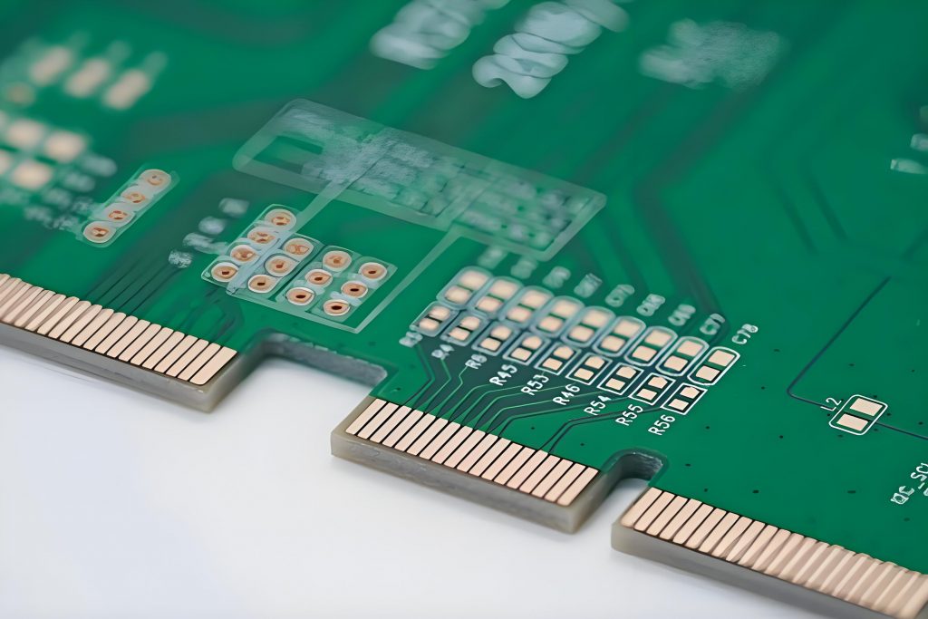
- Edge observation: Observe the edge of the PCB. If you can see multiple layers of copper foil lines or stacked boards, then this may be a multi-layer PCB. Each copper foil line represents an independent PCB layer.
- Solder mask color: Different layers of multi-layer PCBs are usually distinguished by solder mask layers of different colors. Check the surface of the PCB to see if there are areas of different colors, which may indicate differences between the layers.
- Printed markings: PCB manufacturers usually mark the number of layers on the PCB. Check if there are printed marks or labels on the PCB, which may show the number of layers of the PCB.
4. Other methods:
- Guide hole and blind hole light method: Determine the number of layers of the PCB by observing the guide holes and blind holes. The circuit connections of multi-layer PCBs all use guide hole technology. By observing the position and number of guide holes, the number of layers of the PCB can be preliminarily determined.
- Accumulation method: Determine the number of layers of the PCB by comparing the routing and component positions of some public board PCB boards. This method requires a certain amount of experience and accumulation.
What is the spacing for PCB layers?
The spacing of PCB layers is usually between 0.1mm and 0.3mm. Specifically, the recommended range of interlayer distance is 0.1-0.3mm to ensure sufficient spacing between layers to avoid signal interference and short circuits.
In addition, other spacing requirements need to be considered in PCB design:
- Spacing between conductors: The minimum line spacing must not be less than 4MIL, and the conventional spacing is 10MIL.
- Pad aperture and pad width: If mechanical drilling is used, the pad aperture must not be less than 0.2mm; if laser drilling is used, it must not be less than 4mil.
- Spacing between pads: Not less than 0.2mm.
- Spacing between copper and board edge: The spacing between live copper and PCB board edge is not less than 0.3mm. Large-area copper plating usually has an indentation distance from the board edge, which is generally set at 20mil.
These specifications and standards are designed to ensure the electrical performance, mechanical strength and manufacturing feasibility of PCBs.
How is a PCB board structured?
The basic structure of a PCB board includes four main layers: top layer, bottom layer, inner layer and pad layer.
The top layer is the topmost layer of the PCB board, which is full of electronic components such as resistors, capacitors and chips, and is responsible for connection and wiring to ensure the accurate transmission of current and signals. The bottom layer is located at the bottom of the PCB board, and is mainly responsible for the laying of ground wires and the connection of auxiliary signal lines, providing stable support.
The inner layer is located between the top layer and the bottom layer, and is composed of multiple layers of copper foil stacked to form a complex circuit network for signal transmission and power supply, reducing signal interference.
The pad layer covers the surface of the pad to prevent the solder from splashing into other areas during the welding process, protecting the welding quality and stability of the circuit board.
What are the small holes in printed circuit boards called?
There are many types of small holes on printed circuit boards, mainly including Via, Blind Via, Buried Via and Through Via.
1. Via: Vias are one of the most common types of holes in printed circuit boards, which are used for electrical connections between layers or for fixing and positioning devices. Vias can be divided into three types: blind holes, buried holes and through holes.
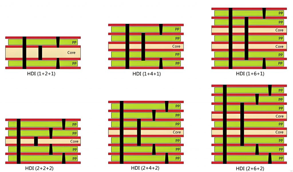
- Blind hole: a hole that connects the surface layer and the inner layer but does not penetrate the entire circuit board. It is suitable for high-density interconnection design and saves space.
- Buried hole: a hole located between the inner layers but does not extend to the outer layer. It is used for inner layer signal interconnection to reduce signal interference.
- Through hole: a hole that runs through the entire circuit board, used for internal interconnection or as a component positioning hole, easy to use and low cost.
2. Non-plated hole (NPTH): There is no copper on the inner wall of this hole. It is mainly used for positioning when assembling electronic components or connecting the joints of the panel.
3. Plated hole (PTH): including vias and pads. Vias are used for electrical connections between two layers, and pads are used to install plug-in electronic components.
4. Micro-Via: used for high-density PCB design to achieve more sophisticated wiring.
These different types of holes play different roles in printed circuit boards. Choosing the right hole type according to design requirements can improve the performance and reliability of the circuit board.
Each layer of the circuit board is indispensable. They work closely together to create a high-performance PCB circuit board. The substrate layer provides stable support, the signal layer transmits signals, the power layer provides power, the ground layer resists interference, the middle layer expands or isolates the circuit, and the silk screen layer assists in assembly.
Tags: layers to circuit board, PCB


