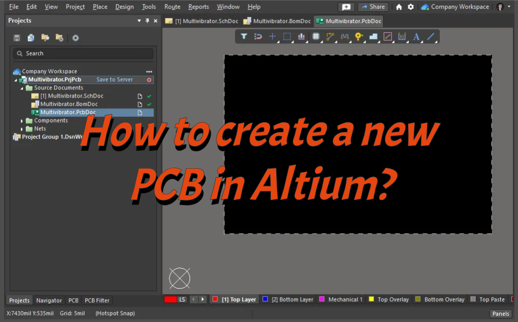
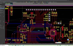
How to create a new PCB in Altium? To creating a new pcb in altium from schematic, finalize the schematic with all components and connections, then create a new PCB layout document. Arrange components in the workspace, define the board shape and layer stackup, and set design rules. Route the traces and verify the design using Altium’s Design Rule Check (DRC) to ensure it meets manufacturing and design standards.
How to create a new PCB in Altium?
Creating a new PCB in Altium mainly includes the following steps:
1. Create a new PCB file
- To create a new file: Open the Altium software, select the “File” menu, and then click the “New” option. In the pop-up submenu, select “PCB”, so that a new blank PCB file is created. You can also use the shortcut key “Ctrl + N”, and then select “PCB Document” in the pop-up “New Document” dialog box to create it.
2. Set PCB parameters
- Unit setting: Select “Document Option” in the “Design” menu. In the pop-up dialog box, you can select the unit of the PCB. Generally, there are two units to choose from: imperial (mil) and metric (mm).
- Grid setting: Also in the “Document Options” dialog box, switch to the “Grids” tab. You can set the Visible Grid and Snap Grid. The visible grid is used as a visual reference during the design process to help users align components and wiring.
- Define the board frame: You can use the “Line” tool or the “Keep – Out” tool in the “Place” menu to draw the border of the PCB. If you use the “Line” tool, you need to manually draw a closed polygon to represent the shape of the PCB; the area drawn with the “Keep – Out” tool indicates the range where wiring is prohibited, and can also be used as the boundary of the PCB.
- Precisely set the size: Select “Board Shape” in the “Design” menu, and then select “Redefine Board Shape”. At this time, the mouse cursor will become a cross shape. Use the mouse to click on the previously drawn board frame lines, and the software will automatically redefine the shape and size of the PCB based on these lines.
3. Add component library
- Open the component library panel: In the “Libraries” panel on the right, if it is not displayed, you can open it through the “Workspace Panels” option in the “View” menu, and then select “Libraries”.
- Add library files: In the component library panel, click the “Libraries” button, and in the pop-up “Available Libraries” dialog box, select the “Install” option. Then find the required component library file in the file browser (usually *.IntLib or *.SchLib and *.PcbLib files), select and click “Open” to add the component library to the software.
4. Place components
- Find components: After the component library is added, you can find the components that need to be placed on the PCB in the component library panel. You can quickly locate the component by entering the component name, model or package type in the search box.
- Place components: After finding the required component, double-click the component name or click the component name and select the “Place” option. The mouse cursor will change to the shape of the component. Move the mouse to the appropriate position in the PCB editing area and click the left mouse button to place the component. During the placement process, you can rotate the component by pressing the space bar to adjust the direction of the component.
5. Component layout
- Manual layout: After placing the component, you need to layout the component. When manually laying out, you can adjust the position of the component based on factors such as the electrical connection relationship between components, signal flow, and the mechanical structure of the PCB.
- Automatic layout (optional): Altium also provides an automatic layout function. Select the “Component Placement” option in the “Tools” menu, and then select “Auto Place”. However, the result of automatic layout may not be ideal, and manual adjustments are usually required based on the automatic layout to achieve the best layout effect.
6. Wiring
- Set wiring rules: Before wiring, you need to set wiring rules. Select the “Rules” option in the “Design” menu. In the pop-up “PCB Rules and Constraints Editor” dialog box, you can set various routing rules such as line width, routing spacing, and via size.
- Start routing: Select the “Interactive Routing” option in the “Route” menu, or use the shortcut key “Ctrl + W”, and the mouse cursor will become a cross shape. Click a component pin as the starting point for routing, and then move the mouse to the target pin. The software will automatically generate routing according to the set routing rules. During the routing process, you can switch the routing mode by pressing the “Shift + Space” key combination, such as 45° routing, 90° routing, etc.
7. Design Verification
- Electrical Rule Check (ERC): Select the “Design Rule Check” option in the “Tools” menu. In the pop-up “Design Rule Check” dialog box, set the items and parameters to be checked, and then click the “Run DRC” button. The software will check whether the PCB design complies with the previously set routing rules, such as whether there are short circuits, open circuits, insufficient spacing, etc., and generate a check report.
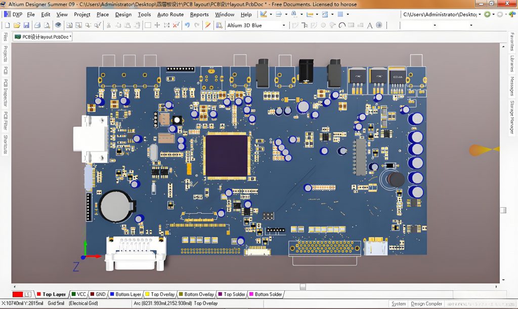
- 3D view check (optional): Altium also provides a 3D view function, which can help users check the PCB design more intuitively. Select the “Switch to 3D” option in the “View” menu, and the software will display the PCB design in 3D.
Through the above steps, you can create a new PCB in Altium. In the actual design process, you may need to repeatedly adjust and optimize each step according to the specific design requirements and complexity to obtain a high-quality PCB design.
What is the difference between a schematic and a PCB?
The main differences between a schematic and a PCB are in terms of definition, purpose, content, and form of expression.
1. Definition and purpose
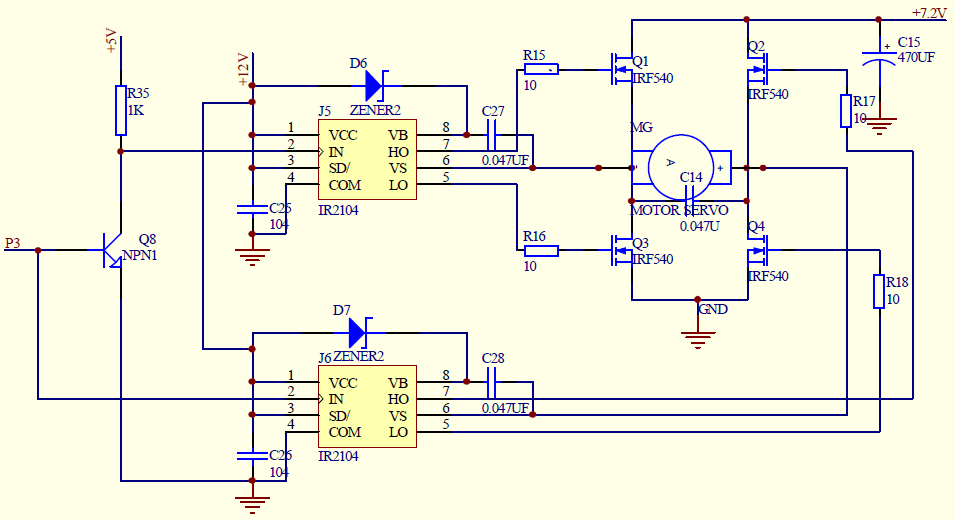
- Schematic: A schematic is also called a circuit diagram or electrical schematic. It uses graphic symbols to represent circuit components and their connections. The schematic mainly describes the working principle of an electronic device and does not involve a specific physical layout.
- PCB: A PCB diagram is a printed circuit board diagram, which is a mapping drawing of a circuit board, detailing the routing, component location, size, and connection method of the circuit board. PCB diagram is the direct basis for the actual production of circuit boards. It is mainly used to guide the manufacturing and assembly process of PCB boards to ensure that components are placed correctly and lines are connected accurately.
2. Content and form of expression
- Schematic diagram: The schematic diagram represents components and connection lines in a symbolic form, clearly showing the working principle and logical relationship of the circuit. It does not involve specific physical layout and size, so it is relatively flexible and easy to modify and optimize.
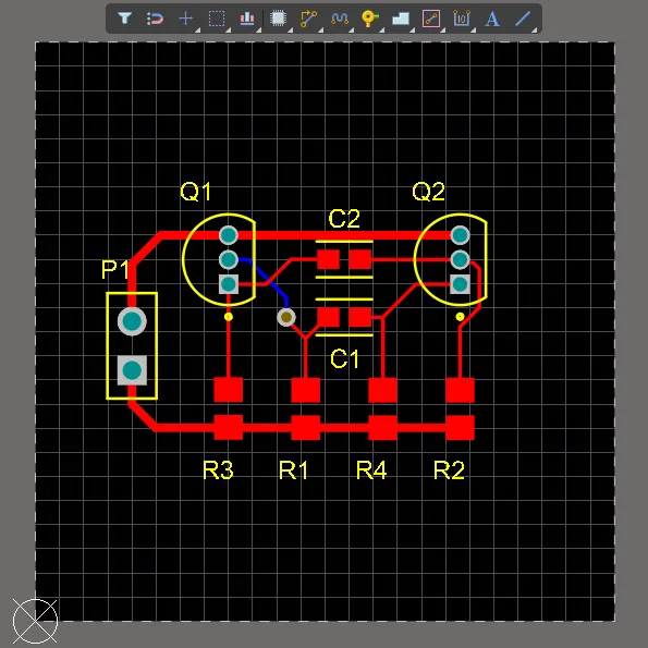
- PCB diagram: The PCB diagram shows the actual layout and electrical connection of components, including copper foil lines, pads and vias. PCB diagram is the basis of circuit board manufacturing, involving specific physical layout and connection methods. Once determined, the modification is more complicated.
How to make a PCB from schematic?
Making a PCB from a schematic can be divided into the following steps:
- Drawing a schematic diagram: Use circuit design software (such as Altium Designer, Eagle, etc.) to draw a circuit schematic diagram, including the connection relationship of each electronic component.
- Design PCB: According to the component layout and connection relationship in the schematic diagram, PCB layout design is performed in the PCB design software, including component placement, wiring, etc.
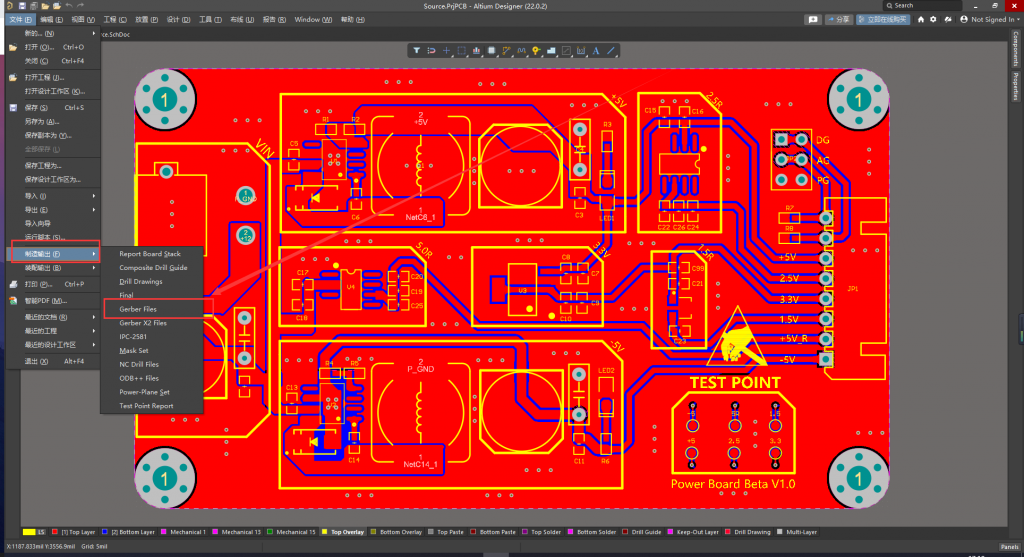
- Generate Gerber files: Export the designed PCB files as Gerber files, which is a standard PCB manufacturing file format that contains information about each layer of the PCB, such as copper foil layer, silk screen layer, solder mask layer, etc.
- Make PCB: Send the generated Gerber files to the PCB manufacturer or use PCB manufacturing equipment for production. The PCB manufacturer will make the actual PCB circuit board according to the Gerber file.
- Solder components: Solder the electronic components to the manufactured PCB circuit board to complete the circuit assembly.
- Test and debug: Test and debug the assembled circuit board to ensure that the circuit functions normally.
Can Altium open Gerber files?
Altium Designer can open Gerber files. The specific steps are as follows:
Open Altium Designer software, select “File” in the menu bar, then select “New”, and then click “Cam document” in its drop-down submenu to create a new CAM file.
In the newly created CAM file, select the “Import” sub-item of the “File” menu item, and then select “Gerber” to start importing Gerber files.
Select the Gerber file to be opened in the pop-up window, click “Open”, and then click the “OK” button in the pop-up “Import Gerber” window, and the Gerber file can be successfully opened.
How do I convert PCB to schematic in Altium?
To convert PCB to schematic in Altium, first open the PCB file and export the network table through the “Design” menu (select the appropriate format such as Protel format). Then create a new schematic file and import the previously exported network table through the “Design” menu. Then manually adjust the component layout to make it more reasonable, and finally check whether the connection relationship is correct and improve the schematic, add annotations and logos, etc.
How do you place components from schematic in Altium?
In Altium Designer, first make sure that the required component library has been added. If not, you can add it by opening it in the “Workspace Panels” under the “Libraries” panel menu. Click the “Libraries” button, select “Install) in the “Available Libraries” dialog box that pops up, and find the component library file (such as *.SchLib) and add it.
In the “Libraries” panel, enter keywords such as component name, model or package type in the search box to find the components to be placed. You can also expand the corresponding library folder in the library list and browse to find the components.
After finding the component, there are two ways to place it. One is to double-click the component name directly, and the mouse cursor will change to the shape of the component; the other is to click the component name and select the “Place” option.
Move the mouse to the schematic editing area and click the left mouse button to place the component in the appropriate position. During the placement process, you can press the space bar to rotate the component and adjust its direction. Repeat this operation and place all the required components one by one into the schematic according to the schematic design.
How to make a PCB board step by step?
- PCB manufacturing: After receiving the file, the PCB manufacturer manufactures it according to the file information. The manufacturing process includes multiple process steps such as inner layer pattern production, lamination, outer layer pattern production, drilling, electroplating, solder mask coating and silk screen characters.
- Component assembly: After the PCB is manufactured, the components are assembled by manual welding or automated equipment, and the electronic components are installed on the PCB board according to the requirements of the BOM and schematic diagram to complete the production of the PCB board.
- Functional test: Use test equipment to perform functional tests on the assembled PCB board to check whether the circuit can work normally and whether it meets the design requirements.
- Performance debugging: For some complex circuits, performance debugging may be required, such as adjusting component parameters, optimizing signal processing, etc., to improve the performance and stability of the circuit.
In short, throughout the design process, continuous adjustments and optimizations are required to ensure the performance, reliability and manufacturability of the PCB. At the same time, Altium Designer also provides many other functions and tools to help you better complete PCB design tasks.
Tags: creating a new pcb in altium from schematic, PCB, pcb design, PCBA, schematic diagram


