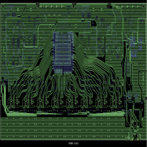
PCB designs are stored in various file types depending on the design software. The most common file type used is the Gerber file. It contains detailed information about each layer of the PCB, including traces, pads, and vias. These files guide the manufacturing process, ensuring every layer of the board is built precisely as intended.
Other formats like DXF, ODB++ and IPC-2581 are also used. They provide more comprehensive data, which can streamline the manufacturing process by reducing the need for multiple files.
What Is the Standard PCB File?
The Gerber file is recognized as the industry standard for PCB manufacturing. It serves as the blueprint that fabricators follow to build a PCB. Originally developed by Ucamco, the Gerber format has undergone multiple updates to enhance its functionality. Nowadays, the Gerber file is supported by virtually all PCB manufacturers and CAM (Computer-Aided Manufacturing) tools.
The standard gerber file format can be divided into RS-274 and RS-274X, Gerber X2 (gerber X2 is the latest version). The gerber file in RS-274 format is a separate file from aperture. aperture in RS-274X format is integrated into the gerber file. Generally speaking, a complete PCB Gerber file should include:
- Copper layers (top and bottom)
- Solder mask layers
- Silkscreen layers
- Drill files for holes
And below are some common terms used in a PCB file.
- .APR Aperture Data
- .GKO Keep Out Layer
- .GTO Top Overlay
- .GBO Bottom Overlay
- .GPT Top Pad Master
- .GPB Bottom Pad Master
- .GTS Top Solder Mask
- .GBS Bottom Solder Mask
- .GTL Top Layer
- .GBL Bottom Layer
- .GTP Top Solder Paste
- .GBP Bottom Solder Paste
- .G1 MidLayer1
- .G2 MidLayer2
- .G3 MidLayer3
- .G4 MidLayer4
- .GP1 Internal Plane1
- .GP2 Internal Plane2
- .GM1 Mechanical1
- .GM2 Mechanical2
- .GM3 Mechanical3
- .GM4 Mechanical4
- .GD1 Drill Drawing or NC
- .DRL Drill Data
- .TXT Drill Position
- .DRR Drill Tool size
- .LDP Drill Report
What Files Are Needed to Make a PCB?
To manufacture a PCB, several files are required, each serving a unique purpose. The essential files include:
- Schematic file
This is the start for PCB design. It shows the connection relation and component symbol of electronic circuit. For example, in a simple schematic diagram of the power supply circuit, it will clearly show the connection between the transformer, the rectifier diode, the filter capacitor and the voltage regulator chip. Through the schematic file, designers can clarify the function and signal flow of the entire circuit, providing the basis for subsequent PCB layout.
- PCB design file
This kind of file is generated on the basis of the schematic. It describes in detail the physical size of the PCB, the layer structure (such as 2-layer PCB, 4-layer PCB board, etc.), the component layout, the direction of the line and the holes. Take a four-layer PCB design file as an example, which will clearly indicate the distribution of signal layers, power layers, and ground plane layers. For component placement, it will be accurate to the coordinate position of each chip, resistor, capacitor and other components on the PCB board surface and their placement direction.
- Gerber file
These define the copper traces, pads, and component outlines for each layer.
- Drilling file
The drill file is used to indicate the drill location and dimensions on the PCB. In multilayer PCBS, the location and size of the holes are very critical. The drilling file tells the PCB manufacturing device exactly where the center coordinates of each hole are and the size of the aperture.
- Component coordinate file (.csv or.txt etc.)
The component coordinate File is also known as the “Pick and Place File”, which facilitates PCB assembly plants to perform component placement and plug-in operations.
This file contains the coordinate position of each component on the PCB board (X, Y coordinates), rotation Angle, component package type and other information. In an automated SMT production line, the mounter can accurately pick up the component from the strip and place it in the correct position on the PCB board based on the information in the component coordinate file.
- Bill of Materials (BOM)
A listing of all components’ details required for assembly, including part numbers, manufacturers, quantities and some marks.
What Is the Difference Between Gerber File and Board File?
A Gerber file is a manufacturing file. It describes the physical layout of the PCB layers, ready for fabrication. In contrast, a board file is a design file used within the PCB design software, such as Altium Designer, Eagle, or KiCad. Their key Differences are:
- Gerber File: Used for manufacturing; contains 2D layout data.
- Board File: Used for design; editable and contains schematic and layout information.
Manufacturers don’t use board files directly. They need Gerber files to fabricate the PCB.
What Is the Extension for a PCB File?
PCB files come with different extensions based on the software used to design them. Some common extensions include:
- .BRD: Used by Eagle and other design tools.
- .PCB: Common for Altium Designer and some older software.
- .GBR: The standard extension for Gerber files.
- .PcbDoc: Native to Altium Designer for saving PCB projects.
Each extension represents a different type of file, but they all contribute to the PCB design process.
How to Open a .PCB File?
How to open a .PCB file? Opening a .PCB file depends on the design software it was created with. Firstly, you should determine the software used to create the file. Common tools include Altium Designer, Eagle, and KiCad. Let’s take Altium as an example:
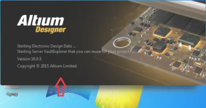
1. Install the Software: If you don’t have this software on your windows, please download and install the corresponding software firstly.
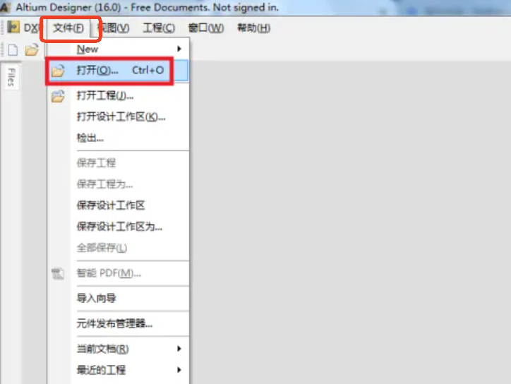
2. Open the File: Use the “Open” option within the software to load the .PCB file.
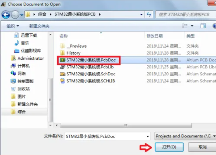
3. Choose the .PCB file what you want to open, and click “open”
4. Then you can check the PCB file by Altium Designer.
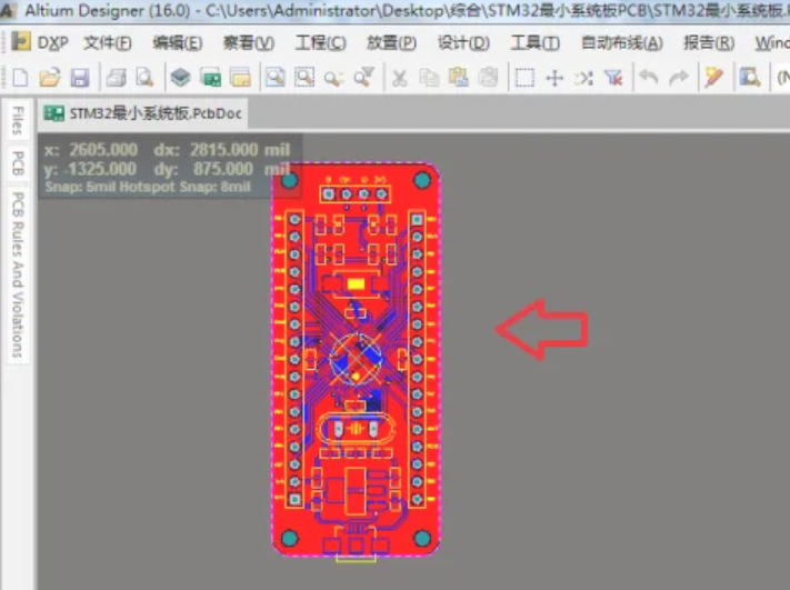
If you don’t have access to the original software, you can use a viewer like Gerbv or an online PCB viewer to inspect the file. However, these viewers may only provide a limited preview of the file and cannot edit it.
How Do I Convert a .PCB File to PDF?
Converting a .PCB file to a PDF is useful for sharing designs with clients or team members who don’t have design software. Here’s a simple way to do it with Altium Designer:
1. Open the .PCB File
Open a .PCB file; Click “File” → “Smart PDF(M)” in the toolbar successively, and the “Smart PDF Wizard” page pops up, as shown in FIG. 1 and FIG. 2 below;
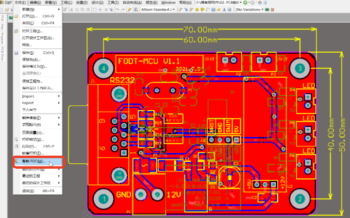
(FIG.1)
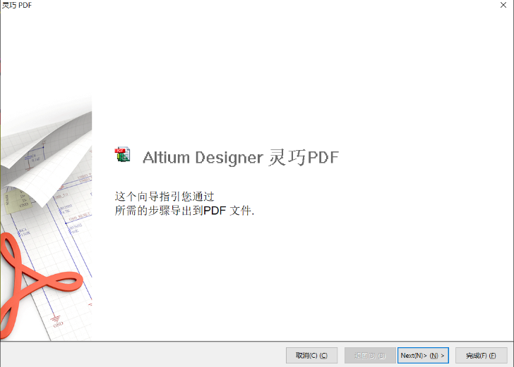
(FIG.2)
2. Export as PDF
In the smart PDF screen, click “Next” to enter the configuration selection screen for output PDF – including the following:
1). “Export Target File” + storage path and name of the output PDF file;
2). Whether to export the BOM table: If this parameter is selected, select the BOM table template. If it is not selected, click Next to go to the next step.
3). Set PDF printing parameters, according to the Settings of this page to determine the output of the entire PCB file or output a specific layer of files separately;
4). Set the “color” of PDF, there are “Color”, “monochrome”, “gray” options can be selected;
- “Color” option means the PDF file is output in accordance with the original color of each layer;
- “Monochrome” means the actual output of the file is all black;
- “Gray” means the actual output of the file is all gray display;
Below I choose the “Monochrome” option:
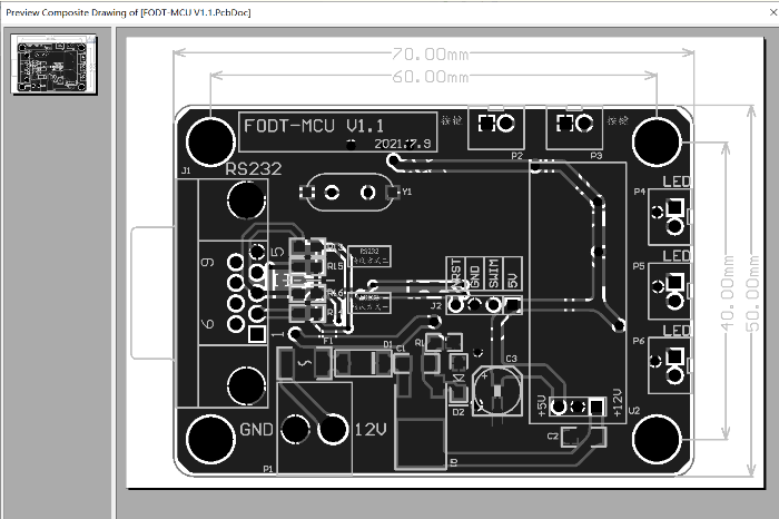
3. Enter “Print” and save the PDF: Choose a location and save the file.
Above are the end of this sharing, whether you’re dealing with Gerber files, board files, or converting formats, I hope this post is useful for you. If you have any other questions, welcome to e-mail with us at sales@bestpcbs.com, we are happy to help you.


