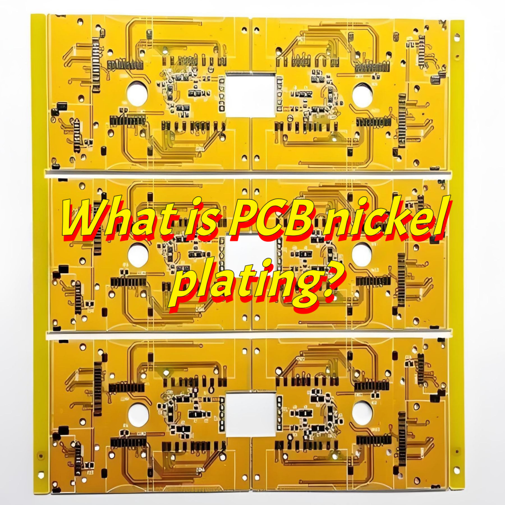
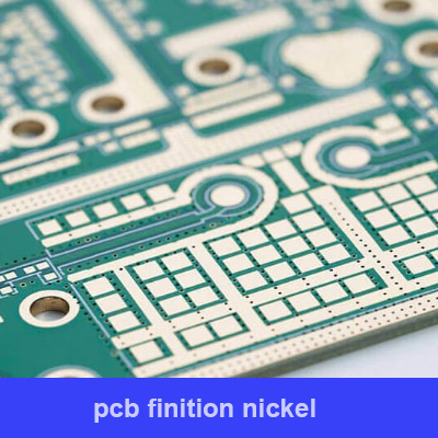
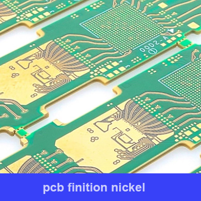
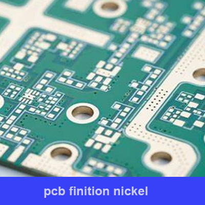
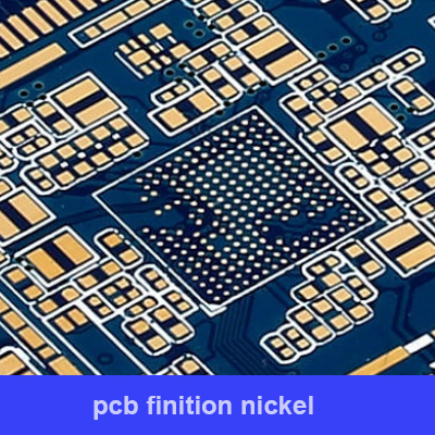
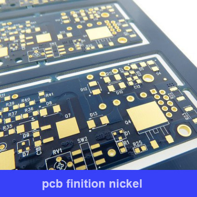
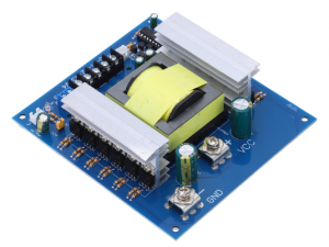
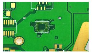
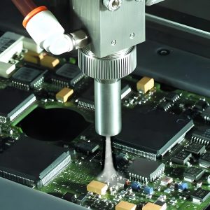
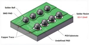
What is PCB nickel plating? PCB nickel plating refers to a layer of nickel covering on the surface of the circuit board. Its main function is to enhance the corrosion resistance, resistivity and solderability of the circuit board, while improving signal transmission performance and reliability. The nickel plating layer can protect the surface of the circuit board, prevent diffusion between metals, and improve the mechanical strength and durability of the circuit board.
PCB finition nickel or électrolytique soudabilité refers to the finishing process used on PCB to enhance solderability and protect exposed copper surfaces. Nickel is often applied as an underlayer, providing a robust, corrosion-resistant base for further finishes. Electrolytic finishes, such as electroplated gold or tin, are added on top to improve conductivity, durability, and ease of soldering. These finishes ensure reliable component attachment, minimize oxidation, and support the long-term performance of the PCB in various environments. The choice of nickel or an electrolytic finish depends on the specific application requirements, such as thermal resistance, electrical performance, and mechanical stability.
What is the function of PCB nickel plating?
The main functions of PCB nickel plating include improving wear resistance, preventing metal diffusion, enhancing mechanical strength, and adapting to the requirements of hot pressure welding and brazing.
Nickel plating on PCB (Printed Circuit Board) can significantly improve the wear resistance of switch contacts, contacts or plug gold. At the same time, the nickel layer acts as a barrier layer, which can effectively prevent the diffusion of copper and other metals, thereby protecting the circuit board. performance and lifespan.
In addition, the nickel layer can also improve the mechanical strength of the gold layer, making it more suitable as a substrate coating for precious and base metals.
- Corrosion resistance: The nickel plating layer can well protect the surface of the circuit board and enhance its corrosion resistance, allowing the circuit board to still operate stably in harsh environments.
- Resistivity: The resistivity of the circuit board can be increased by nickel plating, especially in high-frequency circuits, which improves the signal transmission quality of the circuit board.
- Solderability: Nickel plating makes the surface of the circuit board easier to handle, increasing its solderability.
- Signal transmission performance: The nickel plating layer has good electrical conductivity and can reduce signal transmission loss.
- Mechanical strength and durability: Nickel plating can increase the mechanical strength and durability of the circuit board and extend its service life.
How thick is PCB nickel plating?
The thickness of PCB nickel plating is usually around 2~2.5μm. The main function of the nickel plating layer is to serve as the bottom layer for gold or other precious metal plating, providing good bonding and protection. The thickness control of the nickel plating layer is very important for the appearance and quality of the product. Generally, a nickel layer thickness of about 5 μm is required to be sufficient.
PCB nickel plating thickness calculation formula
The calculation formula for PCB nickel plating layer thickness is: plating thickness (um) = current density (ASF) × plating time (min) × plating efficiency (%) × 0.01821.
Formula explanation
- Current Density (ASF): The number of amperes passing per unit area per square foot.
- Electroplating time (min): The time required for electroplating, in minutes.
- Electroplating efficiency (%): The actual utilization efficiency of current during the electroplating process, usually between 90% and 100%.
- 0.0182: This is a plating coefficient used to convert current density, plating time and plating efficiency into plating thickness.
Assuming that the current density is 10 ASF, the plating time is 30 minutes, and the plating efficiency is 95%, the thickness of the nickel plating layer is calculated as follows:
Current Density: 10 ASF
Plating time: 30 minutes
Plating efficiency: 95% (0.95)
Plating coefficient: 0.0182
Coating thickness = 10 × 30 × 0.95 × 0.0182 = 5.274 um
What are the differences between PCB nickel plating and tin spraying?
1. Process principle
- Nickel plating: Nickel plating is to electrochemically deposit a layer of metallic nickel on the surface of the circuit board. This process can enhance the electrical conductivity, corrosion resistance and welding performance of the circuit board.
- Spray tin: Spray tin uses thermal spray technology to spray a layer of tin alloy on the surface of the circuit board. The tin spray process can protect the circuit board from oxidation and corrosion while improving the reliability of welding.
2. Application effect
- Nickel plating effect: The surface of the circuit board after nickel plating has a uniform luster, and the nickel layer is closely combined with the base material, which can effectively resist the erosion of the external environment. In addition, the nickel layer also has good ductility and toughness, which is beneficial to subsequent processing and assembly.
- Tin spraying effect: The surface of the circuit board after tin spraying presents a dense tin alloy layer with good electrical conductivity and corrosion resistance. The tin spray process can also adjust the thickness and uniformity of the tin layer according to needs to meet the needs of different application scenarios.
3. Applicable scenarios
- Applicable scenarios for nickel plating: Nickel plating process is suitable for circuit boards with high requirements on conductivity, corrosion resistance and welding performance, such as communication equipment, automotive electronics and other fields. In addition, nickel plating is also commonly used for repair and reinforcement of circuit boards.
- Applicable scenarios for spray tin: The spray tin process is more suitable for circuit boards that require higher welding reliability and oxidation resistance, such as household appliances, industrial control and other fields. At the same time, the tin spray process is also suitable for decorative treatment on the surface of circuit boards.
The role of nickel sulfamate in pcb nickel plating
- 1. Improve electroplating efficiency: Nickel sulfamate can promote the electroplating reaction, significantly increase the electroplating speed, thereby shortening the electroplating time.
- 2. Improve coating quality: Nickel sulfamate can inhibit the crystallization of nickel in the electroplating solution, making it smaller and more uniform, thereby forming a denser and more uniform nickel coating.
- 3. Reduce internal stress: Nickel sulfamate helps reduce the internal stress of the coating, which is particularly important when plating complex-shaped objects to avoid cracking or peeling of the coating.
- 4. Control the pH value of the solution: Nickel sulfamate can maintain the stability of the pH value of the electroplating solution, which is crucial to ensuring the consistency of electroplating quality.
How to solder nickel-plated pins on PCB?
- Preparation before welding: Before welding, first apply flux on the pad and treat it with a soldering iron to prevent poor welding caused by poor tin plating or oxidation of the pad. For the chip, use tweezers to carefully place the PQFP chip on the PCB board, making sure the chip is placed in the correct orientation and the pins are aligned.
- Soldering the chip: Adjust the temperature of the soldering iron to above 300 degrees Celsius, dip a small amount of solder on the tip of the soldering iron, and use a tool to press down the aligned chip. Solder the two pins at diagonal locations to secure the chip. When soldering all pins, make sure the tip of the soldering iron is parallel to the soldering pins to prevent overlapping and overlapping soldering.
- Check and adjust: After soldering all pins, wet all pins with flux to clean the solder, suck off excess solder to eliminate shorts and overlaps. Use tweezers to check for mis-soldering.
Things to note when welding:
- Temperature control: Pay attention to temperature control when welding to avoid poor welding due to too high or too low temperature.
- Pin handling: During the soldering process, make sure the pins are moist to avoid weak soldering caused by improper pin handling.
Frequently asked questions and solutions:
- Pad Oxidation: If the pad is oxidized, it can lead to poor soldering. You can apply flux and treat the pads before soldering.
- Damaged pins: Be careful when using tweezers to avoid damaging the pins.
PCB nickel gold plating process
- Degreasing: First, the PCB is degreased to remove grease and dirt on the surface to ensure that the coating can be firmly adhered to the PCB surface.
- Water washing: After degreasing, wash with water to remove residual degreasing agent.
- Neutralization: Use a neutralizing agent to treat the PCB surface to adjust its pH value in preparation for subsequent steps.
- Water washing: After neutralization, wash again to ensure that the neutralizer residue is removed.
- Micro-etching: perform slight corrosion treatment on PCB to remove the oxide layer on the surface and increase the adhesion of the coating.
- Water washing: Wash with water after micro-etching to remove residual micro-etching agent.
- Pre-soak: Soak the PCB in a pre-soak solution to further prepare the surface.
- Palladium activation: Use palladium activation solution to treat the PCB surface to enhance the adhesion of the coating.
- Air blowing and agitation for water washing: Use air blowing and agitation for water washing to ensure that the surface is clean.
- Electroless nickel: A layer of electroless nickel is deposited on the surface of the PCB as the bottom layer.
- Hot water washing: After electroless nickel deposition, hot water washing is performed to remove residual electroless nickel solution.
- Electroless Gold: A layer of electroless gold is deposited on the electroless nickel layer to form the final gold plating layer.
- Recycling water washing: After electroless gold deposition, recycling water washing is performed to remove residual electroless gold solution.
- Post-processing water washing: Carry out final water washing to ensure the surface is clean.
- Drying: Finally, drying is performed to complete the entire nickel gold plating process.
PCB finition nickel or électrolytique effet champagne refers to a specific surface treatment that enhances the visual and functional qualities of printed circuit boards.
This finish involves the application of a nickel layer, often followed by an electrolytic coating such as gold, which creates a sparkling, champagne-like effect. The aesthetic appeal is complemented by functional advantages, including improved solderability, corrosion resistance, and enhanced conductivity.
The “effet champagne” is particularly desirable in high-end electronics or luxury applications, where both performance and appearance are critical. This finish ensures durability while delivering an elegant visual characteristic that sets the product apart.
PCB nickel plating layer adhesion test standard national standard
The national standard for PCB nickel plating layer adhesion testing is GB/T 9286-1998. This standard applies to coating adhesion testing, including nickel plating. Testing methods include peeling test, scratch test and impact test, etc. The specific test method chosen can be determined according to the characteristics and requirements of the test material.
Test method
- Cross-hatch test: Use a sharp blade to cut 10 × 10 small grids of 1 mm × 1 mm on the surface of the nickel plating layer. Each scratch line should be as deep as the bottom layer of the plating layer. Then use a soft brush to clean the debris in the test area, and stick a tape with an adhesion of 350 g/cm² to 400g/cm² (such as 3M No. 600 tape). After wiping hard, pull off the tape quickly in the vertical direction and observe the coating. Shedding condition.
- Peeling test: Peel off the nickel-plated sample and observe whether the coating peels off or deforms.
- Impact test: Conduct an impact test on the nickel plating layer to observe its impact resistance.
Judgment criteria
- 5B: The edge of the scribed line is smooth, and there is no coating peeling off at the edge and intersection of the scribed line.
- 4B: There is a small piece of coating peeling off at the intersection of the scribed lines, and the total peeling area is less than 5%.
- 3B: There are small pieces of coating peeling off at the edges and intersections of the scribed lines, and the total peeling area is between 5% and 15%.
- 2B: There are pieces of coating peeling off at the edges and intersections of the scribed lines, and the total peeling area is between 15% and 35%.
- 1B: There are pieces of coating peeling off at the edges and intersections of the scribed lines, and the total peeling area is between 35% and 65%.
- 0B: There are pieces of coating peeling off at the edges and intersections of the scribed lines, and the total peeling area is greater than 65%2.
PCB nickel plating process flow and solutions to common problems
- Surface treatment: Before nickel plating a circuit board, the surface of the circuit board needs to be properly treated to ensure that the surface finish and roughness meet the requirements.
- Electrolyte formula: The formula of electrolyte has a great influence on the quality of nickel plating on circuit boards. The formula and concentration need to be adjusted according to specific requirements.
- Coating thickness: Anti-corrosion performance is related to coating thickness and needs to be controlled according to actual needs.
- Nickel layer structure: The nickel layer obtained by nickel plating on the circuit board should be tight and strong, without defects such as cracks and pores.
- Subsequent processing: After nickel plating the circuit board, a series of subsequent processing is required, such as washing, polishing, cleaning, packaging and other operations.
PCB nickel plating is an important electronic manufacturing process, which can provide PCB with protection against copper oxidation, improve wear resistance, enhance corrosion resistance and improve welding performance. In the PCB nickel plating process, key points such as plating solution formula, process parameters, equipment and environment, and quality control need to be paid attention to to ensure the quality and consistency of nickel plating.
Tags: pcb finition nickel or electrolytique effet champagne, PCB finition nickel or électrolytique soudabilité, PCB nickel plating


