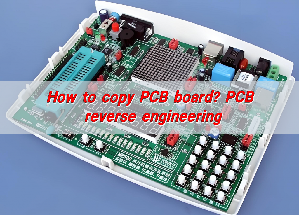
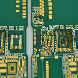
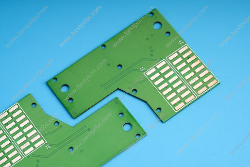
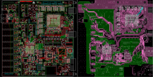
How to copy PCB board? PCB reverse engineering. First, get the PCB sample to be copied, then disassemble and record the component information on the sample to make a BOM table; then scan the sample to get its PCB layout image; then trace the routing and place the components according to the image to complete the drawing of the PCB diagram; finally, use the drawn PCB diagram to make a new PCB board, solder the corresponding components, and test and debug to ensure normal function.
What is copy PCB?
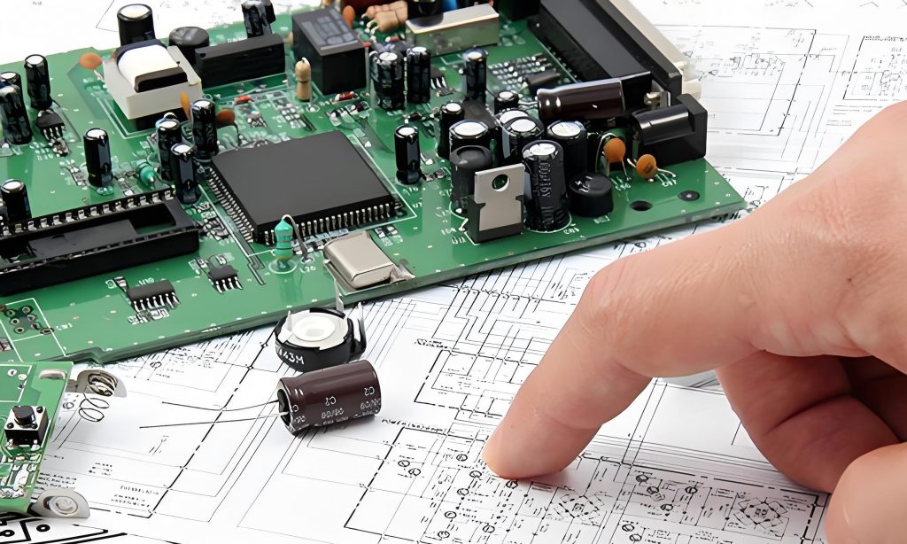
PCB copying, also known as circuit board cloning, refers to the reverse analysis of the circuit board through reverse research and development technology on the premise of existing electronic products and circuit boards, restoring the original product’s PCB files, bill of materials (BOM), schematic files and other technical files, and using these technical files to make PCB boards, solder components, test and debug, and finally complete the complete copy of the original circuit board sample.
How to copy PCB?
The process of copying PCB can be divided into the following points:
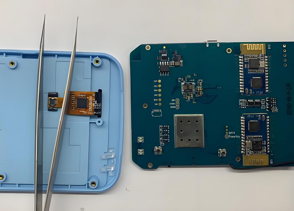
1. Get the PCB board to be copied and scan and back it up, remove the components and record the information to make a BOM table, and clean the residue on the surface of the PCB board.
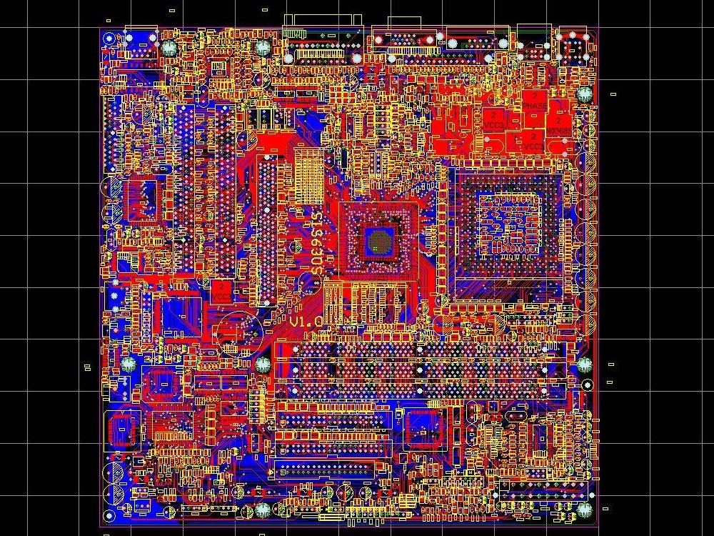
2. Scan the cleaned PCB board, import it into the copy board software, draw the routing and place the components according to the image, and export the PCB file.
3. Make the PCB file into a PCB board, test and debug after soldering the components, and ensure that the copied PCB board functions normally.
What are the steps to copy PCB?
The process of copying PCB can be divided into the following steps:
1. Preparation
- Get the PCB board: First, you need a PCB board, which can be provided by the customer or available on the market.
- Scan and back up: Scan and back up the PCB board for reference during the copying process.
2. Remove components
- Remove components: Use tools such as hot air guns to remove components on the PCB board, pay attention to temperature control, and avoid damaging components or PCB.
- Make a BOM table: Record the model, parameters, location and other information of the removed components, and make a bill of materials.
3. Clean the PCB board
- Remove residues: Clean the tin slag and other residues on the surface of the PCB board after the components are removed.
4. Copy board
- Scan the PCB board: Scan the cleaned PCB board again to obtain a clear image.
- Import the copy board software: Import the scanned image into the copy board software.
- Draw the routing and place components: In the copy board software, draw the routing of the PCB according to the scanned image and place the corresponding components.
- Export PCB file: Export the drawn PCB design to PCB file format.
5. Make and test
- Make PCB board: Make the exported PCB file into a PCB board.
- Weld components: Weld the purchased components to the made PCB board.
- Test and debug: Test and debug the welded PCB board to ensure its normal function.
Notes:
- Legal compliance: When copying PCB, you need to pay attention to relevant laws and regulations to avoid infringement of intellectual property rights.
- Precision control: During the scanning, drawing and production process, the precision must be strictly controlled to ensure that the copied PCB board is consistent with the original board
Does copy PCB comply with regulations?
Whether the copy PCB complies with regulations depends mainly on the purpose of the copy and whether the relevant intellectual property laws are complied with.
- Intellectual property respect: The intellectual property rights of the original design must be respected when copying the PCB.
- Legality of reverse engineering: In some cases, copying PCBs through reverse engineering is allowed, but the premise is that such behavior must be used for legitimate purposes.
In summary, whether the copying of PCBs is legal depends mainly on the purpose of the copying and whether the corresponding intellectual property license has been obtained. If it is for commercial purposes and without permission, it may violate relevant laws and regulations and face legal risks.
What are the benefits of copying PCB?
The benefits of copying PCBs mainly include the following aspects:
- Save time and cost: By copying PCBs, companies can avoid the high cost and time cost of designing from scratch. Especially in urgent and complex projects, it can significantly save time and manpower.
- Improve R&D efficiency: Copying PCBs can accelerate the product R&D process, shorten the product R&D cycle, and enable products to be brought to market faster.
- Optimize performance and function: Copying PCB is not just a simple copy. Through the analysis and research of technical data, product performance and function can be optimized, thereby enhancing the market competitiveness of products.
- Avoid intellectual property issues: By copying PCB, enterprises can avoid infringing on the intellectual property rights of others under the premise of legality.
What should I pay attention to when copying PCB?
The following points should be noted when copying PCB:
- Back up the original file: Before starting to copy, be sure to back up the original PCB file and GERBER file.
- Strict file operation: During the copying process, the PCB board must be remade strictly in accordance with the content in the GERBER file, and it cannot be modified at will.
- Check the file content: After exporting the GERBER file, you need to carefully check the file content to ensure the accuracy of the copy board content.
- Processing inner layer circuits: When processing the inner layer circuits, since there are only copper foil and inner circuits, the actual circuits cannot be seen, and the inner layer circuits need to be checked through the outer layer circuits.
- Copper plating: When plating copper, the copper foil and the inner circuit connection need to be disconnected to avoid connection with the outer circuit.
- Proofread with CAM software: After the design is completed, use CAM software for proofreading to ensure the accuracy of the copy board content.
- Record component information: Before copying, record the model, parameters and position of all components in detail, especially the direction of diodes and transistors and the direction of IC gaps.
- Disassemble and clean the PCB board: Remove all components, clean the PCB board, clean it with alcohol, dry it, and put it in the scanner.
- Image processing: Adjust the contrast and brightness to make the parts with and without copper film have a strong contrast. Remove noise, scratches, etc.
- Generate PCB file: Convert the processed image to PROTEL format file, import it in PROTEL and compare whether the PAD and VIA positions are accurately overlapped.
- Merge and verify: Import TOP.PCB and BOT.PCB in PROTEL and merge them into a complete PCB diagram. Use a laser printer to print the TOP layer and BOTTOM layer on a transparent film at a 1:1 ratio, and compare it with the original PCB to ensure that there is no error.
How does BEST Technology copy PCB?
As a professional PCB manufacturer, BEST Technology has the following process for copying PCB:
1. Submit sample photos
- Customer operation: Please take clear photos of the PCB samples, including the component layout and routing details on both sides, and then send the photos to our email: sales@bestpcbs.com
- Notes: Make sure the photos are clear enough to clearly show the component model, location and routing on the PCB board so that our engineers can conduct preliminary analysis and evaluation.
2. Preliminary quotation and communication
- Engineer evaluation: After receiving the sample photos, our engineers will give a rough copy price based on factors such as the complexity of the PCB in the photos, the number and type of components, etc.
- Program and IC information: If the PCB contains a program IC, you need to inform us or provide a clear photo of the IC so that we can evaluate the difficulty and cost of program cracking and give a more accurate quotation.
3. Confirm the price and send samples
- Price confirmation: After receiving our preliminary quotation, if you have any questions or need to adjust, you can communicate with us further until both parties reach an agreement on the price.
- Sample delivery: After the price is determined, you need to send us PCB samples, preferably 2 samples, so that we can conduct more detailed analysis and cloning. After receiving the samples, we will provide you with an accurate quotation based on the actual sample situation.
4. Payment and production start
- Payment process: After you confirm that the final quotation is correct, you will complete the payment according to our payment method.
- Production start: After receiving the customer’s payment, we will officially start the PCB cloning work, including sample analysis, component disassembly, PCB drawing and other steps.
5. Provide design files and manufacture circuit boards
- Design file delivery: After completing the copy board work, we will send you the complete Gerber file, schematic diagram and BOM (Bill of Materials) for your review and confirmation.
- Circuit board manufacturing: After confirming that the design files are correct, we will start to manufacture circuit boards for you based on these files to ensure that the quality and performance of the circuit boards meet your requirements.
In summary, every step of the PCB copy process is meticulous to ensure that the copy board accurately restores the original board function. At the same time, it is very necessary to find a qualified PCB manufacturer. BEST Technology has rich experience in PCB manufacturing. If you have PCB copy needs, please feel free to contact us at sales@bestpcbs.com.
Tags: copy PCB, PCB reverse engineering


