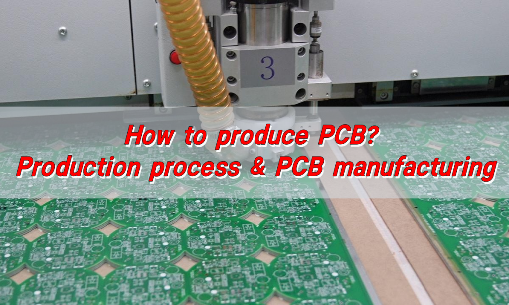
How to produce PCB? To produce a PCB, you must first design the schematic and PCB layout, then make a blank, then drill holes and copper plate it, and finally perform etching, surface treatment and other processes to etch the copper foil into a circuit pattern to complete the PCB production.
How to Manufacture PCBs?
- 1. Designing the PCB Layout
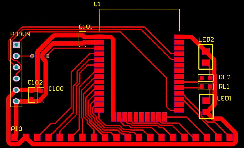
The first step is designing the circuit using specialized software. Tools like Eagle, Altium Designer, or KiCad allow engineers to create detailed blueprints, specifying copper traces, pads, and components. Precision at this stage ensures optimal functionality.
- 2. Printing the Design
Once the layout is finalized, it is transferred onto a physical board. The process involves printing the design onto a transparent film, which acts as a stencil for the subsequent steps.
- 3. Preparing the Base Material
The base material, typically fiberglass or FR4, is cleaned and prepped. This ensures proper adhesion of the copper layer.
- 4. Laminating the Copper Layer
A thin layer of copper is laminated onto the base material. This copper layer forms the conductive pathways of the PCB.
- 5. Applying the Photoresist
Photoresist, a light-sensitive material, is applied to the copper layer. UV light is then used to harden the areas matching the PCB design.
- 6. Etching the Copper
Unwanted copper is removed through chemical etching, leaving behind only the necessary conductive traces. This step defines the electrical pathways.
- 7. Drilling the Holes
Precise holes are drilled to accommodate components and vias. Modern laser drilling methods ensure high accuracy, especially for multilayer PCBs.
- 8. Plating and Surface Finishing
The drilled holes and traces are plated with additional copper for conductivity. Surface finishes, like HASL or ENIG, are applied to prevent oxidation.
- 9. Solder Mask Application
A solder mask is applied to protect the copper traces from environmental damage. This layer also prevents accidental solder bridging during assembly.
- 10. Silkscreen Printing
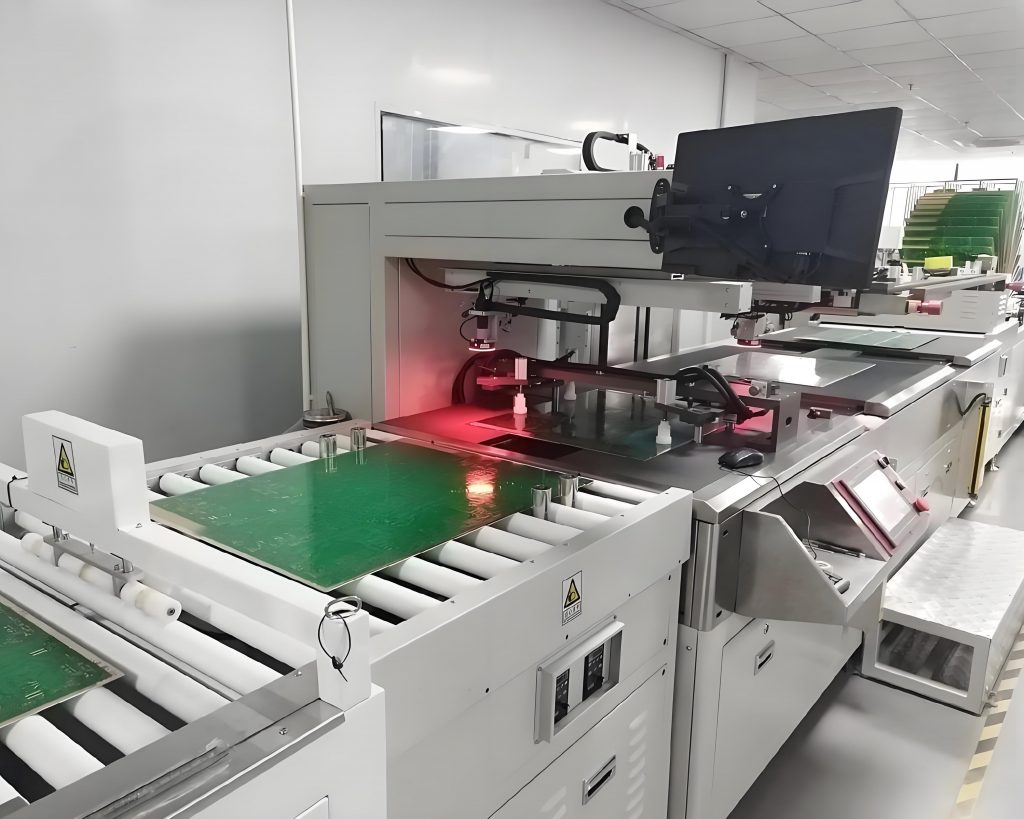
Silkscreen printing adds labels, logos, and component identifiers, aiding assembly and maintenance.
- 11. Final Inspection and Testing
Each PCB undergoes rigorous testing, including Automated Optical Inspection (AOI) and functional tests, to ensure quality and reliability.
How Is a PCB Created?
The creation of a PCB on software begins with designing the layout using advanced tools like Altium Designer or KiCad.
Engineers outline copper traces, pads, and components to create a functional design. Once finalized, this digital blueprint guides the subsequent physical manufacturing process.
The collaboration between engineers and PCB producers ensures accuracy and a seamless transition from design to production.
Are PCBs Expensive to Manufacture?
The cost of producing PCBs depends on various factors:
- Complexity: Multilayer boards cost more due to additional steps.
- Material: High-grade materials like ceramic or polyimide are pricier.
- Volume: Bulk production reduces unit costs.
- Customization: Specialized designs, such as rigid-flex PCBs, increase costs.
However, advances in technology and competition among PCB producers, especially in Asia and Europe, have made PCB production more affordable.
What Is the Cheapest Way to Make a PCB?
For cost-effective PCB production, consider these tips:
- Use Standard Materials: FR4 is a budget-friendly and reliable choice.
- Simplify the Design: Minimize layers and avoid intricate features.
- Order in Bulk: Larger quantities lower per-unit costs.
- Work with Trusted Producers: Established PCB producers often offer better prices due to streamlined processes.
How Long Does It Take to Make a PCB?
Lead times vary based on complexity and order size:
- Prototype PCBs: 3-5 days on average.
- Mass Production: 1-3 weeks, depending on volume and customizations.
Fast-turn options are available but come at a premium. Choosing established PCB producers can also shorten lead times.
What Is the Failure Rate of Producing PCBs?
Modern manufacturing techniques ensure low failure rates, often below 1%. However, challenges like poor material quality, design errors, or environmental factors can increase defects. Partnering with experienced PCB producers minimizes these risks.
What Are the Common Problems When Producing PCBs?
Some frequent issues include:
- Incomplete Etching: Residual copper can cause shorts.
- Misaligned Layers: Multilayer boards require precise alignment.
- Insufficient Drilling Accuracy: Impacts component placement and conductivity.
- Soldering Issues: Cold joints or bridging can occur during assembly.
- Design Errors: Incorrect layouts result in non-functional boards.
Quality control measures and working with top PCB producers can address these challenges effectively.
Where Are PCBs Most Commonly Found?
PCBs are integral to various industries:
- Consumer Electronics: Smartphones, laptops, and TVs.
- Automotive: Engine control units and infotainment systems.
- Healthcare: Medical devices like pacemakers and monitors.
- Aerospace: Navigation systems and avionics.
- Industrial Equipment: Machinery control systems and sensors.
Their versatility makes PCBs indispensable in modern technology.
Conclusion:
Producing PCBs involves a blend of engineering precision and advanced manufacturing techniques. Partnering with reputable PCB producers ensures quality, reliability, and efficiency in your projects. BEST Technology’s PCB production capabilities have been tested for 18 years and we have accumulated rich experience in the production and manufacturing of various types of PCBs. If you have any needs for PCB production, please feel free to contact us at sales@bestpcbs.com
Tags: pcb manufacturing, pcb producer, produce PCB, top pcb producers


