
What is Direct Thermal Path MCPCB?
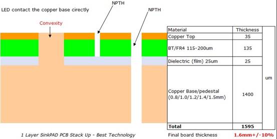
A Direct Thermal Path MCPCB (DTP MCPCB) also called sink Pad MCPCB, or thermoelectric separation MCPCB. It is a specialized type of metal-core PCB that design with a thermal convexity Pad to create a direct thermal path. It made of copper core/pedestal, so that the thermal Pad of LED chips can touch the convexity area of metal core directly, ensure a better heat dissipation.
The core of these boards is typically made of copper for ultra-high conductivity. The magic happens in the convexity Pad —a thin, thermally conductive that bonds the circuit layer to the metal base directly. See the stack up of a direct thermal path PCB as below for make sense:
Why Does Direct Thermal Path PCB Matter?
Heat is the enemy of electronics. When components overheat, performance drops, lifespans shorten, and failure risks rise. For example, an LED’s brightness can fade by 30% if its temperature rises just 20°C above optimal levels. Direct Thermal Path MCPCBs solve this by:
- Cutting thermal resistance: Heat escapes 8–10x faster than in standard boards.
- Preventing hotspots: Even temperature distribution avoids component burnout.
- Improving reliability: Cooler parts = 50% fewer breakdowns in harsh environments.
For industries where reliability is non-negotiable—like aerospace or medical devices—this tech is a game-changer. A drone’s flight controller using DTP MCPCBs, for instance, can handle prolonged use without throttling performance.
Benefits of Direct Thermal Path MCPCB
- Superior Heat Management: Direct contact with the metal core allows faster heat transfer, 8–10x faster than standard FR4 PCBs.
- Higher Component Reliability: Stable temperatures reduce stress on electronic parts.
- Compact Designs: No bulky heatsinks needed—ideal for slim devices like VR headsets.
- Longer Lifespan: Heat-sensitive components last longer due to better thermal management.
- Cost-Effective: Fewer cooling parts mounted, reducing 15-20% assembly costs.
- Versatility: Works in extreme temps (-50°C to 300°C).
- Increased Energy Efficiency: Lower thermal resistance enhances overall power efficiency.
- Consistent Performance – Devices run more reliably under high-power conditions.
Direct Thermal Path MCPCB Key Components
The materials used in DTP MCPCBs play a significant role in performance. Common options include:
1. Metal Core (Base Layer)
The metal core provides structural integrity and acts as the primary heat dissipator. Options include:
- Copper – Mostly used. Superior thermal performance (up to 400 W/m·K) but heavier and more expensive.
- Aluminum – Lightweight, but it is rarely made, because normal aluminum PCB can meet most of heat dissipation needs.
2. Circuit Layer (Copper Foil)
1oz to 6oz copper thickness depending on the application. Thicker copper enhances current-carrying capacity and heat dissipation.
3. Dielectric Layer (Optional in Some Designs)
- In regular MCPCBs, this layer insulates the circuit from the metal core.
- In DTP MCPCBs, selected areas have no dielectric layer, ensuring direct heat transfer.
4. Solder Mask & Silkscreen & Surface Finish
- Solder Mask – Protects the copper circuit from oxidation and damage.
- Silkscreen – Printing labels, company logo, trace names etc for identifying and smooth PCB assembly process.
- Surface Finishes – Options like ENIG, OSP, or HASL prevent corrosion and enhance solderability.
Types of Direct Thermal Path MCPCB
- Single-Layer DTP:
Basic design with one conductive layer.
Ideal for simple LED lighting (e.g., household bulbs).
Cost-effective for high-volume production.
- Double-Layer DTP:
Extra layer for complex circuits.
Used in automotive controls (e.g., EV battery monitors).
Supports moderate power loads (50–100W).
- Multi-Layer DTP:
Advanced setups with 4+ layers for high-density electronics.
Common in servers, 5G infrastructure, and industrial robots.
Handles 200W+ components with ease.
For more information of each type and direct thermal path MCPCB stack up, click into our official website:
DTP MCPCB vs. Regular MCPCB
The thermal conductivity of the thermoelectric separation MCPCB is as high as 380W/m.K, which is much higher than the 1-2W/m.K of the regular metal core PCB. The thermoelectric separation structure makes the LED chip directly touch with copper substrate, reducing the thermal resistance, thus improving the heat dissipation effect. In addition to this, the fabrication process of DTP MCPCB is more complex, manufacturers need to purchase copper base and insulation layer, then processing and laminating separately. Here are some other differences between the two:
| Feature | DTP MCPCB | Regular MCPCB |
| Thermal Resistance | Lower due to direct heat path | Higher due to dielectric layer |
| Heat Dissipation | Faster and more efficient | Slower, limited by dielectric layer |
| Weight | Slightly heavier due to copper core | Lighter in some cases (when used aluminum as core) |
| Thermal Path | Direct (no gaps) | Insulated (slower transfer) |
| Applications | EVs, industrial lasers | Consumer electronics, low-power |
Applications of Direct Thermal Path MCPCB
DTP MCPCBs are widely used in industries requiring high-performance thermal solutions:
LED Lighting – Enhances efficiency and longevity in high-brightness LED modules.
Power Electronics – Used in inverters, power supplies, and energy storage systems.
Telecommunication – Improves stability in high-frequency and RF applications.
Medical Devices – Ensures reliability in imaging systems and diagnostic tools.
Automotive Industry – Supports high-power applications like EV battery management.
Aerospace & Defense – Used in radar systems and avionics for thermal stability.
Manufacturing Process of Direct Thermal Path MCPCB
1. Preparation of Manufacturing Files
The first step is preparing the manufacturing files. This involves separating the copper core and circuit traces from a single Gerber layer into two distinct layers. The trace layer contains only the circuit traces without the central heatsink pad of the LED, while the copper core layer consists solely of the heatsink pad. This separation ensures precise processing in later stages.
2. Production of the Trace Layer and Copper Core Layer
Both layers are produced separately.
- Trace Layer Production
The trace layer follows a standard PCB manufacturing process, using materials like FR4 or BT (Bismaleimide-Triazine), with BT being the preferred choice due to its thermal properties.
- Copper Core Layer Processing
Processing the copper core is more complex.
a) The copper core thickness typically ranges from 0.8mm to 2.0mm and comes with protective blue film on both sides. The film is removed before etching to expose the copper surface.
b) After the raw material is cut, the copper core undergoes grinding to remove impurities, ensuring a clean surface for the next steps.
c) A blue film layer is applied over the entire copper core. After the developing and etching process, only selected areas of the blue film remain, marking the locations of the heatsink pad.
3. Lamination of the Trace Layer and Copper Core Layer
Once both layers are prepared, they are laminated together.
- Glue is applied to the bottom side of the trace layer for bonding.
- CNC milling/routing is performed to remove the cutout areas where the raised heatsink pad will be placed.
- After peeling off the white release paper, the trace layer is aligned and placed onto the copper core, forming the SinkPAD structure that enhances thermal performance.
4. Solder Mask Application
After hot lamination, the boards are cleaned before applying the solder mask.
- A stencil is used to align the board before printing solder mask ink.
- The solder mask color is applied using either a manual process for small batches or an automatic printer for mass production. Common colors include white, black, green, blue, yellow, and red.
- The boards are left to stand for one hour before being baked in an oven.
- The solder mask is then developed using UV light exposure and etched, leaving only the required solder mask areas.
5. Silkscreen Printing
Silkscreen markings are printed using a silk-screening process without requiring additional development or etching. This step ensures component labels and markings are clearly visible.
6. Surface Finishing
A suitable surface treatment is applied to the exposed copper areas to improve solderability and prevent oxidation.
- Common finishes include OSP (Organic Solderability Preservative) and ENIG (Electroless Nickel Immersion Gold).
- HAL (Hot Air Leveling) is not used for SinkPAD boards due to process limitations.
- Special surface finishes can be applied based on customer requirements.
7. Final Inspection and Shipment
Each board undergoes a strict electrical test (E-testing) and final quality control (FQC) to verify circuit integrity and manufacturing accuracy. Once approved, the boards are carefully packed and shipped according to customer specifications.
Throughout the entire process, every step is closely monitored to ensure high-quality solder masks, precise silkscreen printing, and flawless surface finishing, meeting all design and performance expectations.
Why Choose Best Technology?
With over 18 years of experience, Best Technology is a trusted name in PCB manufacturing. Our DTP MCPCBs deliver superior thermal management, longer lifespan, and excellent performance. Whether you need high-power LED PCBs, automotive PCBs, or industrial thermal solutions, we provide tailored solutions to meet your needs.
Our Direct Thermal Path MCPCB Manufacturing Capability
Best Technology specializes in custom DTP MCPCBs with the following capabilities:
Base material: Copper core: 0.8mm, 1.0mm, 1.2mm, 1.4mm, 1.5mm
Thermal Conductivity: 400 W/m.K.
Board Thickness: 1.0 mm~2.0mm(0.04″~0.08″)
Copper thickness: 0.5 OZ, 1.0 OZ, 2OZ, (specially 3-10 OZ)
Outline: Routing, punching, V-Cut
Soldermask: White/Black/Blue/Green/Red Oil
Legend/Silkscreen Color: Black/White/Yellow
Surface finishing: Immersion Gold, ENEPIG, Immersion Tin, OSP
Max Panel size: 600*500mm(23.62″*19.68″)
Packing: Vacuum/Plastic bag
Samples L/T: 1.5~2.5 weeks
MP L/T: 2.5~3.5 weeks
For premium Direct Thermal Path MCPCBs, contact Best Technology today!
You may also like


Tags: Direct Thermal Path MCPCB, thermoelectric separation MCPCB