
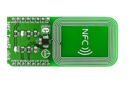
What Is NFC Antenna PCB?
An NFC antenna PCB is a printed circuit board with an integrated antenna that facilitates wireless communication between NFC-enabled devices. The full name of NFC is near-field communication. The antenna consists of copper traces in a loop configuration, which generate an electromagnetic field at 13.56 MHz—the standard NFC operating frequency.
These antennas are widely used in smartphones, payment terminals, public transport systems, industrial automation, and medical applications. The size, shape, and material of the NFC antenna PCB significantly impact performance, affecting signal strength, data transfer efficiency, and overall range.
What Is the Frequency Range of NFC Antenna PCB?
NFC technology operates within the high-frequency (HF) band at 13.56 MHz, which is globally standardized and regulated by ISO/IEC 14443, ISO/IEC 15693, and NFC Forum standards. But during the manufacturing, the frequency of NFC antenna PCB will be affected by some factors, we need to understand and avoid these factors:
- Antenna Size & Design: Larger antennas can enhance the range but may require more PCB space.
- Material Quality: Low-loss substrates help maintain signal integrity.
- Environmental Interference: Nearby metal objects can weaken NFC signals.
- Power Supply & Circuit Tuning: Proper tuning ensures stable operation at 13.56 MHz.
Since NFC operates at a fixed frequency, design and tuning adjustments are essential for achieving optimal performance.
What Does NFC Antenna PCB Do?
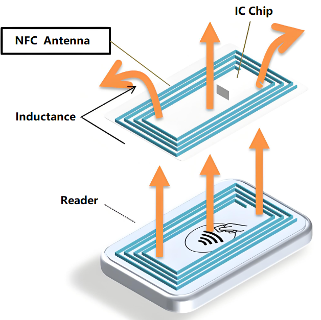
The primary function of an NFC antenna PCB is to enable short-range wireless communication between devices. It allows for fast, secure, and contactless data transfer, making it indispensable for applications like mobile payments, authentication, and access control. Let’s see how it works:
- Signal Transmission: An NFC reader generates a magnetic field at 13.56 MHz, which activates passive NFC tags or interacts with other NFC-enabled devices.
- Magnetic Coupling: When a compatible device enters the field, energy is transferred between the reader and the target device through inductive coupling.
- Data Exchange: Once connected, the devices can exchange information, process transactions, or verify identity.
What Is the Difference Between NFC Antenna Size and Range?
In general, the larger your antenna size, the longer the reading distance. Similarly a smaller antenna will give you a shorter read range. However, bigger isn’t always better, as factors like impedance matching and power output also play a role. It’s best to attempt to match the tag and the reader antenna geometries for maximum efficiency.
| Antenna Size | Range | Considerations |
| Small (10–20 mm) | Short (1–2 cm) | Used in compact devices like smartphones & wearables |
| Medium (20–50 mm) | Moderate (3–5 cm) | Common in payment terminals, industrial scanners |
| Large (50–100 mm) | Longer (5–10 cm) | Found in access control & long-range NFC readers |
A well-balanced antenna design ensures optimal performance while minimizing power loss. At Best Technology, we have experienced engineering team can offer you a best NFC antenna PCB solution, if you have some questions or challenges during design phrase, be sure to contact us at sales@bestpcbs.com.
How Long Is NFC Antenna Cable?
A typical NFC antenna cable is usually around 75mm long, although this can vary depending on the specific antenna design and manufacturer; many commercially available NFC antennas come with a cable length explicitly stated as 75mm. Longer cables may experience higher resistance and energy dissipation, requiring careful impedance matching for efficient signal transfer.
- Short Cables (50–100 mm): Found in smartphones, smart cards, and wearable devices to minimize resistance.
- Medium-Length Cables (100–300 mm): Used in POS terminals, smart locks, and kiosks for flexibility.
- Long Cables (300+ mm): Used in industrial applications, often requiring shielding to prevent signal loss.
Where Is the NFC Antenna on My Phone?
Nowadays, most smartphones have the NFC antenna integrated into the mainboard, it is always located on the back panel, usually near the top or center. In this way, we can ensure the optimal contactless transactions with payment terminals and other NFC devices. If you want to locate the NFC antenna on your phone, try to use below methods:
1. Check the phone’s manual for NFC placement details, it always show where the NFC antenna and how to use it.
2. Look for the NFC logo on the back of the phone.
3. Use an NFC-enabled card—move it around the back of the phone until it responds.
What Is the Impedance of NFC Antenna PCB?
The impedance of an NFC antenna PCB typically ranges between 50ohm and 200ohm, with 50ohm being the most common standard. Since NFC operates at 13.56 MHz, impedance matching ensures that the maximum amount of power is transmitted between the antenna and the NFC controller. Poor impedance matching can lead to signal reflection, power loss, and reduced communication range. Factors affecting NFC antenna PCB impedance including:
- Antenna size and shape: The number of turns and the loop configuration affect inductance and resistance.
- Substrate material: Different PCB materials have varying dielectric constants, impacting impedance.
- Trace width and spacing: Wider traces lower resistance, while spacing affects mutual inductance.
- Environmental factors: Nearby metals and circuit components can alter the effective impedance.
How Do I Check My Antenna Impedance?
To measure NFC antenna PCB impedance, use specialized RF measurement tools such as a Vector Network Analyzer (VNA) or an impedance bridge. Let’s take VNA for example, here is a step-by-step process to measure antenna impedance:
1. Connect the Antenna to a VNA: Attach the antenna’s feedline to the VNA using a coaxial cable with known impedance.
2. Perform S11 Parameter Measurement: The S11 reflection coefficient indicates how much energy is reflected back from the antenna. A lower value (closer to 0 dB) means better impedance matching.
3. Analyze the Smith Chart: The Smith chart helps visualize impedance variations and determine required adjustments.
4. Use a Matching Circuit: If impedance is off, introduce capacitors or inductors to fine-tune the circuit.
5. Verify with Load Testing: Apply an NFC reader and test real-world performance to confirm effective impedance matching.
Alternative Methods:
- Impedance Bridge: This measures resistance and reactance separately, providing a simple yet effective impedance estimation.
- Oscilloscope & Signal Generator: While not as precise as a VNA, this setup can provide insights into impedance variations under different frequencies.
NFC PCB Antenna Design Guide
Designing an NFC PCB antenna requires careful consideration of parameters like inductance, impedance matching, material selection, and trace layout. The goal is to optimize signal strength, communication range, and energy efficiency at the 13.56 MHz operating frequency. A well-designed antenna ensures stable and reliable NFC performance in various applications, from contactless payments to IoT connectivity.
1. Selecting the Right Substrate Material
The PCB material plays a crucial role in NFC antenna performance. Since NFC operates at low frequencies, FR4 is a common choice due to its cost-effectiveness and availability. However, its dielectric constant (Dk) varies, which can affect impedance, higher Dk values lead to higher signal attenuation. For better performance, materials with low loss tangents, such as Rogers laminates, can help maintain signal integrity.
2. Determining the Antenna Shape and Size
The most common NFC antenna shapes are listing as below, you can choose one according to your specific end-applications.
- Rectangular: Common for mobile and industrial applications.
- Circular: Used in smart cards and compact devices.
- Custom: Designed for unique applications where space constraints exist.
Key considerations for antenna size:
- Larger antennas offer better coupling and longer range.
- Smaller antennas are suitable for compact devices but require careful tuning.
Number of turns in the coil affects inductance—more turns increase inductance but may reduce efficiency.
3. Calculating Inductance and Matching Circuit
For optimal NFC performance, the antenna must have the right inductance to match the NFC controller’s impedance. The standard inductance for NFC antennas ranges from 1.5 µH to 3.5 µH, depending on the application. The inductance (L) of a loop antenna can be estimated using below formula:

Where:
- μ0 is the permeability of free space
- N is the number of turns
- A is the loop area
- l is the total length of the conductor
If the inductance is too high or too low, adjustments can be made by:
- Changing the number of turns in the coil.
- Modifying the trace width and spacing.
- Adding a matching network with capacitors to fine-tune resonance.
4. Designing the Trace Layout
The layout of the antenna traces impacts signal transmission and efficiency. Best practices for NFC PCB antenna traces:
✔ Use smooth curves instead of sharp angles to prevent signal distortion.
✔ Keep trace width uniform to maintain consistent inductance.
✔ Ensure even spacing between turns to minimize interference.
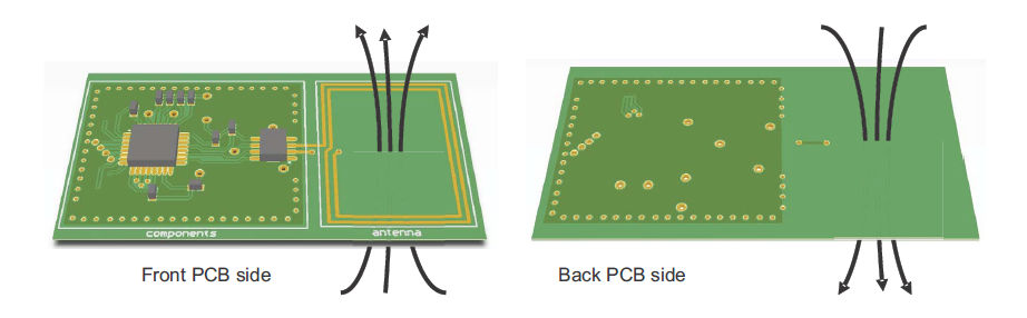
✔ Avoid placing components near the antenna to prevent detuning.
5. Shielding and Noise Reduction
NFC antennas are susceptible to EMI from nearby components or metal objects. To minimize noise:
✔ Use ground planes carefully to avoid affecting inductance.
✔ Place ferrite sheets between the antenna and metal surfaces.
✔ Reduce proximity to high-frequency circuits that can interfere with NFC signals.
NFC Antenna PCB Manufacturing Considerations
1. Material Selection for NFC Antenna PCBs
Choosing the right material is critical for signal integrity, durability, and efficiency in NFC applications. FR4 is the most commonly used material due to its low cost and easy availability, but for high-performance applications, materials like Rogers laminates or flexible polyimide are preferred.
✔ FR4: Suitable for standard applications but may have variations in dielectric properties.
✔ Rogers (RO4000 series): Offers low dielectric loss for better signal transmission.
✔ Polyimide (Flexible PCBs): Ideal for wearable NFC devices and compact electronics.
2. Antenna Etching and Trace Precision
Since NFC signals operate at 13.56 MHz, the antenna’s trace geometry and precision significantly impact performance.
✔ Consistent trace width: Prevents impedance mismatches.
✔ Smooth copper edges: Avoids signal reflection and interference.
✔ High etching accuracy: Ensures uniform current distribution across the antenna.
Manufacturing tip: Using laser etching or fine-line PCB processes ensures the highest accuracy in trace definition.
3. Impedance Control & Matching Network
For optimal energy transfer, NFC antennas require precise impedance matching. Manufacturers must control:
Copper thickness: Variations affect antenna inductance and resistance.
Dielectric thickness: Thicker layers alter capacitance and tuning properties.
PCB stack-up consistency: Multi-layer designs should ensure even distribution of materials.
4. Surface Finish Selection
The surface finish affects antenna conductivity and longevity. Common options include:
✔ ENIG (Electroless Nickel Immersion Gold): Corrosion-resistant with good conductivity.
✔ OSP (Organic Solderability Preservative): Cost-effective but may degrade over time.
✔ Hard Gold: Suitable for wear-resistant applications like contactless card readers.
5. Panelization & Production Efficiency
For large-scale manufacturing, panelization techniques optimize material usage and production time.
✔ Mouse-bite perforations allow easy breakaway of individual NFC antennas.
✔ V-scoring minimizes stress on the PCB structure during separation.
✔ Laser cutting (for flex PCBs) ensures precision without damaging the antenna traces.
6. Environmental Protection & Durability
Since NFC antennas are used in wearables, smart cards, and industrial applications, they must withstand harsh environments.
✔ Conformal coatings: Protect against moisture and dust.
✔ Encapsulation: Seals antennas in resin or plastic casings for durability.
✔ Flexible PCB lamination: Enhances bend resistance for wearable electronics.
Why Choose Best Technology for NFC Antenna PCBs?
✔ Expertise in NFC PCB Design & Manufacturing:
Our engineers specialize in custom NFC antenna designs, ensuring optimal performance and efficiency.
✔ Advanced Manufacturing Techniques:
We use high-precision etching, impedance control, and laser cutting to produce NFC antennas with minimal signal loss.
✔ High-Quality Materials:
From standard FR4 to flexible polyimide and Rogers laminates, we offer the best material solutions based on your application needs.
✔ Strict Quality Control:
Every PCB undergoes rigorous testing, including impedance measurements, RF performance analysis, and durability testing.
✔ Flexible Prototyping & Mass Production:
Whether you need a small batch for R&D or high-volume production, we provide scalable solutions with competitive pricing.
✔ Custom Solutions for Various Applications:
We manufacture NFC antenna PCBs for:
- Smartphones & Wearables
- Access Control & Security Systems
- IoT Devices & Smart Cards
- Medical Equipment & Industrial Applications
At Best Technology, we prioritize precision, reliability, and innovation to deliver NFC antenna PCBs that exceed industry standards.
For custom NFC antenna PCB solutions, contact Best Technology today and experience world-class manufacturing expertise!
You may also like


Tags: nfc pcb antenna, nfc pcb antenna design, pcb nfc antenna