
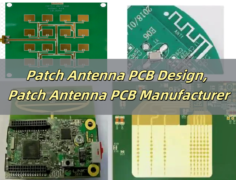
What is a Patch Antenna PCB?
A patch antenna PCB is a specialized type of antenna that is commonly used in wireless communication devices. It consists of a flat, rectangular, or square metal patch mounted on a printed circuit board (PCB) with a dielectric substrate between the patch and a ground plane. Due to their directional nature, patch antennas radiate energy in a specific direction rather than all around, which makes it efficient for applications that require focused signal transmission.
The patch antenna PCB is widely chosen for its lightweight structure, and ease of integration into various applications. Unlike traditional antennas with bulky components, patch antennas offer a streamlined solution for devices requiring high-frequency transmission. Industries such as telecommunications, aerospace, automotive, and consumer electronics rely on patch antennas for their wireless networking needs.
What Does a Patch Antenna PCB Do?
A patch antenna PCB functions as a key component in wireless communication systems. It serves the purpose of sending and receiving radio frequency (RF) signals in a controlled manner. When an electric current is supplied to the antenna, it generates electromagnetic waves that propagate through the air. The same process works in reverse when receiving signals.
Patch antennas are extensively used in various applications, including:
- Wi-Fi Networks – Routers and access points.
- Bluetooth Devices – Wireless headsets, speakers, and IoT devices.
- GPS Systems
- RFID Applications – Retail and logistics industries.
- Satellite-based Communications
The effectiveness of a patch antenna PCB largely depends on its design, material, and positioning. When correctly engineered, it delivers high efficiency, strong gain, and minimal signal loss, providing a reliable performance in various environments. If you have similar designs while looking for an experienced patch antenna PCB manufacturer, just feel free to reach us at sales@bestpcbs.com. BEST team is a professional PCB supplier who providing turn-key patch antenna PCB service, including layout, design, manufacturing, components sourcing and PCB assembly. To ensure service, our company has established rapid-response and one-to-one after sale service teams, there is no worry for you!
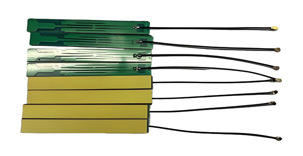
Patch Antenna PCB Types
Patch antenna PCBs can be divided into different types according to its function and specifications, each designed to suit different frequency ranges and applications. Here are some of the most commonly used types:
1. Standard Patch Antennas
These are the basic patch antennas used in general wireless communication. They provide good performance for short- and medium-range applications.
2. 2.4 GHz Patch Antenna PCB
Designed specifically for the 2.4 GHz frequency band, they are widely used in Wi-Fi, Bluetooth, and IoT applications. This kind of patch antenna PCB provides stable signal transmission with minimal interference.
3. Dual-Band Patch Antennas
These antennas operate on two frequency bands, such as 2.4 GHz and 5 GHz, making them suitable for devices that require dual-band connectivity, such as modern Wi-Fi routers and mobile communication systems.
4. Circular Polarized Patch Antennas
Circular polarization enhances signal reception by reducing signal degradation due to environmental factors. These antennas are preferred in satellite communication, RFID, and drone applications.
5. GPS Patch Antennas
GPS patch antenna PCBs are optimized for frequencies used in satellite navigation and position systems. They provide accurate location tracking with high precision, always exist in our mobile phones, laptops, vehicle cars and so on.
What is the Best Substrate for a Patch Antenna PCB?
The substrate material affects the performance of a patch antenna PCB. High-frequency applications require materials with low dielectric loss and stable electrical properties. Common choices include Rogers RT Duroid, Taconic, and FR4.
- While FR4 is cost-effective and relative dielectric constant is generally between 4.0-4.5, it is always used in general wireless communication devices.
- The dielectric constant of different types of Rogers substrates can be selected between 2.2-10, and are commonly used in high frequency antenna designs, such as millimeter wave antennas, satellite communication antennas, etc.
- Taconic substrate has a low dielectric constant, which can reduce the delay and distortion of signal propagation, and is conducive to the transmission of high-frequency signals. Suitable for high frequency band applications such as millimeter wave.
GPS Patch Antenna PCB Design Guide
GPS patch antenna PCB design requires careful planning to achieve high precision and reliability. GPS antennas operate at specific frequencies, typically 1.575 GHz (L1 band) and 1.227 GHz (L2 band), meaning the design must ensure accurate impedance matching, minimal signal loss, and strong gain.
1. Selecting the Right Substrate Material
For high-performance GPS antennas, Rogers RO4000 or ceramic-based substrates are recommended due to their low dielectric loss and stability at high frequencies. Here is a comparison between each material’s performance.
| Material | Dielectric Constant (εr) | Advantages |
| Rogers RO4000 Series | 3.38 – 3.55 | Low loss, stable performance, good for high-frequency designs. |
| Teflon (PTFE) | 2.1 | Excellent performance, minimal signal loss, ideal for precision applications. |
| Ceramic-Based Substrates | 6 – 10 | High dielectric constant, small form factor, suitable for embedded GPS antennas. |
| FR4 | 4.4 | Low cost but has higher signal loss, suitable for less critical applications. |
2. Patch Antenna Geometry & Dimensions
The size of the patch directly affects the operating frequency. The patch length and width are calculated using the resonant frequency formula:

Where:
- L = Patch length
- c = Speed of light (3 × 10⁸ m/s)
- f = Operating frequency (1.575 GHz for GPS L1)
- εr = Dielectric constant of the substrate
Following typical GPS patch antenna dimensions rule as below:
- Patch Length (L): ~25mm for L1 frequency
- Patch Width (W): ~25mm
- Substrate Thickness: 1.6mm – 2.5mm for optimal performance
These dimensions may vary based on substrate material and desired bandwidth.
3. Impedance Matching and Feed Methods
A well-matched GPS patch antenna typically has an impedance of 50Ω for maximum signal transfer. Mismatch leads to signal reflection, reducing efficiency.
Common Feeding Methods:
- Microstrip Line Feed – Uses a thin transmission line to connect the patch to the circuit.
- Coaxial Probe Feed – A coaxial cable is directly soldered to the patch.
- Inset Feed – A small cut in the patch optimizes impedance matching.
- Proximity Coupling Feed – A dielectric layer separates the patch and feed line.
Impedance Matching Techniques:
- Adjusting the patch dimensions.
- Using a quarter-wave transformer for gradual impedance transition.
- Employing matching networks such as capacitors or inductors.
4. Ground Plane Optimization
The ground plane should be at least twice the size of the patch to reduce edge effects. To maintain signal stability, you can use a solid ground layer instead of split or partial ground. Additionally, avoid placing components close to the patch to reduce interference. Please noted that: a larger ground plane improves gain, while a smaller ground plane can degrade performance.
5. Circular Polarization for GPS Antennas
GPS signals are circularly polarized, meaning the antenna must support circular polarization for better reception. To achieve a circular polarization, try to use below methods:
- Corner Truncation: Cutting two opposite corners of the patch to create phase shift.
- Dual Feed Method: Feeding the patch at two orthogonal points with a 90° phase difference.
- Slot Loading: Adding slots in the patch to modify current distribution.
6. Placement and Orientation Considerations
The position of the GPS patch antenna affects signal reception.
- Place the antenna on top of the PCB, away from interfering components.
- Orient the patch facing upwards for direct satellite signal reception.
- Keep at least 10mm clearance around the antenna to minimize obstructions.
For wearable or mobile applications, placing a ground plane behind the antenna improves performance by reflecting signals.
7. Testing and Tunning the GPS Patch Antenna
Once the PCB is designed, thorough testing ensures it meets performance expectations. Here are some testing that Best Technology always used:
- Return Loss Measurement: A Vector Network Analyzer (VNA) verifies impedance matching.
- Antenna Gain Testing: Determines signal strength and coverage.
- Radiation Pattern Analysis: Ensures directional characteristics align with design specifications.
- GPS Receiver Performance Testing: Evaluates signal lock speed and accuracy in real-world conditions.
Hope this guide make you sense! If you need custom GPS patch antenna PCBs, Best Technology provides high-precision fabrication, top-quality materials, and expert support for your high-performance GPS patch antennas suitable for various applications, including navigation systems, IoT devices, and autonomous vehicles. Contact us today to discuss your project!
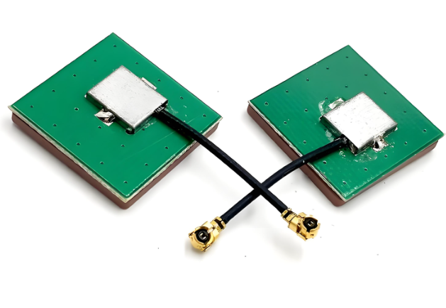
How to Separate Two Patch Antennas on a PCB?
When designing a PCB with multiple patch antennas, proper isolation is crucial to prevent signal interference. Some effective techniques include:
- Keeping antennas at least half the wavelength apart minimizes unwanted coupling.
- Placing a grounded metal plane between antennas reduces cross-talk.
- Metallic enclosures or RF shielding materials help further isolate signals.
How to Install a Patch Antenna PCB on Your Device?
Proper installation is key to ensuring that a patch antenna PCB functions as intended. Follow these steps for optimal results:
- Select the Ideal Placement
- Position the antenna in an open space to minimize obstructions.
- Avoid placing it near metal components that may interfere with signals.
- Secure the PCB Firmly
- Use adhesive or screws to keep the PCB stable.
- Ensure there is no movement that could affect signal reception.
- Connect the Feed Line Properly
- Solder the feed line securely to prevent connectivity issues.
- Use impedance-matched connectors for reduced signal loss.
- Test Performance
- Measure signal strength using an RF analyzer.
- Adjust positioning if needed for better reception.
Following these steps, you can install a patch antenna PCB to your devices. If you still have some questions about installation methods, you are welcome to leave message on the comments.
Why Choose Best Technology as Your Patch Antenna PCB Manufacturer?
If you are looking for a reliable patch antenna PCB manufacturer, Best Technology stands out. We are a one-stop PCB vendor in Asia, that offering high-quality solutions tailored to various applications. Here’s why customers trust us:
- We use industry-leading substrates like Rogers and Teflon for superior signal performance.
- We have stable substrate supply chain and most reasonable price to save your money.
- Our engineers work closely with clients to develop customized antenna solutions.
- Our factory equipped with advanced manufacturing machines, ensuring reliable, high-efficiency antennas.
- Rigorous testing guarantees compliance with industry standards.
- ISO13485, ISO9001, IATF16949, AS9100D certificated.
- With 18+ years of expertise, we provide technical guidance for every project.
- Expedited service provided to meet your time-sensitive orders.
- 5 years quality assurance, you can contact our sales every time if products have quality issue.
- DDP & DDU quotation available to cover part of tariff.
If you’re looking for a trusted manufacturer to deliver high-performance patch antenna PCBs, Best Technology is your ideal choice. Contact us today to discuss your needs!
You may also like


Tags: 2.4 ghz patch antenna pcb, gps patch antenna pcb design, patch antenna pcb, pcb patch antenna