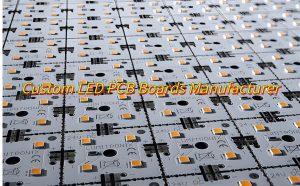
Would you like to know how to reduce production cost of aluminum backed PCB? Let’s explore more about aluminum backed PCB’s structure, applications, prototyping process. and how to select a OEM aluminum backed PCB manufacturer as well as how to reduce production cost.
Best Technology focus on aluminum backed PCB one stop solution over 18 years. We accelerate project timelines with 48 hours rapid prototyping, enabled by automated laser drilling and 24/7 thermal lamination lines. Our multi-layer aluminum PCB capabilities (up to 6L, ±0.05mm tolerance) resolve complex thermal management challenges in EV battery modules and high-power LEDs. A dedicated engineer team provides 1:1 DFM analysis and real-time prototyping support, slashing design-to-production errors by 40%. Clients benefit from 98% on-time delivery rates and NPI cost reductions up to 30% through material optimization strategies. Contact us today if you have any request for aluminum backed PCBs: sales@bestpcbs.com
What Is Aluminum Backed PCB?
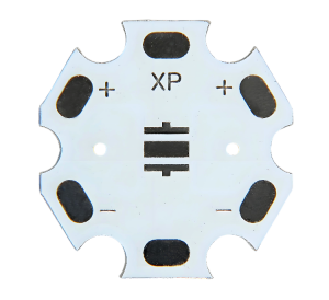
An Aluminum Backed PCB (Aluminum Based Printed Circuit Board) is a specialized circuit board that integrates a high-thermal-conductivity aluminum alloy substrate as its core layer. This design replaces traditional FR-4 or ceramic substrates with aluminum, offering superior heat dissipation capabilities while maintaining electrical functionality. The structure typically includes a thermally conductive dielectric layer between the aluminum base and a copper circuit layer, enabling efficient transfer of heat away from power components. Aluminum-backed PCBs are widely used in applications requiring robust thermal management, such as LED lighting, power electronics, automotive systems, and industrial controls, where they enhance reliability and extend device lifespan by preventing overheating.
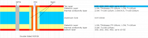
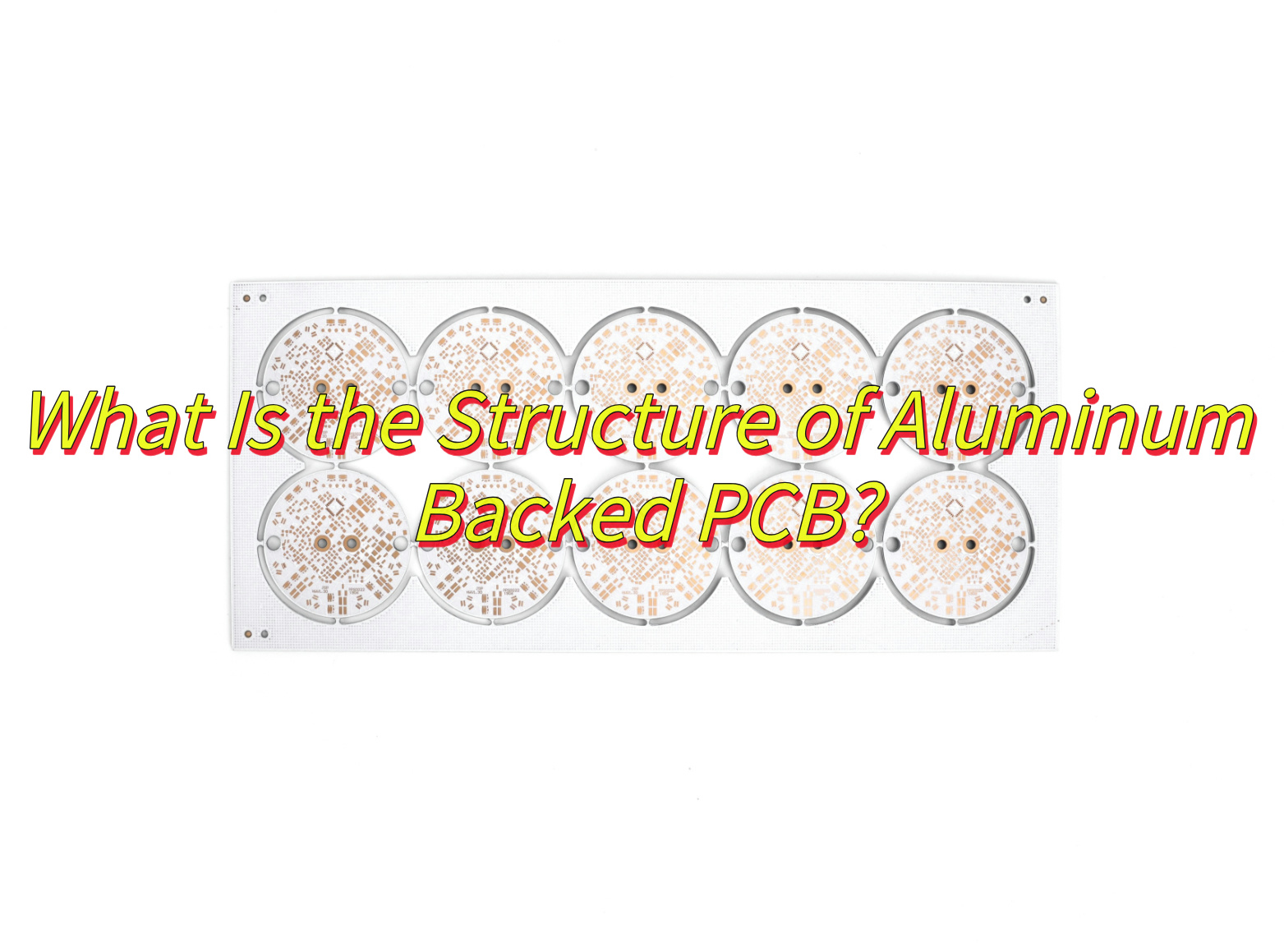
What Is the Structure of Aluminum Backed PCB?
Here are the structure of Aluminum Backed PCB:
1. Circuit Layer (Copper Foil)
- Material: Electrolytic copper foil (1–10 oz thickness) optimized for high-current applications.
- Function: Forms conductive pathways through precise etching, supporting component mounting and signal routing.
2. Thermally Conductive Dielectric Layer
- Composition: Polymer-ceramic hybrid insulation (e.g., epoxy resin with ceramic fillers) with UL-certified thermal conductivity.
- Thickness: 0.075–0.15 mm, balancing electrical isolation and heat transfer efficiency.
- Property: Low thermal resistance (as low as 0.15°C/W) to rapidly channel heat from components to the base.
3. Metal Base Layer (Aluminum Substrate)
- Material: Aluminum alloy (1–3 mm thickness) or copper for extreme thermal demands.
- Durability: Resists mechanical stress in high-vibration environments (e.g., automotive electronics).
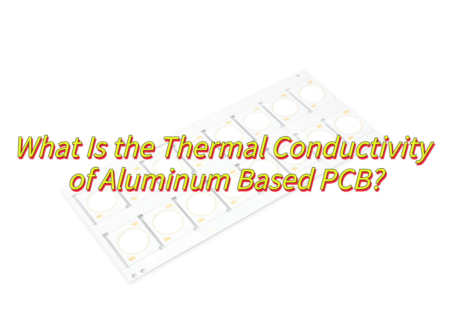
What Is the Thermal Conductivity of Aluminum Based PCB?
Here are thermal conductivity of aluminum based PCB:
- Dielectric layer: Polymer-ceramic hybrid insulation (e.g., epoxy with alumina fillers) typically provides 1–2W/m·K in standard designs. Advanced composites with aluminum nitride (AlN) or optimized ceramic networks can exceed 5W/m·K, enhancing heat transfer efficiency.
- Aluminum substrate: Pure aluminum contributes ≈200W/m·K, but its full potential is constrained by the dielectric layer’s thermal resistance.
- Structural innovations: Textured aluminum surfaces and groove-embedded dielectric interfaces reduce thermal impedance, achieving up to 8.5W/m·K in high-performance variants.
What Are the Application of Aluminum Based PCB?
Application of aluminum based PCB board:
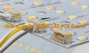
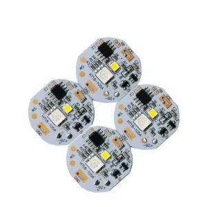
- LED Lighting:High-power LED modules, streetlights, and automotive headlights, where efficient heat dissipation prevents thermal degradation and extends lifespan.
- Power Electronics:Inverters, converters, and power supplies for renewable energy systems (solar, wind), electric vehicles, and industrial motor drives.
- Automotive Industry:Engine control units (ECUs), battery management systems (BMS), and hybrid/electric vehicle components requiring robust thermal management.
- Consumer Electronics:High-performance devices like audio amplifiers, telecom modules, and gaming hardware, where compact form factors and heat control are critical.
- Industrial Controls:Variable frequency drives (VFDs), servo motors, and robotics systems, where reliability under heavy loads and high temperatures is essential.
- Medical Devices:Imaging equipment (MRI, CT scanners), laser systems, and wearable healthcare monitors, demanding precise thermal regulation for sensitive components.
- Aerospace & Defense:Avionics, radar systems, and satellite electronics, where weight reduction and thermal stability in harsh environments are priorities.
- HVAC Systems:Energy-efficient heating, ventilation, and air conditioning units, utilizing aluminum PCBs for compact, high-power control circuits.
- Telecommunications:Base stations, routers, and network switches, where thermal management ensures stable operation under continuous high-load conditions.
- Renewable Energy: Solar inverters, wind turbine controllers, and energy storage systems, benefiting from aluminum PCBs’ lightweight and high-thermal efficiency.

What Is Prototyping Process of Aluminum Backed PCB?
This is the prototyping process of aluminum backed PCB:
1. Design Validation & Material Selection
- Thermal Simulation:
Use tools (e.g., ANSYS) to model heat dissipation. Validate aluminum substrate thickness (1.0–3.2 mm) and dielectric layer (100–200 µm) for thermal requirements. - Layer Stack-up Design:
Define copper layers, dielectric, and aluminum core based on current capacity and thermal resistance targets. - Component Placement:
Position high-power components on the aluminum side for direct heat spreading.
2. Fabrication of Prototype
- Material Preparation:
- Aluminum Substrate: Choose thickness (1.0–3.2 mm) and alloy (e.g., 6061-T6 for thermal conductivity 1–4 W/m·K).
- Dielectric Layer: Use high-TG materials (e.g., FR-4, polyimide) for reliability.
- Layer Lamination:
Press copper foil, dielectric, and aluminum core under heat/pressure to bond layers. Ensure adhesion strength >9 lb/in. - Drilling & Plating:
Create via holes for interlayer connections and plate with copper (25–50 µm) using electroless or electrolytic methods.
3. Circuit Patterning & Etching
- Photo Imaging:
Apply dry film or liquid photoresist, expose via photomask, and develop to reveal the circuit pattern. - Etching:
Remove excess copper using acid (e.g., ferric chloride) or alkaline solutions, leaving traces (1–3 oz/ft²).
4. Solder Mask & Surface Finish
- Solder Mask Application:
Coat with liquid photo-imageable solder mask (LPI) to protect traces and define solderable areas. - Surface Finish:
Apply ENIG, HASL, or OSP for solderability and corrosion resistance.
5. Assembly & Testing
- Component Mounting:
Solder components (e.g., LEDs, MOSFETs) using reflow or wave soldering. - Thermal Testing:
Measure junction-to-ambient thermal resistance (θJA) to ensure it meets specifications (e.g., <20°C/W for LEDs). - Electrical Testing:
Perform flying probe or in-circuit testing (ICT) to verify signal integrity and continuity.
6. Iteration & Optimization
- Failure Analysis:
Use X-ray inspection or cross-sectioning to identify defects (e.g., voids, delamination). - Design Adjustments:
Modify trace widths, via sizes, or materials based on test results to improve performance or manufacturability.
How to Select An OEM Aluminum Backed PCB Manufacturer?
This is how to choose an OEM aluminum backed PCB manufacturer:
Verify Material Expertise
- Confirm use of ≥1.0W/m·K thermal conductivity dielectric layers (epoxy-ceramic hybrids) and 1–3mm aluminum substrates for heat management.
- Check availability of blue solder mask options for improved thermal reflection in LED applications.
Assess Technical Capabilities
- Prioritize manufacturers offering 16+ layer HDI PCB fabrication for complex designs requiring embedded components or fine-pitch traces.
- Ensure SMT assembly integration with ≤0.3mm component placement accuracy for high-density layouts.
Evaluate Customization Flexibility
- Require free OEM samples with ≤72-hour lead times to test mechanical/thermal performance.
- Confirm support for non-standard aluminum core shapes (grooved/textured) to enhance heat dissipation.
Audit Quality Control
- Demand IPC-A-610 Class 3 certification for aerospace/medical-grade reliability.
- Verify in-house thermal cycling tests (-40°C to +150°C) and isolation resistance (>10MΩ) validation.
Review Supply Chain Transparency
- Choose suppliers with secured component sourcing networks to mitigate material shortages.
- Confirm real-time production tracking and ≤48-hour response times for design revisions.
How to Reduce Production Cost of Aluminum Backed PCB?
Strategies to Reduce Aluminum Backed PCB Production Costs:
Material Optimization
- Use standardized aluminum core thicknesses (e.g., 1.5mm instead of custom 1.2mm/3.0mm) to minimize raw material waste.
- Replace pure aluminum (5052/6061) with lower-cost aluminum composites (Al-Fe-Si alloys) where thermal demands allow.
Design Simplification
- Eliminate unnecessary vias and reduce layer count (single-layer instead of double-layer) unless electrical isolation mandates complexity.
- Standardize solder mask colors (white/green) instead of custom hues like blue/black.
Process Efficiency
- Batch-process multiple PCB designs on shared aluminum panels (≥80% material utilization).
- Replace laser cutting with chemical etching for non-critical edge profiles.
Supplier Negotiation
- Secure bulk discounts by consolidating dielectric prepreg orders across projects.
- Partner with local aluminum suppliers to cut logistics costs (≥12% savings).
Test Optimization
- Limit thermal cycling tests to 50 cycles (-40°C/+125°C) unless aerospace/medical standards require 100+ cycles.
- Use automated optical inspection (AOI) instead of manual checks for solder joint validation.
What Is the Price of Aluminum Backed PCB?
The price of aluminum-backed PCBs (Aluminum PCBs) typically ranges from $2 to $50 per unit, depending on several main factors:
- Material Specifications: Higher-grade aluminum substrates, specialized dielectric layers (e.g., high thermal conductivity), and thicker copper layers increase costs.
- Design Complexity: Multi-layer boards, tight trace/spacing tolerances, and advanced hole features (e.g., microvias) drive up manufacturing expenses.
- Order Volume: Larger quantities generally qualify for volume discounts, reducing unit prices.
- Additional Requirements: Specialized surface finishes, testing (e.g., thermal cycling), or compliance certifications (e.g., UL, RoHS) add to the final cost.
- Market Conditions: Fluctuations in aluminum and copper prices directly impact raw material costs, while geographic location and lead time requirements (e.g., expedited production) can also affect pricing.
In summary, that’s all about aluminum backed PCB’s structure, applications, prototyping process. and how to select a OEM aluminum backed PCB manufacturer as well as how to reduce production cost. If you have any issues about aluminum based PCB, welcome to leave a message below this blog.