
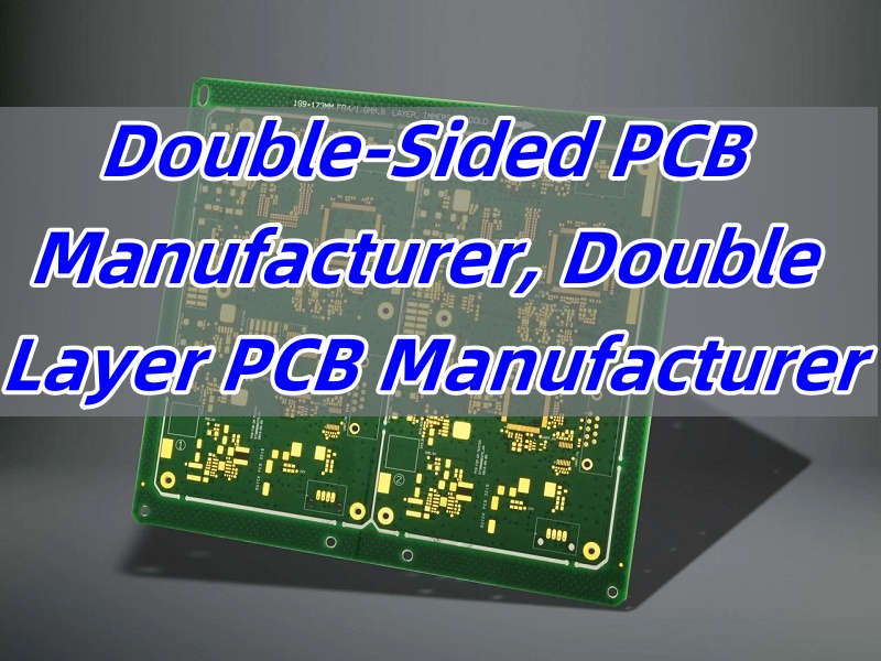
Double-sided PCB manufacturer is a phrase you’ll come across when sourcing dependable circuit boards. Whether you’re building compact electronics or advanced control panels, these boards are the backbone. However, choosing the right manufacturer isn’t always easy. In this blog, we’ll walk you through essential points like how they’re made, where they’re used, and how to find the best one.
Best Technology is a professional double-sided PCB manufacturer, who always deliver consistently on time. There is 97% on-time delivery rate across 40 countries by Best Technology. We have advanced inspection technology used in double-sided PCB manufacturing processes, such as Automated optical inspection (AOI), 3D X-ray tomography for BGA voiding analysis, and In-circuit testing (ICT) fixtures for 100% functional validation. We support 24/7 engineering support with 2-hour DFM feedback. Best Technology has possessed AS9100D aerospace certification, IATF 16949 automotive QMS.
Whether you require double-sided PCB design guidance, double-sided PCB prototype development, double-sided PCB fabrication, or full-scale double-sided PCB assembly solutions, our team is available to address your needs at any time. A warm welcome to contact us via sales@bestpcbs.com to discuss your specific needs for double-sided PCB.
What is a Double-Sided PCB?
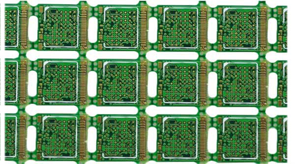
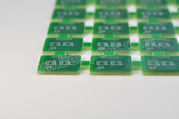
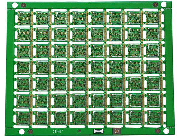
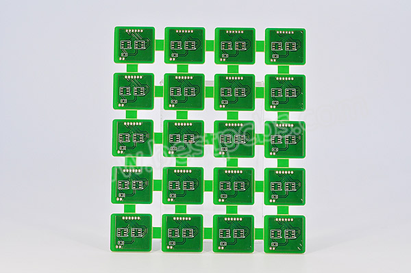
A double-sided PCB is also called a double-layer PCB. It has copper traces on both sides connected through vias, allowing component placement on either surface. As a cost-effective solution between single-sided and multilayer PCBs, it provides 60% higher wiring density than single-layer boards. These PCBs are widely used in consumer electronics (e.g., smartphone motherboards), automotive controls, and industrial automation systems, balancing performance and manufacturing costs.
How Are Double-Sided PCBs Manufactured?
Double-sided PCB manufacturers follow a series of precise and professional steps to produce reliable circuit boards. At Best Technology, we use a proven process designed to ensure performance, quality, and consistency. Here’s how we do it:
1. CAM Engineering Processing
- It all starts with careful design file preparation. Our CAM engineers review Gerber files, optimize them, and ensure everything is ready for manufacturing. They prepare the data used throughout the production line.
2. Drilling (Mechanical or Laser Drilling)
- Next, we drill holes for vias and through-hole components. Depending on the design, we use either mechanical drills or laser drilling methods. This step lays the foundation for reliable connections between the two copper layers.
3. Hole Metallization (Chemical Copper Plating → Electroplating)
- Once drilling is done, we chemically deposit a thin layer of copper inside the holes. This is followed by electroplating to thicken the copper, which creates conductive paths between layers.
4. Outer Layer Pattern Imaging (Lamination → Exposure → Developing)
- Here, we apply a photosensitive dry film on the board and expose it to UV light through a photo-tool. After developing, the unexposed areas are removed, revealing the copper that will form the final circuit pattern.
5. Pattern Plating (Copper + Tin)
- We then plate the exposed copper with a thicker layer of copper, followed by a tin layer to protect it during the next etching step. This builds up the conductive traces to the right thickness.
6. Etching (Film Removal → Etching → Tin Stripping)
- After plating, we strip off the photoresist. Then we etch away the unwanted copper. The tin layer acts as a barrier and is later removed, leaving behind clean copper traces.
7. Solder Mask Application (Coating → Exposure → Developing)
- We apply a green solder mask to protect the copper circuitry. The board is exposed again to define areas where components will be soldered, then developed to wash away the excess.
8. Surface Finishing (ENIG, HASL, OSP, etc.)
- Now it’s time for surface treatment. We apply finishes like ENIG (Electroless Nickel Immersion Gold), HASL (Hot Air Solder Leveling), or OSP (Organic Solderability Preservative). These enhance solderability and prevent oxidation.
9. Mechanical Profiling (Routing/V-Cut/Punching)
- Boards are shaped and separated using different techniques like milling, V-cutting, or punching. This step ensures the board fits perfectly into its final application.
10. Electrical Testing & Final Inspection (AOI/Flying Probe/Impedance Testing)
- Finally, each board undergoes full electrical testing using AOI (Automated Optical Inspection), flying probe tests, and impedance checks. Our team performs a final inspection to ensure every board meets strict quality standards.
This detailed process ensures every double-sided PCB from Best Technology is dependable, high-quality, and ready for advanced applications.
How Do You Make a Double Layer PCB?
Double Layer PCB is also named Double Sided PCB. The Double Layer PCB manufacturing process is the same as above double sided PCB manufacturing process listed. As a leading double layer PCB manufacturer, we are happy to provide quick double layer PCB manufacturing service to you.
How Are Double-Sided PCBs Soldered?
Double sided PCB soldering uses different techniques depending on component types. If both sides have surface-mount devices (SMD), one side is reflow soldered first. Then, the second side is processed with care to avoid disturbing the first.
Through-hole components usually go through wave soldering. For mixed assemblies, selective soldering is used to avoid reworking finished parts. Skilled operators or automated machines handle the job. Quality checks follow to catch defects.
Double sided PCB assembly is a key part of this process. Good manufacturers use AOI (automated optical inspection) and sometimes X-ray to ensure quality.
How Much Does a Double-Sided PCB Manufacturer Charge for Custom Boards?
Pricing depends on several factors:
- Board size and quantity
- Copper weight and layer thickness
- Hole count and via complexity
- Solder mask color, surface finish
- Lead time and testing
A custom board might start from a few dollars each for small runs, but the price drops with higher volumes. Always ask for a quote based on your actual Gerber files. A reliable double-sided PCB manufacturer will also offer suggestions to cut costs.
What is the Best PCB Manufacturer?
Finding the best double-sided PCB manufacturer is a key step when quality, turnaround time, and budget all matter. India has become a growing hub for PCB production due to its skilled labor and advanced factories. Here’s a brief overview of some trusted manufacturers based in India.
Top 5 Double Sided PCB Manufacturers in India:
AT&S India Pvt. Ltd.
- One of the leading PCB manufacturers globally, AT&S operates a large plant in Nanjangud. They serve automotive, medical, and industrial electronics. Their processes meet strict European standards.
Genus Electrotech Ltd.
- Located in Gujarat, Genus offers end-to-end PCB fabrication and assembly services. Their facility supports double-sided and multi-layer PCB production with a strong domestic presence.
Shogini Technoarts Pvt. Ltd.
- This Pune-based company specializes in quick-turn PCB solutions and has decades of experience. They cater to medium and high-volume orders with reliable customer service.
Fine-Line Circuits Ltd.
- A Mumbai-based exporter of double-sided and multilayer PCBs, they serve the aerospace, industrial, and telecom markets. Their consistent export quality makes them a preferred choice overseas.
CIPSA-TEC India Pvt. Ltd.
- CIPSA-TEC runs a well-equipped plant in Bangalore. They provide single, double, and multi-layer boards with lead-free processes and strong quality control.
These companies have invested in modern equipment, skilled engineers, and global certifications. That means you get better quality and support at competitive pricing. India’s PCB manufacturing industry is growing fast. Whether you need a simple double-layer board or a complex assembly, these manufacturers have the resources. Comparing capabilities and support is crucial. Always ask for samples, visit facilities if possible, and go with the one that best fits your project’s needs.
How to Choose a Reliable Double-Sided PCB Manufacturer?
Choosing a double-sided PCB manufacturer goes beyond browsing websites. Look for the following signs of a reliable partner:
- Clear communication and fast response
- Transparent pricing
- Quality management system in place
- Samples available before bulk orders
- Engineering support for layout review
Check if they’ve worked in your industry. A factory that supplies boards for automotive controls may not be ideal for LED lighting. The right match saves you time and stress.
What Are the Typical Applications Served by a Double-Sided PCB Manufacturer?
Double-sided PCB applications are found everywhere. Here are a few areas where they are commonly used:
- Consumer Electronics: Remote controls, toys, smartwatches
- Industrial Controls: Motor drivers, automation circuits
- LED Systems: Light engines, drivers, and power management
- Medical Devices: Compact monitors and diagnostics tools
- Telecom: Signal repeaters, interface modules
These boards fit well between low-cost single sided options and high-end multi-layer PCBs. A good manufacturer will help you pick the right stack-up and material based on your end use.
In conclusion, double-sided PCBs bridge the gap between simplicity and complexity. When you work with a reliable double-sided PCB manufacturer, you get strong performance and good value. You also save time during design and fewer headaches during production.
Best Technology has more than 18 years of experience as a double-sided PCB manufacturer. We provide one-stop solutions from double-sided PCB prototype to double-sided PCB mass production. With a strict quality system, fast lead times, and responsive support, we’re ready to help with your next project. Just feel free to reach out to us via sales@bestpcbs.com for quick support.
You may also like


Tags: Double Layer PCB Manufacturer, Double-Sided PCB Manufacturer