
Are you looking for LED Array PCB solutions? Let’s explore more through this blog about LED array PCB’s advantages, basic layout rule, optimization design and cost reduction solution, manufacturing process so on.
At Best Technology, we specialize in LED Array PCB solution from design to manufacturing over 18 years. We deliver strict IP protection (NDA agreements and encrypted R&D processes) and modular designs. Supported by integrated DFM analysis and EMC testing, we promise one-time prototyping success. We have a stable electronic supply chain who can provide you very fast delivery at competitive price.(48-72 hours delivery time for urgent orders). Are you ready to bring your LED array ideas to life? Contact us for a quote: sales@bestpcbs.com
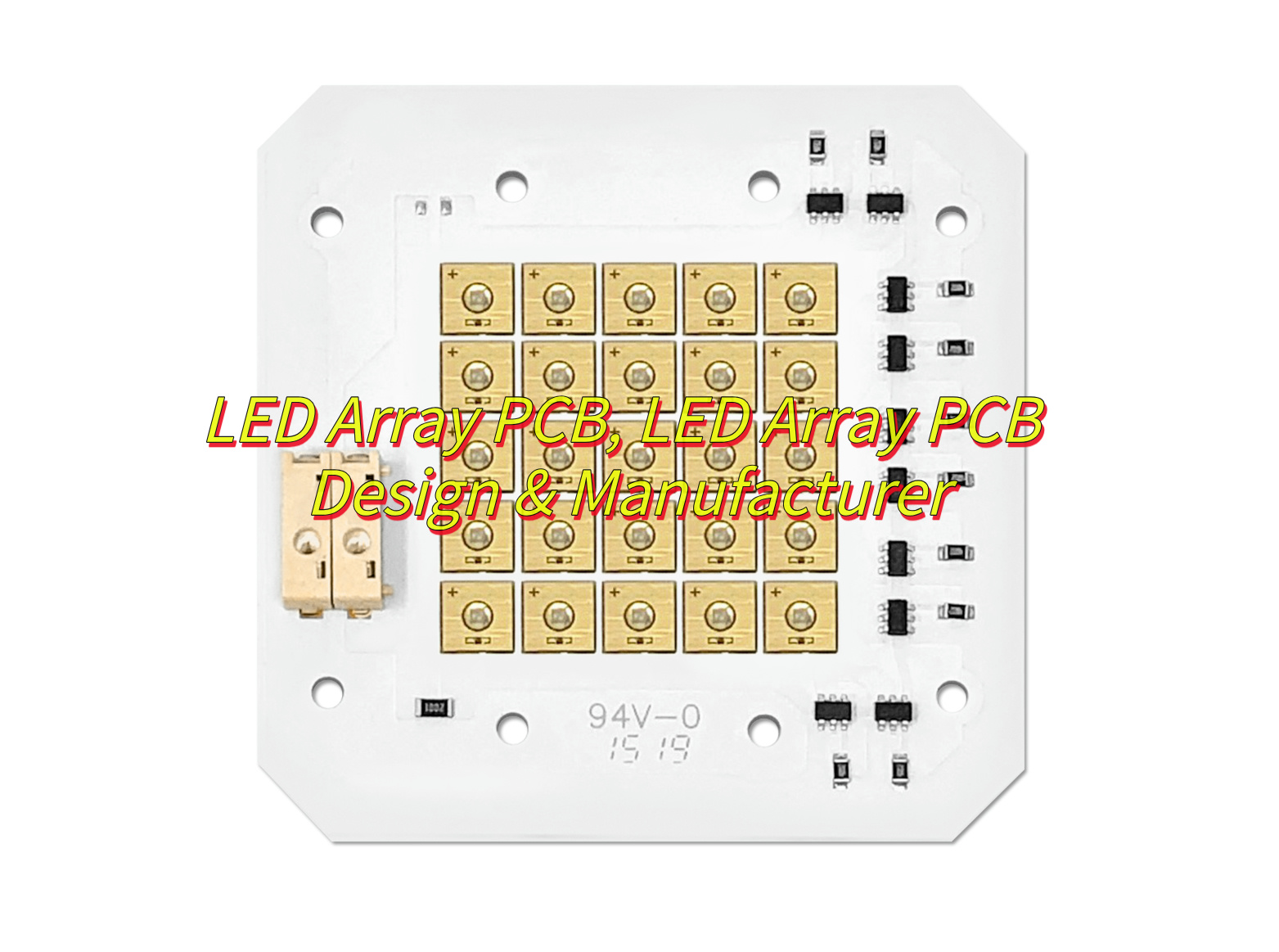
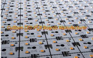
What Is LED Array PCB?
An LED array PCB is a specialized printed circuit board designed to mount and interconnect multiple LEDs in a structured layout. These boards are engineered to control the electrical signals that power the LEDs, enabling precise control over lighting effects such as brightness, color, and patterns.
What Advantages of PCB For LED Array?
- Efficient Thermal Management-PCBs (especially metal-core or ceramic types) dissipate heat effectively, preventing LED overheating.
- Mechanical Stability-PCBs provide robust support for LEDs, protecting them from vibration or physical stress.
- Reliable Electrical Connections-PCBs ensure secure, low-resistance pathways for power and control signals.
- Design Flexibility-PCBs enable complex circuit layouts for LED control, dimming, and color mixing.
- Scalable Manufacturing-PCBs support high-volume production with consistent quality and lower per-unit costs.

Why Choose Infrared LED Array PCBs?
Here’s a list of reasons to choose an infrared LED array PCB:
- Enhanced Thermal Management–IR LEDs often run hot; PCBs (especially metal-core) improve heat dissipation.
- Precise Optical Control-PCBs enable narrow-beam or wide-angle IR emission patterns via layout design.
- Efficient Energy Use-PCBs optimize circuit paths to minimize power loss in IR applications.
- Compact Integration–PCBs allow dense IR LED placement for high-intensity output in small spaces.
- Wavelength-Specific Design–PCBs can be tailored for specific IR wavelengths (e.g., 850nm or 940nm) for sensors/cameras.
- Cost-Effective Scaling-PCBs support high-volume IR LED production with consistent performance.
- Improved Signal-to-Noise Ratio–PCBs reduce electromagnetic interference (EMI) for clean IR data transmission.
- Uniform Light Distribution–PCBs enable even spacing and alignment of IR LEDs for consistent illumination.
What Are the Basic Rules of LED Array PCB Layout?
Here are basic rules of LED array PCB design layout:
Thermal Management Priority
- High-Thermal Substrates: Use aluminum (≥200 W/m·K) or copper (≥380 W/m·K) PCBs to dissipate heat efficiently.
- Copper Pour Placement: Surround LED pads with thick copper layers (≥2oz) to create heat conduction paths.
- Thermal Vias: Add via arrays (0.3mm diameter, 1.5mm spacing) under LEDs to transfer heat to inner layers or heatsinks.
Uniform Current Distribution
- Star Topology Routing: Connect LEDs in parallel with equal-length traces to avoid voltage drop.
- Trace Width Calculation: Size power traces based on current load (e.g., 1A/mm width for SMD LED arrays).
Component Spacing Optimization
- LED Spacing: Maintain ≥3× LED chip size between emitters to prevent thermal coupling.
- Driver Isolation: Place driver ICs ≥5mm away from LEDs to reduce thermal interference.
Signal Integrity Control
- Ground Plane Separation: Split analog/digital ground planes to minimize EMI in mixed-signal designs.
- Shielding: Use guard rings around sensitive traces for PWM-controlled arrays.
Manufacturing Readiness
- DFM Compliance: Follow IPC-2221 standards for pad sizes and solder mask clearances (≥0.1mm).
How to Optimize the Thermal Design of LED Array PCB?
Here are some optimizing thermal solutions for LED array PCB design:
1. Material Selection
- Substrate: Use aluminum or ceramic PCBs with thermal conductivity >2 W/m·K.
- Copper Layer: Prioritize for 2-4 oz copper thickness to enhance heat spreading.
2. Thermal Via Design
- Via Array: Place dense vias (≥0.3mm diameter, ≤1.5mm pitch) under hotspots.
- Via-in-Pad: Implement for high-power LEDs to reduce thermal resistance by 30-50%.
3. Heat Sink Integration
- Direct Bonding: Attach external heat sinks using thermal epoxy (e.g., Bergquist GAP PAD).
- Fin Geometry: Use extruded aluminum fins with ≥15 fins/inch and ≥20mm height for natural convection.
4. Component Layout
- Spacing: Maintain ≥2mm between LEDs to prevent thermal coupling.
- Symmetry: Centralize high-power LEDs to balance heat distribution.
5. Thermal Interface Materials (TIM)
- Conductive Silicone: Apply 0.1-0.2mm thick silicone (e.g., Shin-Etsu X-23-7783) between PCB and heatsink.
- Phase Change Materials: Use for uneven surfaces (e.g., Indium 8.9HF).
6. Testing
- IR Thermography: Validate designs with real-world testing under load.

What Is Manufacturing Process of SMD LED Array PCB?
Here’s a streamlined overview of the SMD LED array PCB manufacturing process:
1. Substrate Preparation
- Material: FR-4, aluminum, or ceramic PCB with 1-2 oz copper.
- Surface Finish: Apply HASL, ENIG, or immersion silver for solderability.
- Patterning: Use laser direct imaging (LDI) for fine-pitch traces (≥6mil).
2. Solder Paste Printing
- Stencil: Stainless steel foil with aperture ratios 1:1 to 1.5:1.
- Paste: Type 3-4 (no-clean) with 89-95% metal content.
- Printer: Speed ≤150mm/s, pressure 40-80N, snap-off 0.5-1mm.
3. SMD LED Placement
- Machine: High-speed chip mounter (≥20,000 CPH).
- Accuracy: ±0.05mm placement, ±0.03mm rotational alignment.
- Nozzle: Use vacuum nozzles with 0.3-0.8mm diameter.
4. Reflow Soldering
- Preheat: 120-150°C (90-120s)
- Soak: 183°C (60-90s)
- Peak: 217-235°C (20-40s)
- Cooling: <3°C/s
- Oven: Forced convection with ±5°C zone uniformity.
5. Cleaning & Inspection
- Cleaning: Use ultrasonic aqueous or semi-aqueous solutions.
- AOI: Automated optical inspection for solder joints, component presence.
- X-Ray: X-ray inspection for BGA/QFN solder quality.
6. Functional Testing
- ICT: In-circuit testing for opens/shorts.
- LED Test: Light output measurement with integrating sphere.
- Thermal Cycling: -40°C to +85°C for 200 cycles (optional).
7. Conformal Coating
- Method: Selective coating using robotic dispensing.
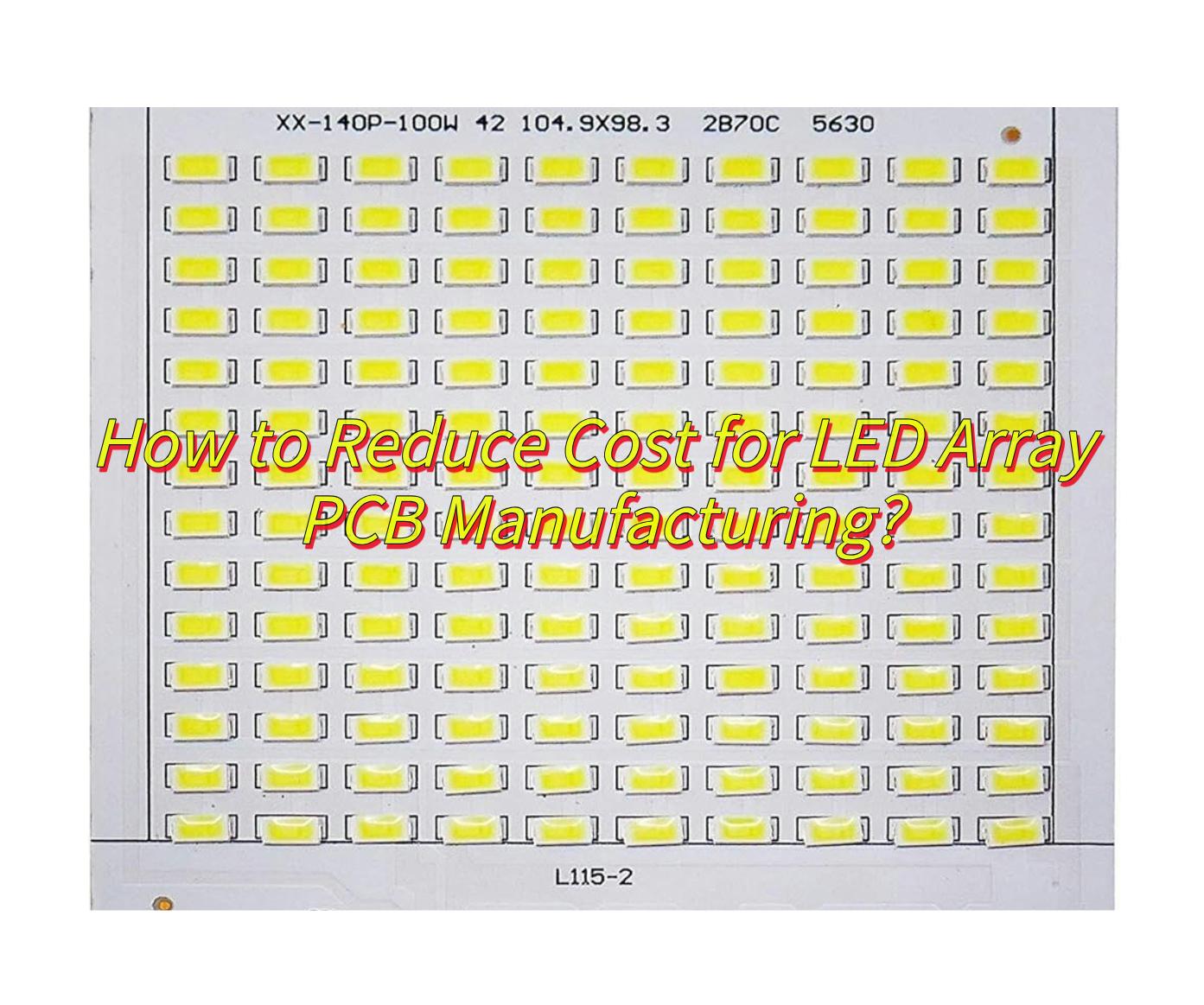
How to Reduce Cost for LED Array PCB Manufacturing?
Here are some ways to how to reduce cost for LED array PCB manufacturing:
- Use cost-effective substrates: Select aluminum-based boards (≥200 W/m·k) instead of ceramic for medium-power arrays (<10W/cm²) to balance thermal performance and material cost .
- Optimize PCB dimensions: Reduce board size by ≥15% through compact LED layout and SMD component conversion while maintaining ≥3mm spacing for depaneling reliability .
- Simplify layer stack–up: Design 2-layer boards with ≥2oz copper instead of 4-layer for standard LED arrays, reducing material costs by ~30% .
- Standardize drill sizes: Use ≥0.3mm vias and ≥0.4mm component holes to avoid precision drilling charges, cutting machining costs by 15-20% .
- Minimize special processes: Avoid gold plating; use HASL surface finish and standard green solder mask to eliminate 25-40% in specialty coating costs .
- Automate assembly: Implement SMT lines with ≥95% first-pass yield, reducing labor costs by 40% compared to manual assembly .
- Strategic sourcing: Partner with PCB manufacturers offering bundled services (design + manufacturing + assembly, like Best Technology) for 10-15% total cost reduction.
FAQs of LED Array PCB Manufacturing
Q1:What materials are typically used in LED array PCBs?
A1:Most LED array PCBs are made with aluminum or other metal core substrates due to their excellent heat dissipation. FR4 can also be used for low-power applications.
Q2:How is heat managed in LED array PCBs?
A2:Heat is managed through thermal vias, metal core bases, and optimized layout design to efficiently transfer heat away from the LEDs.
Q3:What factors affect the brightness and uniformity of an LED array PCB?
A3:Brightness and uniformity are influenced by LED placement, circuit design, current regulation, and quality of the LED components.
Q4:Can LED array PCBs be customized for different lighting applications?
A4:Yes, they can be fully customized in terms of size, shape, LED type, color temperature, and circuit configuration depending on the application (e.g., automotive, signage, medical).
Q5:What are the most common quality control checks during LED array PCB manufacturing?
A5:Common checks include optical inspection, electrical testing, solder joint inspection, and thermal performance evaluation to ensure consistent functionality.
You may also like


Tags: LED Array PCB, LED Array PCB board, LED Array PCB Design