
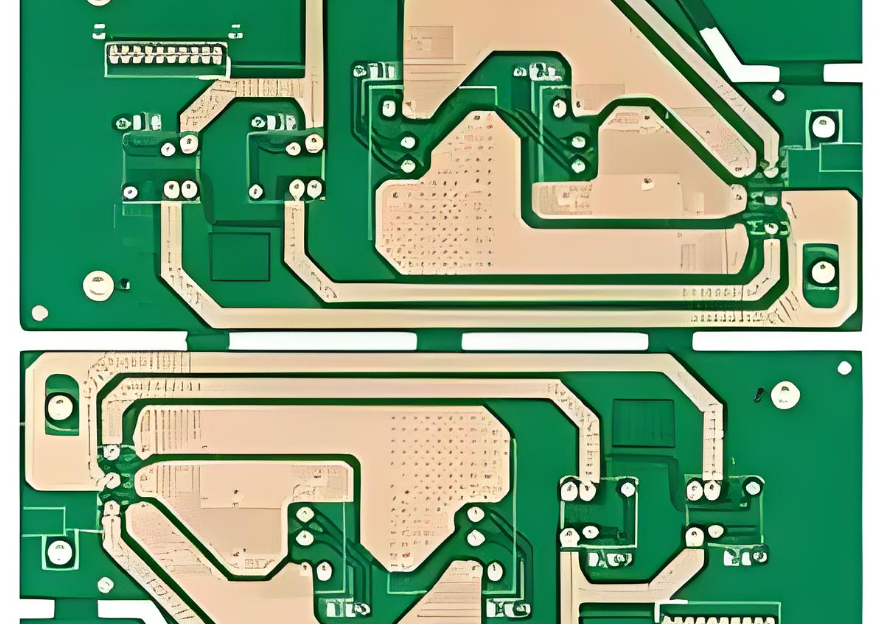
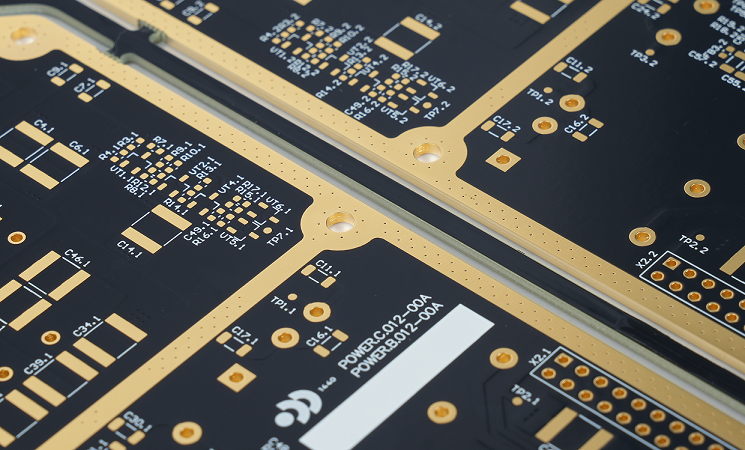
When high-density designs and tight tolerances become the norm, via filling steps in as a reliable technique to elevate performance and reliability. Used in multilayer and HDI PCBs, via filling ensures smooth connections, supports stacked vias, and improves soldering quality.
At Best Technology, we have over 18 years of experience manufacturing advanced PCBs with various via-filling techniques. From BGA designs to microwave circuits, our team supports every step with precision and care. Our factory provides conductive and non-conductive via filling, backed by strict quality inspection and cost-effective solutions. If you’re looking for expert help in via-filled circuit boards, you’re in the right place.
What Is Via Filling in Circuit Boards?
Via filling is a process of inserting a special material into drilled holes (vias) in a PCB layer. These holes, which typically connect one layer to another, are filled with conductive or non-conductive compounds depending on the design. The goal is to create a sealed, flat surface, improve strength, and allow for finer components on the surface—especially important when vias are under BGA or QFN pads.

What Is the Purpose of Via Filling?
Via filling serves both mechanical and electrical purposes. Some key benefits include:
- Supports pad-over-via and via-in-pad designs
- Prevents solder leakage during wave soldering
- Avoids short circuits under fine-pitch components like BGAs
- Prevents flux residue accumulation in vias
- Supports vacuum sealing during in-circuit testing (ICT)
- Prevents solder paste wicking into vias
- Reduces risk of solder ball ejection during wave soldering
- Improves SMT assembly yield and stability
Filled vias are also essential when designing stacked or staggered via structures in HDI boards. Designers often choose via filling when there’s limited space on the board and tight signal routing is needed. It’s common in smartphones, RF modules, and medical devices.
Via Filling Types
Manufacturers use different types of via filling based on the desired outcome and application. Here are the main types:
1. Conductive Via Fill
This method uses conductive materials like silver epoxy or copper paste. It enhances thermal and electrical conductivity. Conductive via fill technique can used in power components or RF signals.
2. Non-Conductive Via Fill
Here, the via is filled with non-conductive epoxy. It seals the hole but does not allow current flow. Commonly used under BGA pads to avoid shorts.
3. Electroplated Copper Filling
In this process, copper is electroplated inside the via, offering unmatched conductivity and strength. It’s the best option for stacked vias but also the most expensive.
4. Resin Plugging
Only one side of the via is filled with resin. It’s a cost-effective solution and most common used that reduces soldering defects but may not offer complete flatness.
5. Tented Vias
This is a basic method where the via is covered, not filled. Dry film solder mask covers the via but doesn’t prevent air pockets or improve flatness.
PCB Via Filling Materials
Choosing the right PCB via filling material depends on whether you need conductive or non-conductive properties. Materials include:
- Silver epoxy (Conductive)
- Copper paste (Conductive)
- Resin-based epoxy (Non-conductive)
- Electroplated copper (Advanced conductive)
At Best Technology, we use reliable via filling compounds sourced from Taiyo, DuPont, and other trusted brands to ensure consistency and performance.
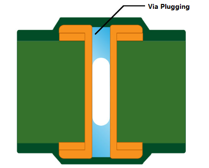
What Is the Difference Between Via Filling and Via Plugging?
In everyday factory usage, some engineers or sales reps might casually use “via plugging” and “via filling” interchangeably, especially when referring to BGA pad designs or HDI boards. However, from a technical and manufacturing standpoint, they serve different functions.
1. Via Plugging
This is the process of partially sealing a via—usually from one side—using non-conductive paste or resin. It’s mainly done to prevent solder wicking during reflow soldering. Plugged vias often remain hollow inside, and are not always planar (flat on the surface).
Key points:
- Seals only one end of the via
- Often used under BGA pads to avoid solder leakage
- Surface may not be flat or planar
- Usually non-conductive paste
- Cheaper and simpler than via filling
2. Via Filling
Via filling, on the other hand, means completely filling the via barrel (the entire hole) with conductive or non-conductive material. The goal is not only to seal but also to create a flat, solid surface for placing components or stacking additional vias on top.
Key points:
- Completely fills the via
- Can be conductive (copper, silver epoxy) or non-conductive
- Enables via-in-pad or stacked via structures
- Supports high-density and multilayer PCB designs
- More complex and costly than plugging
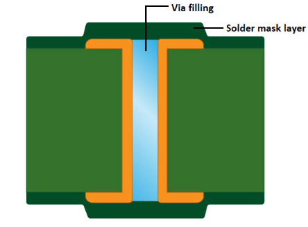
So, if your board design requires a flat surface, thermal transfer, or electrical connectivity, you’re talking about via filling. If you just need to stop solder from leaking through a via, via plugging is enough.
Factors That Affect the Via Filling Cost
The cost of via filling in PCB manufacturing isn’t fixed. It depends on several technical and material-related factors that influence the complexity, time, and resources needed.
1. Via Size and Quantity
The diameter and number of vias play a huge role in overall cost. Smaller vias (like microvias) are harder to fill consistently and require more precision. When you need hundreds or even thousands of vias filled, the time and material usage increases.
- Smaller vias <0.25mm demand tighter control and sometimes special filling equipment.
- More vias mean more PCB via filling material, inspection, and process time.
- Large quantities in high-density areas also increase the chance of defects, which may require rework or careful quality control.
2. Board Thickness
Thicker PCBs often have deeper vias, which means more material is needed to fully fill the holes. This not only increases the amount of epoxy or conductive paste required but may also need multiple fill passes to avoid voids.
- Deep vias are harder to fill evenly, adding labor and process time.
- Thick boards may also need extended curing cycles, further raising production time and energy costs.
3. Layer Count
As the number of layers increases, the need for precise via filling becomes more critical—especially for via-in-pad or stacked via structures found in HDI boards. Multilayer PCBs also demand layer-to-layer alignment, increasing the challenge during filling.
- Higher layer count = more interconnections, which typically require more vias.
- HDI designs may need filled and capped vias to build vertical stacks, which is costlier.
4. Type of Filling Material
Different PCB via filling materials come with different costs. Conductive pastes, like silver epoxy or copper-based compounds, are more expensive than non-conductive epoxies. Taiyo is a non-conductive material and it is cost-effective that popular used in the PCB manufacturing, while Dupont paste is more expensive because it has higher performance.

Manufacturing Considerations for Via Filling
Getting via filling right isn’t just about selecting a material—it involves careful planning at every step of the PCB manufacturing process.
1. Via Diameter
The diameter of the via plays a direct role in how successful the filling process will be. Smaller vias, especially microvias, are difficult to fill completely due to limited space for paste or copper to flow. If the via is too narrow, air can get trapped inside, leading to voids or incomplete filling.
- Too small: May not allow enough material to enter, causing poor fill
- Too large: Increases material usage and may affect board strength
Manufacturers and designers need to balance via size and design constraints. Advanced production tools and tightly controlled dispensing techniques are often required to handle small-diameter vias.
2. Pad Design (Especially if the Via Is Under a Pad)
When a via is placed directly under a pad—a layout common in BGA and QFN designs—the stakes are higher. This layout is known as via-in-pad, and it requires precise filling and surface planarization to ensure a flat, solderable area. Incomplete filling can lead to solder voids or poor contact and misalignment can cause solder bridging or open connections
3. Filling Process Sequence (Before or After Copper Plating)
Another key factor is the process sequence—whether via filling happens before or after copper plating. This choice affects the electrical performance, mechanical strength, and yield rate.
- Pre-plating fill: Usually involves non-conductive epoxy. Simpler, but not suitable for current-carrying vias.
- Post-plating fill: Preferred for conductive via fill, as it adds copper first and fills later for stronger, continuous conductivity.
Some manufacturers use a hybrid method depending on the function of the via (e.g., thermal transfer vs. signal routing). So, tell your suppliers what’s your purpose of filled vias and what’s function of it.
4. Flatness Requirement (Some Applications Need Polishing)
Not all boards need a flat surface after via filling—but when they do, the stakes go up. For designs that involve via-in-pad, stacked vias, or fine-pitch components, surface flatness is essential for proper soldering and electrical contact. Without polishing, filled vias may cause component misalignment and surface bumps can lead to cold solder joints.
At Best Technology, we conduct DFM checks to optimize via placement and reduce risk during assembly. And our engineers understand these complexities and work closely with customers to deliver high-quality via filling, whether you’re designing for high-speed signals, thermal management, or stacked microvia configurations.
Failure Analysis of Filled Vias
Even when a via is properly designed and filled, issues can still occur during production or field use. Understanding the common types of failure in via filling helps reduce defects and improve long-term PCB performance.
1. Void Formation
Voids are air pockets left within the via after the filling process. As per IPC-6012D, for Class 2 and 3 products, voids should not exceed 5% of the via volume, and no single void may exceed 0.5 mm in length.
- Causes: Entrapped air, poor wetting, low-pressure filling
- Impacts: Weak thermal transfer, increased resistance, reduced mechanical strength
- Detection: Best Technology utilizes X-ray inspection for detecting micro-voids as small as 10 µm
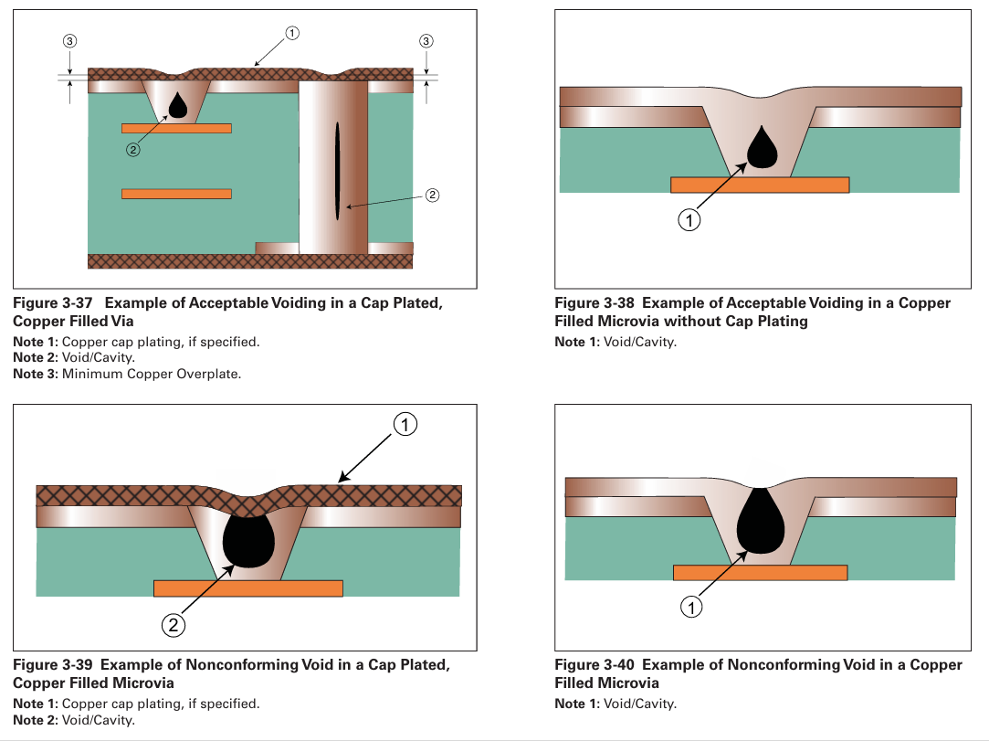
2. Incomplete Filling
Incomplete via filling happens when the filler does not fully occupy the via barrel. IPC-6012 does not directly specify fill rate, but in practical terms, Class 3 boards typically require ≥90% via fill, especially in via-in-pad configurations.
- Causes: Underdosed filler, poor alignment, rapid curing
- Consequences: Electrical discontinuity, weak solder joints
- Prevention: Proper volume control, optimized dispensing, degassing
In advanced HDI boards, even a 15% fill gap can impair signal transmission or cause surface depressions, which affect planarity during BGA soldering.
3. Cracks Under Thermal Stress
Cracking often develops when materials expand and contract at different rates. IPC-6012 Class 3 boards must withstand 6× thermal cycles between –55°C and +125°C without structural or electrical failure.
- Cause: CTE mismatch between filler and copper, rapid reflow ramp rates
- Impact: Intermittent signal loss, potential long-term circuit failure
- Testing: We run thermal cycling tests aligned with IPC-TM-650 2.6.7.2 guidelines to verify reliability
4. Delamination After Reflow
Delamination, a severe form of failure, involves separation between PCB layers, especially near filled vias. According to IPC-6012, delamination is unacceptable in Class 3 boards and must be prevented through proper lamination and moisture control.
- Triggers: Moisture absorption, rapid heating, epoxy expansion
- Typical scenario: After reflow or during high-temperature use
- Detection: Destructive cross-sectioning and C-SAM (scanning acoustic microscopy)
FAQs
1. What is the most common type of via fill in PCBs?
Non-conductive resin epoxy is the most widely used, especially for standard designs that don’t require thermal or electrical flow through the via.
2. When should conductive via filling be used?
When your design needs heat dissipation, power transfer, or high signal integrity, such as in RF or power boards.
3. Is via filling necessary for all PCBs?
No. It’s only needed when there’s a functional or layout reason, like vias under BGA pads or stacked via structures.
4. Can via fill improve thermal management?
Yes. Conductive via filling using copper or silver epoxy can transfer heat efficiently, helping prevent hotspots in high-power designs.
5. How do I know which via filling type is right for my project?
It depends on your board’s function. If you’re unsure, the engineering team at Best Technology will review your files and suggest the best option based on your goals.
You may also like


Tags: Difference between via filling and via plugging, via filling, Via filling in pcb, Via filling types