
What is a Black Pad in PCB?
A black pad in a PCB refers to a defect that occurs during the ENIG (Electroless Nickel Immersion Gold) surface finishing process. In the surface treatment process of ENIG, the radius of nickel atoms is smaller than that of gold atoms, so when gold atoms are arranged and deposited on the nickel layer, the surface grains will show a rough, loose and porous morphology, forming many voids. These gaps allow the bath to continue to react with the nickel atoms, causing them to oxidize. The undissolved nickel ions are trapped beneath the gold layer, forming nickel oxide, the so-called black pad.
When the black pad occurs, this area becomes brittle and doesn’t bond well during soldering. As a result, the connection between the component and the pad becomes unreliable.
Although it’s a well-known issue in the industry, many designers and engineers still face it during production. It’s not always visible during inspection, which makes it tricky. Once it affects the final board, the reliability drops—especially in fine-pitch components or BGA (Ball Grid Array) assemblies.
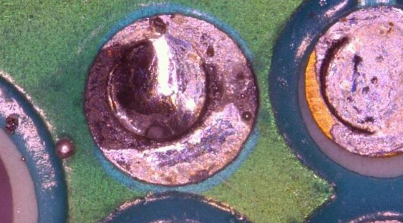
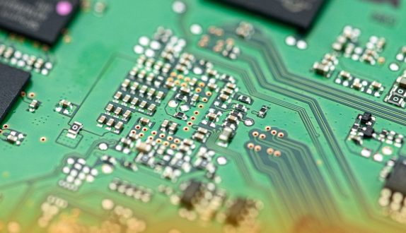
Black Pad Photos
A black pad appears as:
- Dark, muddy, or stained areas on the pad.
- Inconsistent finishes between pads.
- Rough texture or pits on the nickel layer.
- Exposed pads that don’t bond during reflow.
You can see the typical photos of black pad as following:
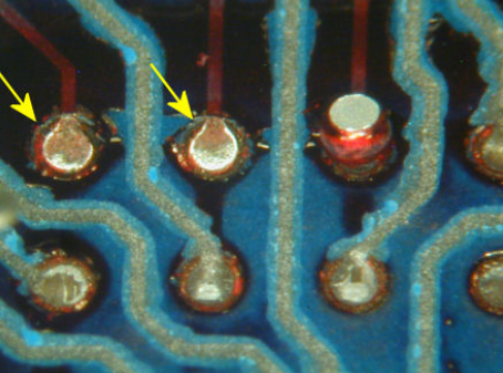
Engineers often spot it only after a failed solder joint. Sometimes, they notice it under a microscope after an assembly defect shows up. When looking at underfilled solder joints or cracks, a black pad might be the hidden culprit.
What Causes Black Pad Defects in ENIG Surface Finishes?
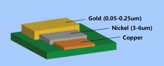
The main reason for the formation of black pads is that the nickel layer is eroded by excessive oxidation during ENIG surface treatment. There are two main steps in this process: a layer of nickel is deposited and a thin layer of gold is applied, as you can see in the ENIG structure diagram below.
Black pads caused by several factors, even when manufacturers strictly control chemical content, temperature, and raw materials, black pads sometimes occur. Here are some factors that Best Team faced during the PCB manufacturing:
1. High phosphorus content
Chemical nickel contains phosphorus. When the phosphorus content is too high, it diffuses into the nickel and causes nickel oxidation. A barrier is formed between gold and nickel during this process. It may cause reliable solder joints to delaminate and crack, resulting in electrical shorts in the PCB.
2. Corrosion during ENIG process
Gold plating is a necessary process for ENIG surface treatment commonly used in PCB manufacturing processes. If it is not operated properly, it will also lead to the formation of black pads. One of the reasons for the formation of black pads during gold deposition is the use of an aggressive gold bath. This nickel bath process causes rapid corrosion of nickel, resulting in black pads.
3. High gold content
High gold content can also lead to the formation of black pads. Excessive gold in the surface treatment of the nickel substrate can cause excessive galvanic corrosion and eventually form black pads.
4. Brittle fracture
Brittle fracture is a type of failure that occurs when a material is under high stress, but does not have the flexibility to withstand stress, and breaks suddenly without warning. This failure usually manifests as a black pad on the PCB surface. In addition, thermal stress, vibration, and shock can also cause brittle fracture. When this happens, it creates a crack structure within the nickel, causing an electrical short circuit.
In short, black pad is not a material defect—it’s a process problem. When ENIG isn’t done right, corrosion finds a way in.
How Can You Identify Black Pad on a PCB?
Spotting a black pad on a finished board is tough. It often hides beneath the surface and becomes visible only after soldering problems appear. But there are a few ways to detect it:
1. Visual Inspection
Do not inspect by your naked-eyes. Use a high-powered microscope to examine the pads instead. Look for dark spots, uneven textures, or dull finishes. These are the first signs.
2. X-Ray or Cross-Section
If you suspect the issue but can’t see it, advanced tools help. Cross-sectioning shows the damaged layers. X-ray inspection shows failed joints under BGAs and other tight packages.
3. Solder Joint Analysis
A cracked or non-wetting joint may indicate a black pad. If the solder ball peels off cleanly from the pad, you’re likely dealing with a surface that didn’t bond properly.
4. Pull or Shear Testing
This test measures joint strength. A weak joint may lead to a deeper look. If the break happens at the interface of the pad and solder, that’s a clue.
Although identification is possible, it’s much better to prevent the issue altogether. Because once it’s on the board, the damage is already done.
Why is Black Pad Considered a Serious Reliability Issue in PCBs?
Solder joints are the heart of any PCB. Every connection must be secure to handle temperature, vibration, and time. Black pad disrupts that by creating a brittle layer that doesn’t bond well with solder. And if black pads exist, here’s what defectives will happens:
- The solder joint may crack.
- Components may detach during vibration.
- Connections may fail over time due to thermal cycles.
- Weak pads may pass initial tests but fail later.
Even worse, most black pad defects don’t show up during inspection or basic testing. This delayed failure causes headaches in the field, leading to product returns, customer complaints, and loss of trust. That’s why manufacturers treat black pad as a critical issue. It’s not just cosmetic—it threatens the performance of the entire product.
How Does Nickel Corrosion Contribute to Black Pad in PCBs?
During the ENIG process, nickel is deposited first, followed by gold. The gold solution is slightly acidic. If the bath is too aggressive or the exposure is too long, it attacks the nickel. This chemical attack causes “spiky” corrosion. Think of it as tiny pits or cracks in the nickel. These spots are where the solder refuses to bond. Also, when the nickel has too much phosphorous, it becomes glassy and fragile. Under heat, the layer cracks more easily. This leads to more exposed areas and faster failure.
In short, nickel should form a smooth, strong base. But corrosion weakens it and opens the door to the black pad defect. The more pits and cracks it has, the worse the joint becomes.
How to Prevent Black Pads? – For Manufacturers
1. Improving ENIG process: By adjusting the formula of the gold plating solution and optimizing the parameter settings during the electroplating process, the erosion of the nickel layer can be effectively reduced.
2. Strengthening quality inspection: Strengthen quality control on the production line and conduct regular inspections to detect and correct the black pad phenomenon as early as possible.
3. Controlling the thickness of the gold layer: The thickness of the gold layer should not exceed 5 microns, and it is best to control it at around 3.2 to 3.6 microns to reduce excessive corrosion of the nickel layer.
4. Managing the temperature and concentration of the gold plating solution: Control the temperature and concentration of the gold water to avoid excessive temperature and too little gold to reduce excessive corrosion of the nickel layer and incomplete coverage of the gold layer.
5. Cleaning surface: After gold plating, high-temperature water flushing, pure water hot washing, ultrasonic or air blowing and other cleaning treatments are carried out to ensure the cleanliness of the welding surface.
How to Prevent Black Pads? – For Designers
1. Selecting alternative materials: For applications that require particularly high reliability, other types of surface treatment materials, such as silver or tin, can be considered, which may provide better performance.
2. Design considerations: Considering how to enhance the stability of the solder joints during the design stage, such as appropriately adjusting the position of the pads or increasing the number of solder joints, can help improve the overall reliability of the circuit board.
FAQs about Black Pads
1. Can black pad be repaired?
Unfortunately, no. Once a pad is affected, it must be scrapped. Rework doesn’t help because the damage lies beneath the surface.
2. Does black pad only affect by ENIG finishes?
Yes, it’s specific to ENIG. Other finishes like HASL, OSP, or ENEPIG don’t show this defect.
3. Is it common in high-volume production?
It depends on the manufacturer, looking for a reliable PCB manufacturer like Best Technology can reduce the black pad risks. With proper controls, it’s rare.
4. Does black pad affect all components equally?
Not always. Fine-pitch and BGA parts are more sensitive because they have small solder areas. Larger components may be less affected but still at risk.
You may also like


Tags: black pad, black pad pcb