Ceramic PCB is an innovation of traditional PCB circuit board. Ceramic PCB will use an organic compound called polyimide as solder paste, and ceramics (aluminum nitride, aluminum oxide, beryllium oxide) are often used as substrate materials. In the electronic power industry, ceramic PCB is a substitute for the traditional PCB technology based on FR-4 glass epoxy resin laminated with a thin copper layer.
The market of ceramic PCB is growing faster and faster because of its unique performance and cost-effectiveness. Compared with traditional FR4-PCB, they have many advantages, including thermal conductivity, chemical resistance, electrical insulation and high thermal shock resistance. So it is widely used in military, aerospace, consumer electronics industry and Internet of Things equipment.
What is a Ceramic PCB?
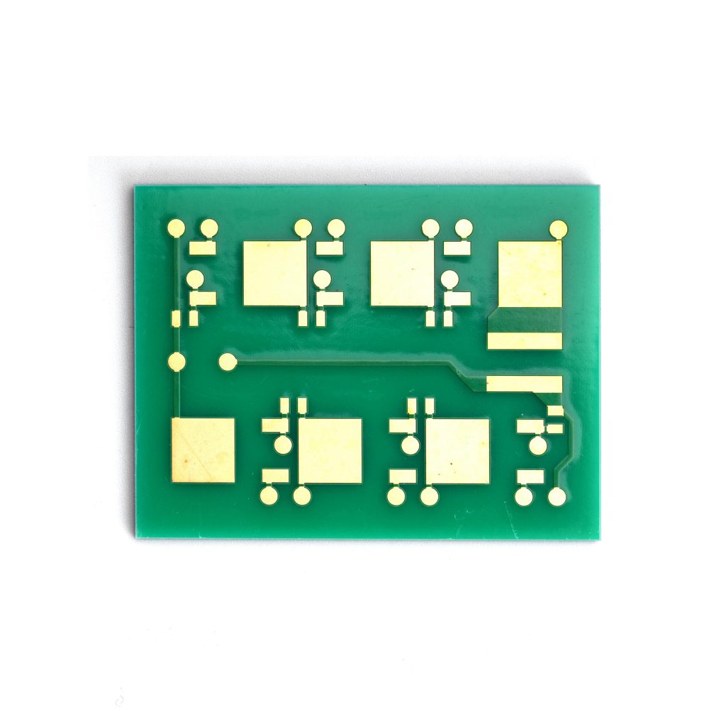
Ceramic PCB or ceramic circuit board is a kind of printed circuit board using ceramic material as substrate. Different from the traditional PCB which often uses FR4 and other materials, ceramic PCB has better heat dissipation and electrical insulation. These characteristics make ceramic PCB an ideal choice for high-power applications such as LED lighting, power electronics and automotive electronics.
Commonly used ceramic materials for ceramic PCB generally include alumina (Al2O3), aluminum nitride (AlN) and silicon carbide (SiC). These materials can provide the necessary thermal conductivity and mechanical strength for ceramic PCB applications, and ensure that the circuit board can withstand high temperature and harsh working conditions.
One of the main advantages of ceramic circuit boards is that they can handle higher power load without overheating risk, which significantly improves the service life of ceramic PCB. At the same time, the low coefficient of thermal expansion (CTE) in ceramic materials also reduces the risk of thermal stress and further improves the durability of ceramic PCB.
How to Make Ceramic PCB?
Due to the unique properties of ceramic materials, the process of manufacturing ceramic PCB is more complicated than traditional PCB. The manufacturing process usually involves several key steps:
Firstly, the first step is to select the appropriate ceramic materials according to the specific requirements of the circuit board.
The second step is to press and sinter the ceramic powder into the required shape and thickness after selecting the material. The sintering process involves heating the material to a high temperature to fuse the particles together, thus forming a dense and solid substrate.
The third step is to deposit a layer of metal (usually copper or gold) on the surface after the substrate is formed, then apply photoresist material to the metal layer, and use ultraviolet rays to expose the required circuit pattern, and then etch away the exposed area, leaving the circuit pattern.
Finally, after the circuit is formed, the circuit board should go through a finishing process to improve its performance and durability. Finally, the quality of the finished circuit board should be checked to ensure that it meets all the required specifications.
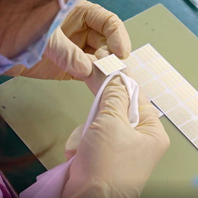
This process can make ceramic PCB highly reliable and can work normally under extreme conditions.
How Many Layers in Ceramic PCB?
Ceramic PCB can be made of multiple layers like traditional PCB, and its number of layers depends on the complexity of the circuit and the application requirements.
Single-layer ceramic PCB is composed of a single-layer ceramic material and a metal circuit at the top, which is usually used for heat dissipation applications.
Multilayer ceramic PCB is more complex, consisting of multilayer ceramic materials and metal circuits, which are stacked together and interconnected by vias. The extra layer allows more complex circuit design, enabling the circuit board to handle more signals and power for applications requiring higher functions.
The number of layers in ceramic PCB can range from one to several. Each additional layer will increase the complexity and cost of the circuit board, but it will also increase its function and performance, depending on its application scenario.
How Thick is Gold Conductor Printed on the Ceramic PCB?
The thickness of gold conductor on ceramic PCB is an important factor affecting the performance and durability of circuit board. The thickness of gold conductor depends on the application and required performance characteristics, and is usually in the range of 0.5 micron to 10 micron. Of course, a thicker gold layer can also be provided, which also brings better conductivity and more stable performance, especially in high-power applications, which also brings higher costs.
In high frequency applications, the thicker gold layer can reduce the signal loss, improve the overall performance of the circuit, and also better prevent wear and prolong the service life of PCB.
Considering the specific requirements of the application, the exact thickness of the gold conductor has been determined in the design stage. Our advanced manufacturing technology enables us to accurately control the thickness of the gold conductor and ensure that each circuit board meets the required specifications.
What is the Ceramic insulator on the Circuit Board Used For?
Ceramic insulators are generally used to electrically insulate different components and conductive paths on a circuit board, prevent short circuits and ensure that the circuit operates as expected. It plays a vital role in the performance and reliability of ceramic circuit boards.
Even a small amount of current leakage will cause serious problems. Ceramic materials of insulators provide excellent electrical insulation performance, which means that they can withstand high voltage without allowing current to pass through. In addition to electrical insulation, ceramic insulators also have thermal insulation properties, which can help control the heat generated by components on the circuit board.
Ceramic insulators are usually placed between metal conductors on the circuit board, which allows multiple conductive paths to be placed closely together without the risk of short circuit because they are electrically insulated from each other.
Generally speaking, ceramic insulator is a key component of ceramic PCB, which helps to improve its performance and reliability.
What equipment does BEST Technology have?
We use advanced machines at every step of the production process, from substrate molding to circuit molding and surface treatment, to ensure the highest quality ceramic PCB.
For substrate forming, we have high-precision press and sintering furnace, which can produce dense and uniform ceramic substrates.
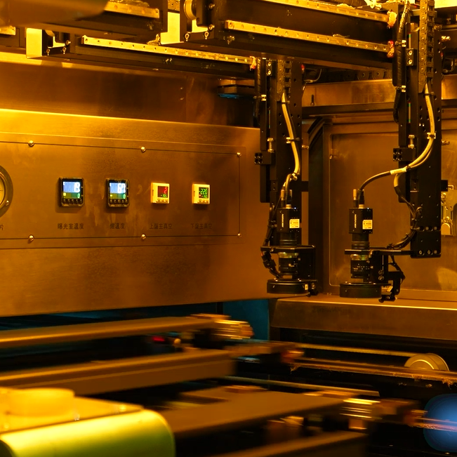
Our metallization process is also supported by advanced sputtering and chemical vapor deposition equipment to ensure that a consistent high-quality metal layer can be formed on the substrate.
At the same time, we also have cutting-edge lithography equipment for circuit formation, which enables us to create complex and accurate circuit patterns on the circuit board.
In addition to our advanced equipment, our team of technicians and engineers have rich experience in the production of ceramic printed circuit boards. Combined with our most advanced equipment, we can provide high-quality products that meet the most demanding requirements.
Ceramic PCB has a series of advantages, from materials to technology, each of which provides corresponding advantages, including excellent thermal management, electrical insulation and durability, making them an ideal choice for high power and high temperature applications. BEST Technology has advanced manufacturing technology, first-class equipment and commitment to quality, which can ensure that our ceramic PCB achieves the highest performance and the best quality. Whether you need a single-layer board or a complex multi-layer design, we have the expertise and equipment to provide products that meet your needs.


