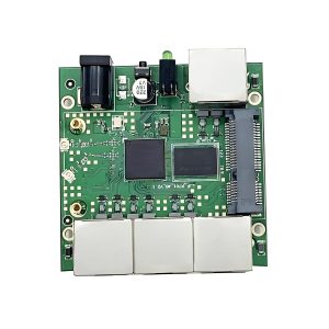
Generally speaking, the hole of PCB have PTH, blind via hole and buried hole.
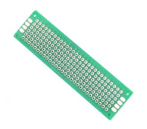
One of the most common is Plating Through Hole (PTH), the criteria of judging whether the hole is PTH, you can focus the PCB on the lamp, the light hole is PTH. During production, it can use the drill or laser to drilling the hole of PCB. So it is the most simple tpye of hole, and the cost are more cheaper than onters. But there also has some layer of PCB doesn’t need this hole, because it will take up some place of PCB.
The outermost layer of Blind Via Hole is connected to the adjacent inner’s plating hole, and the hole call “blind†since it can’t see the opposite. The production of blind hole is in order to make full use of space with the PCB circuit layers. This manufacture method should pay more attention to the depth(Z axis) of hole, almost no one in this way since the inner hole will be difficult to plate. And we can drill the hole of the connected circuit layer in advance when they in other layers and then stick up, but it needs precision positioning and contrapuntal device.
The internal layers’ connection but without conducting any circuit layer to the outer layer of PCB, which called the buried hole. This process cannot be completed by the way of stick up the drilling hole, it has to drill the hole in each layer. After bonding inner layer, it needs to plate firstly and then stick up all layers. Since it will spend more time to process than the PTH and Blind hole, so it will be more expensive. Finally, the production of buried hole just suitable for the HDI PCB, in order to enlarge the space of each layer for PCB.


