
Ball grid array (BGA) is a surface mount package for integrated circuits. Its ability to accommodate a large number of pins while maintaining a small footprint makes it ideal for modern electronic devices with limited space. BGA packages are used in a variety of applications, from consumer electronics such as smartphones and laptops to industrial equipment and automotive systems.
What is BGA?
Ball grid array (BGA) is a common surface mount package that is derived from pin grid array (PGA) technology. It uses a grid of solder balls or leads to conduct electrical signals from the integrated circuit board. Instead of using pins like PGA, BGA uses solder balls placed on a printed circuit board (PCB). By using conductive printed wires, PCBs support and connect electronic components.
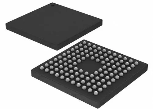
Unlike PGA, which has hundreds of pins and is difficult to solder, BGA solder balls can be evenly distributed without accidentally connecting them together. Solder balls are first placed in a grid pattern on the bottom of the package and then heated. By using surface tension when melting the solder balls, the package can be aligned with the circuit board. The solder balls cool and solidify, with accurate and consistent distances between each other.
What does a BGA do?
The main role of BGA (Ball Grid Array) packaging technology includes providing high-density, high-performance packaging solutions for microprocessors, ASICs, DSPs, PDAs, PLDs and other devices. This technology achieves surface mounting by making array solder balls on the bottom of the package substrate as the I/O end of the circuit to interconnect with the printed circuit board (PCB).
BGA packaging technology is small, light, and high-performance. It can provide more pins than other packaging technologies such as dual in-line package (DIP) or quad flat package (QFP). The entire bottom surface of the device can be used as pins instead of only the periphery.
This allows BGA packages to have shorter average wire lengths than periphery-limited package types, thereby providing better high-speed performance.
The advantages of BGA packaging are not only its high density and high performance, but also its less stringent requirements for welding accuracy. Even during the soldering reflow process, even if the solder ball is offset from the pad, the device position can be automatically corrected due to the surface tension of the solder.
What are the disadvantages of BGA?
The disadvantages of BGA packaging technology mainly include difficulty in detection, high difficulty in repair, relatively high production cost, stricter requirements on the reliability of solder joints, and sensitivity to temperature and humidity.
1. Difficulty in detection: Since the solder ball is located at the bottom of the chip, the traditional optical inspection method cannot effectively detect the welding quality, and X-ray detection and other equipment must be used, which increases the cost and time of detection.
2. High difficulty in repair: If there is a welding problem, the BGA packaged device needs to be disassembled and reassembled. This process has high technical requirements and certain risks.
3. Relatively high production cost: Compared with QFP packaging, BGA packaging has higher material, production and inspection costs.
4. More stringent requirements on the reliability of solder joints: Due to its small size, the BGA packaging method has very high requirements on solder joints. If there are problems such as empty solder joints and cold solder joints in the solder joints, the BGA package will fail.
5. Sensitive to temperature and humidity: BGA packaged components are very sensitive to temperature and humidity and need to be stored under constant temperature and dry conditions.
These shortcomings have limited the widespread application of BGA packaging technology to a certain extent, especially in application scenarios with high requirements for cost, reliability and environmental adaptability.
How is BGA made?
The production process of BGA (ball grid array package) mainly includes several key steps, which ensure the high quality and high reliability of BGA package.
1. Wire bonding PBGA packaging process flow:
Substrate preparation: extremely thin copper foil is laminated on both sides of the BT resin/glass core board, and then drilling and through-hole metallization are performed.
Graphic production: Use conventional PCB processing technology to make graphics on both sides of the substrate.
Solder mask production: Add solder mask and make graphics to expose electrodes and welding areas to improve production efficiency. A substrate usually contains multiple PBGA substrates.
2. BGA area via plugging:
The vias in the BGA pad area generally need to be plugged to prevent foreign matter in the hole or to protect the service life of the via, and to prevent the via from tinning during the reflow soldering of the SMT patch, causing a short circuit on the other side.
3. Via in the plate, HDI design:
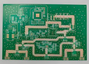
For BGA chips with small pin spacing, when the pin pad cannot be connected due to the process, it is recommended to directly design the via in the plate, and use the HDI blind buried hole wiring method to design the PCB, punch the via in the plate on the BGA pad, punch the buried hole in the inner layer, and conduct the wiring in the inner layer.
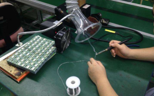
4. BGA welding process:
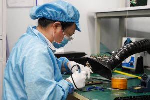
Printing solder paste: Apply an appropriate amount of solder paste evenly on the PCB pad to ensure that the patch components and the corresponding pads on the PCB achieve good electrical connection and sufficient mechanical strength during reflow soldering.
Device placement: Use a placement machine to accurately mount the chip components to the corresponding position on the PCB surface printed with solder paste or patch glue.
5. Special size design and automated production:
BGA features include high pinhole density, easy automated production, high reliability, and the ability to design special sizes to achieve a more compact chip layout.
What is the difference between PCB and BGA?
The main differences between PCB and BGA are their structure, function, and application scenarios.
1. Structure:
PCB (printed circuit board) is a basic electronic component that provides an electrical connection path between components. BGA (ball grid array package) is an advanced packaging method that connects components to PCB through a spherical pad array, with the advantages of high density and high reliability.
The pins of BGA are spherical and are generally directly soldered on the PCB board. Desoldering requires a special BGA rework station, and individuals cannot desolder; while the pins of PGA (pin grid array package) are pin-shaped. When installing, the PGA can be inserted into a special PGA socket for easy disassembly.
2. Functions and application scenarios:
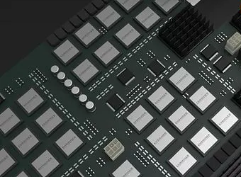
BGA packaging effectively uses PCB space, which helps save enough space for customization in PCB and improve its efficacy. The size of BGA package is very small, so these PCBs have less heat dissipation and are easy to achieve the dissipation process.
There are no bendable or fragile pins in BGA package, so the durability of these PCBs is increased, and good electrical performance is also ensured. The pads of BGA package are large enough to make it easy to solder and easy to operate, so easy soldering and handling make it very fast to manufacture.
In summary, BGA, as an advanced packaging technology, has been widely used in high-performance electronic products through its unique ball grid array structure and high density and high reliability characteristics. Traditional PCBs provide basic electrical connection paths and are the basic components of electronic devices.
How many types of BGA are there?
There are many types of BGA, mainly including:
1. PBGA (plastic package BGA): This is the most commonly used BGA packaging form, made of plastic materials and plastic processes.

2. CBGA (ceramic BGA): This packaging type uses a multi-layer substrate with precious metal interconnect circuits.
3. CCGA (ceramic solder column array)
4. TBGA (BGA with tape)
5. MBGA (metal BGA)
6. FCBGA (flip chip BGA)
7. EBGA (BGA with heat sink)
In addition, BGA can be divided into staggered type, full array type, and peripheral type according to the arrangement of solder balls.
Conclusion:
Ball grid array (BGA) packaging is a key technology in modern electronic products. It makes it possible to develop more powerful and compact devices. BGA has become the first choice for applications that require high performance, reliability and miniaturization.
BGA packaging is famous for its advanced packaging technology. BEST Technology is recognized as the most trusted one-stop electronic circuit solution provider in the world, and BGA production is one of its most important projects. We specialize in the production and assembly of PCBs containing BGA packaging.
You may also like


Tags: BGA