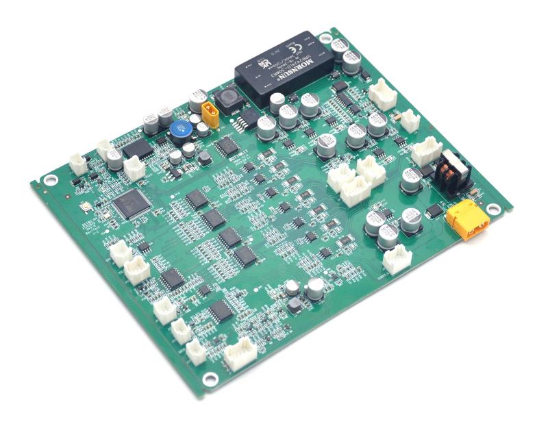
Surface Mount Technology (SMT) has revolutionized electronics manufacturing, allowing for compact, efficient, and high-speed production of printed circuit boards (PCBs).
But designing an effective PCB requires an understanding of critical clearance rules, especially when dealing with SMT components. Proper body-to-body clearance can influence reliability, manufacturability, and long-term performance.
What Is the Clearance Rule for PCB?
PCB design follows strict clearance rules to ensure that components work as expected. Clearance refers to the minimum space required between elements on the board to prevent interference, short circuits, or damage during soldering and operation.
The general clearance rules for PCBs depend on factors such as voltage, current, and operational environment. For standard PCBs, a common clearance rule is 0.1 mm to 0.2 mm between components, though this can vary based on specific needs. It’s essential to consult design guidelines from the PCB manufacturer, as they may provide specific instructions based on their capabilities.
How Close Can Components Be on a PCB?
Component spacing is one of the most crucial elements in PCB design. The minimum distance between SMT parts, or body-to-body clearance, is influenced by several factors, including component size, heat dissipation, and soldering methods.
For standard designs, a minimum body-to-body clearance of 0.2 mm to 0.5 mm is typical for most SMT components. This spacing ensures proper airflow, heat dissipation, and avoids accidental shorts during soldering. Smaller devices may require tighter clearances, but you should always account for potential manufacturing limitations and performance requirements.
Maintaining adequate clearance also helps with inspection and rework. If components are too close together, it becomes challenging to check for soldering defects or make repairs, increasing costs and time for revisions.
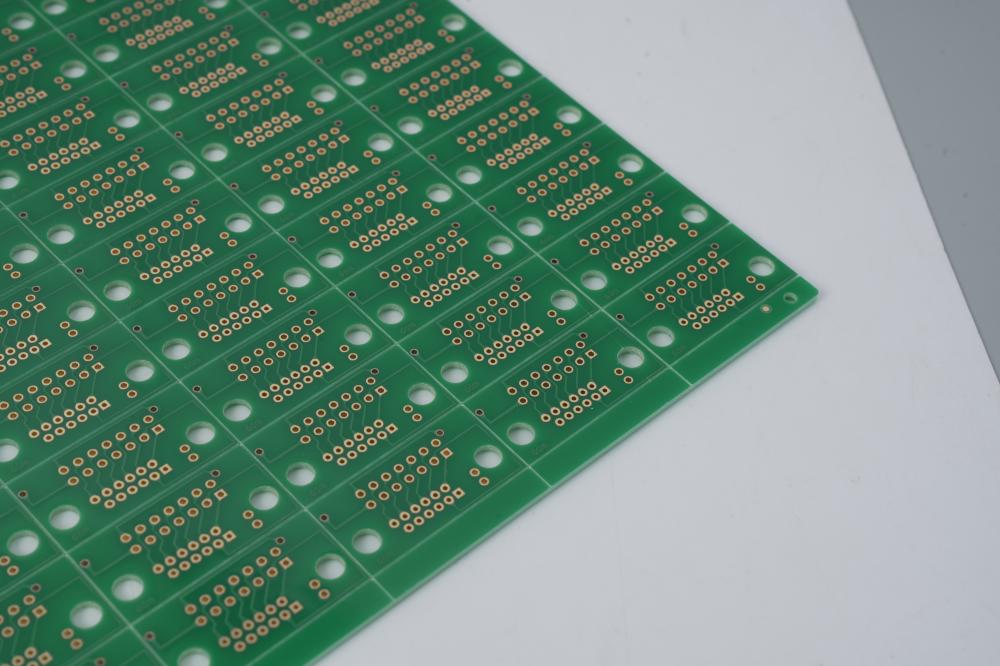
What Is the Spacing Between SMD Pads?
Surface Mount Devices (SMD) pads are small metal areas on the PCB where components are soldered. The pad spacing plays a critical role in ensuring good electrical contact while avoiding issues like bridging, where solder connects unintended pads, causing shorts.
The spacing between SMD pads is often defined by the component’s package type.
For example:
– For a 0603 package, the typical pad spacing might be around 0.8 mm.
– For a larger 1206 package, it could be around 1.5 mm or more.
In addition to pad spacing, the size of the pad must be carefully chosen to ensure that it supports the component correctly without causing issues during soldering. If the pads are too close, there is a higher chance of bridging, especially when using automated processes like reflow soldering. On the other hand, too much spacing could lead to poor contact, reducing the reliability of the connection.
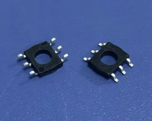
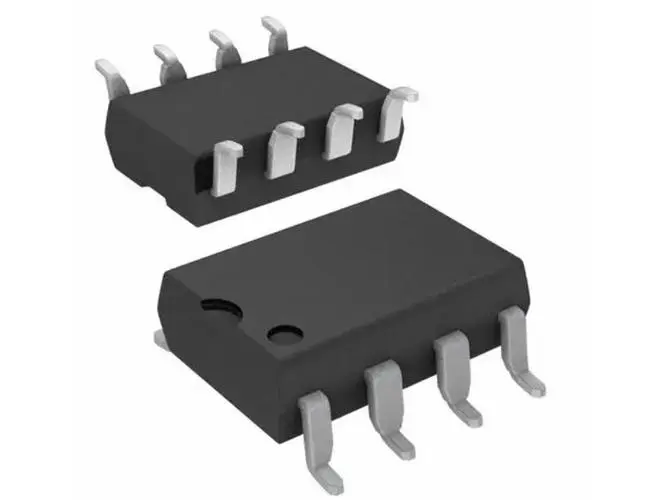
What Is the Difference Between SMT and SMD Components?
SMT (Surface Mount Technology) refers to the process of mounting components directly onto the surface of a PCB. SMD (Surface Mount Device) is the term for the components themselves.
In essence:
SMT: The technology and process of assembling components on a PCB.
SMD: The individual components that are placed using SMT techniques.
The two terms are often used interchangeably, but it’s helpful to remember that SMT refers to the process, while SMD refers to the devices used in that process.
SMT has advantages over older methods like through-hole mounting, including reduced size and weight, faster production, and the ability to place components on both sides of the PCB. SMD components are designed specifically to benefit from these advantages, often smaller and lighter than their through-hole counterparts.
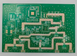
How Close Can PCB Traces Be?
PCB traces are the conductive pathways that connect components on the board. Proper spacing between these traces is critical to avoid electrical interference, arcing, or short circuits.
The minimum trace clearance depends on the operating voltage and current. For low-voltage circuits, traces can be closer together, but higher-voltage designs require more significant separation to avoid electrical breakdown.
For example:
– For a PCB operating at less than 100V, a typical trace clearance might be around 0.2 mm to 0.5 mm.
– For high-voltage designs (e.g., 600V), trace spacing might need to increase to 3 mm or more.
It’s essential to follow the manufacturer’s recommendations and industry standards like IPC-2221 when determining trace clearance. Additionally, wider spacing can improve performance, particularly in high-frequency circuits where issues like crosstalk become more prominent.
What Is the Edge Clearance of a PCB?
Edge clearance refers to the distance between components or traces and the outer edges of the PCB. Ensuring adequate clearance near the edges prevents damage during manufacturing and assembly. It also allows room for board routing, where mechanical tooling may cut the board from a larger panel.
The general rule for edge clearance is to keep components at least 1 mm to 2 mm away from the PCB’s edge. This gives enough room for mechanical handling, ensures that traces aren’t damaged during cutting, and reduces the risk of short circuits due to edge contact.
In designs that incorporate connectors or other mechanical features near the board’s edge, additional clearance may be necessary to accommodate mounting holes or alignment features.
Additional Considerations for SMT Clearance and Spacing
In addition to the factors already covered, there are several other considerations when designing SMT PCBs:
- 1. Thermal Considerations: Proper body-to-body clearance helps ensure that heat can dissipate effectively. Crowding components too closely together can lead to hot spots, reducing the life of the board and its components.
- 2. Automated Assembly: If you’re using automated pick-and-place machines for assembly, sufficient clearance is needed for accurate placement. Overly tight layouts can lead to assembly errors or slower production times.
- 3. Manufacturability: PCB fabricators have limitations on how closely they can place components, traces, and vias. These limitations vary from one manufacturer to another, so it’s essential to consult with them early in the design process to avoid issues during production.
- 4. Inspection and Rework: Allowing enough space between components simplifies inspection and rework. If something goes wrong during assembly, having accessible components makes repairs quicker and more cost-effective.
Practical Tips for Ensuring Proper Clearance Between PCBs
- Use Design Guidelines: Always reference your PCB manufacturer’s design rules. These will give you specific guidance on spacing, trace widths, and clearances based on their capabilities.
- Optimize Component Placement: Group similar components together when possible. For instance, resistors and capacitors can often be placed closer together than components that require heat dissipation.
- Account for Heat Dissipation: Keep heat-generating components like power ICs and transformers farther apart from sensitive components like sensors. This minimizes heat transfer and reduces the chance of thermal stress.
- Perform Electrical Testing: Simulate your design using PCB software to check for potential clearance violations, especially around high-voltage areas and traces that could experience crosstalk.
- Test with Prototypes: Before full production, build a prototype to test clearance in real-world conditions. This will allow you to identify any spacing issues and resolve them before scaling production.
Conclusion:
Achieving proper body-to-body clearance for SMT parts is critical for the performance and longevity of your PCB. By following the established guidelines for component spacing, pad placement, trace clearance, and edge spacing, you can ensure that your design meets both functional and manufacturability requirements. This not only improves the reliability of your board but also reduces the likelihood of costly errors during assembly and operation.
Invest time in careful planning during the design phase to avoid unnecessary revisions later on. Working closely with your PCB manufacturer and utilizing design simulation tools can go a long way in ensuring your final product performs as expected.
In the end, understanding and applying the right clearance rules will result in a robust, reliable, and efficient PCB design that meets the demands of modern electronics.