
In this field full of innovation and challenges, ceramic base pcb have quietly emerged and quickly attracted the attention of the industry with their excellent performance and broad application prospects.
What is a ceramic base pcb?
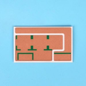
Ceramic base pcb are made of ceramic as the matrix material through complex and sophisticated processes. This type of circuit board has many unique properties, which makes it widely used in many fields.
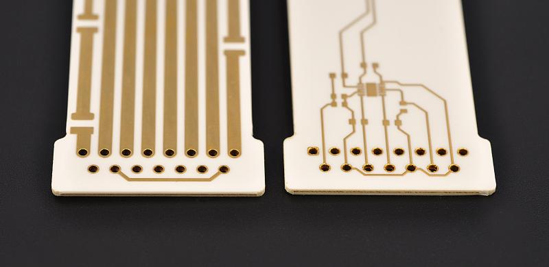
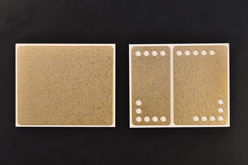
Ceramic substrates are easier to break than glass fiber boards, and the process is more difficult than ordinary PCB boards, and the process technology requirements are high. In the production process, there are important process links such as drilling, copper coating, and etching.
The copper coating process plays a key role in the ceramic substrate PCB process. The commonly used copper coating processes are DBC process and DPC process. In the DPC process, the electroplating process is adopted, and the adhesion layer and seed layer are formed on the ceramic surface through the sputtering process to increase the adhesion strength of the metal circuit and play a conductive role.
The etching of ceramic-based circuit boards is divided into inner layer etching and outer layer etching. Different etching methods have different processes and characteristics. At the same time, some problems may occur in the etching process, such as incomplete film removal, board surface oxidation, incomplete copper etching, excessive copper etching, etc., and corresponding improvement methods need to be adopted.
In short, ceramic base pcb occupy an important position in the electronics field due to their unique properties and complex manufacturing processes.
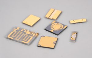
What are the different types of ceramic PCB?
(I) Classification by material
- Alumina ceramic substrates are the most commonly used substrate materials in the electronics industry. They have high strength and chemical stability, rich raw material sources, and are suitable for various technical manufacturing and different shapes.
- Beryllium oxide ceramic substrates have a higher thermal conductivity than metal aluminum and are used in situations where high thermal conductivity is required, but the temperature drops rapidly after exceeding 300°C, and their toxicity limits their own development.
- Aluminum nitride ceramic substrates have high thermal conductivity and expansion coefficients that match Si, and are ideal large-scale integrated circuit heat dissipation substrates and packaging materials.
- Silicon nitride ceramic substrates have higher mechanical strength than other ceramics and can achieve long life in harsh working environments and HEV/EV and other renewable energy application conditions.
(II) Classification by process
- Thick film ceramic PCBs use screen printing technology to coat metal slurry on the surface of ceramic substrates, which are dried and sintered at high temperature. Its advantage is that the process is relatively simple and the cost is low.
- Low-temperature co-fired ceramic (LTCC) PCB first mixes inorganic alumina powder with about 30% – 50% glass material and organic binder to make a slurry, scrapes it into sheets to form a green embryo, then drills through holes according to the design of each layer, uses screen printing technology to fill holes and print circuits, and finally sintered at 850 – 900℃.
- High-temperature co-fired ceramic (HTCC) PCB first adds ceramic powder to an organic binder to make a paste slurry, scrapes it into sheets to form a green embryo, then drills through holes, uses screen printing technology to fill holes and print circuits, and sintered at 1300 – 1600℃.
What are the characteristics of ceramic base pcb?
(I) Performance advantages
- First, it has strong mechanical stress, can maintain a stable shape in various complex use environments, and is not easily deformed by external forces.
- High thermal conductivity is one of its notable features. For example, the thermal conductivity of alumina ceramic substrates is between 28 and 35 W/(m・K), and the theoretical thermal conductivity of aluminum nitride ceramic substrates at room temperature is 319W/(m・K), which allows the heat generated by electronic components to be quickly dissipated, effectively avoiding circuit failures caused by local overheating.
- High insulation ensures the safe and stable operation of the circuit and prevents leakage. Good thermal cycle performance is also one of its advantages, with a cycle number of up to 50,000 times and high reliability.
- In an environment with extreme temperature changes, ceramic base pcb can still maintain stable performance, which is crucial for some electronic devices that need to work in harsh environments.
(II) Comparison with traditional PCBs
Compared with conventional PCBs, ceramic base pcb have obvious advantages.
- In terms of thermal conductivity, traditional PCBs usually require heat dissipation holes, inner metal planes, heat dissipation platforms, and active cooling devices such as fans to remove heat from hot components. However, ceramic base pcb, with their high thermal conductivity, do not require these additional components and can easily transfer heat to active cooling components, thermal landings, or device packaging.
- In terms of mechanical strength, ceramic base pcb have higher compressive strength and surface hardness, higher durability, and longer service life.
- In terms of corrosion resistance, ceramic materials are extremely resistant to most chemicals and are suitable for applications in harsh environments.
However, ceramic base pcb also have some disadvantages.
- The cost is higher than that of standard PCBs, which is due to the relatively complex materials and manufacturing processes.
- Reduced availability, because the current production scale of ceramic base pcb is relatively small and the manufacturing difficulty is relatively high.
- Fragility is one of the main disadvantages of ceramic base pcb, and currently only small-area circuit boards can be manufactured.
Manufacturing process of ceramic base pcb
(I) Drilling process
Ceramic substrates are generally drilled by laser. Laser drilling technology has many advantages over traditional drilling technology, such as high precision, high surface flatness, roughness of 0.1μm~0.3μm, laser drilling aperture of 0.15mm-0.5mm, and even below 0.06mm.
(II) Copper coating process
Commonly used copper coating processes include DBC process and DPC process.
In the DPC process, electroplating process is adopted. Copper coating refers to covering the area without wiring on the circuit board with copper foil, which is connected to the ground wire to increase the ground wire area, reduce the loop area, reduce the voltage drop, and improve the power supply efficiency and anti-interference ability.
In addition to reducing the ground wire impedance, copper coating also has the functions of reducing the loop cross-sectional area and enhancing the signal mirror loop.
Therefore, the copper coating process plays a very critical role in the ceramic substrate PCB process. Incomplete, truncated mirror loop or incorrectly positioned copper layer often leads to new interference, which has a negative impact on the use of the circuit board.
(III) Etching process
The etching of ceramic substrates is divided into inner layer etching and outer layer etching. The inner layer etching adopts acid etching, and wet film or dry film is used as resist; the outer layer etching adopts alkaline etching, and tin-lead is used as resist.
1. The alkaline etching process is as follows:
- Defilming: Use film stripping liquid to remove the film on the circuit board surface to expose the unprocessed copper surface.
- Etching: Use etching liquid to etch away the unnecessary bottom copper, leaving a thickened circuit.
- New washing liquid: Use monohydrated ammonia without copper ions, and use ammonium chloride solution to remove the residual liquid on the board surface.
- Hole filling: Mainly remove excess palladium ions in non-plated through holes to prevent gold ions from being deposited in the gold immersion process.
- Tin stripping: Use nitric acid solution to strip the tin-lead layer.
2. Acid copper chloride etching process:
- Development: Use sodium carbonate to dissolve the part of the dry film that has not been irradiated by ultraviolet light, and retain the part that has been irradiated.
- Etching: According to a certain proportion of solution, the copper surface exposed to the outside after the dry film or wet film is dissolved is dissolved with acidic copper chloride etching solution.
- Film stripping: According to a certain proportion of solution, the protective film on the circuit is dissolved under a specific temperature and speed environment.
Common problems and improvement methods of etching process:
- 1. Incomplete film stripping: It may be that the film stripping solution concentration is not enough or the operation time is insufficient. It is necessary to adjust the film stripping solution concentration or extend the operation time.
- 2. Board surface oxidation: It may be that the exposure time is too long or the ambient humidity is high during the etching process. The exposure time should be shortened as much as possible and the ambient humidity should be controlled.
- 3. Incomplete copper etching: It may be that the etching solution concentration is low or the etching time is short. The etching solution concentration needs to be increased or the etching time needs to be extended.
- 4. Excessive copper etching: It may be that the etching time is too long or the etching solution concentration is too high. The etching time should be reduced or the etching solution concentration should be reduced.
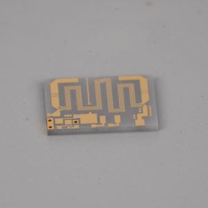
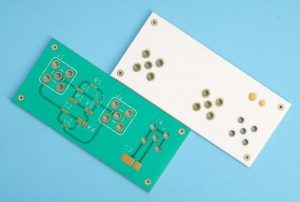
What is a ceramic PCB used for?
(I) High-frequency applications
Ceramic base pcb perform well in high-frequency applications. Due to its high dielectric constant and low dielectric loss tangent value, it can maintain good stability and reliability in high-frequency signal transmission.
In high-frequency electronic equipment such as mobile phones, microwave ovens, radars, communication equipment and other fields, ceramic base pcb can effectively reduce noise interference and improve signal transmission quality. In addition, ceramic base pcb can withstand higher output power to meet the power requirements of high-frequency equipment.
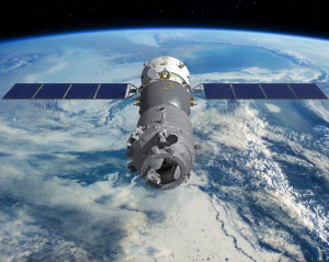
(II) Aerospace
ceramic base pcb have important application value in the aerospace field. Its thermal expansion coefficient is very close to silicon and much lower than most common metals, which enables it to work well with other electronic components in an environment with extreme temperature changes and will not damage the chip due to thermal expansion and contraction.
In key parts of aircraft electronic equipment, navigation systems, rocket engines, etc., ceramic base pcb can withstand harsh environments such as high temperature, high pressure, radiation, and corrosion to ensure the reliability of the equipment.
(III) Other fields
ceramic base pcb are also widely used in power devices, communication substrates, mobile phone application module substrates, automotive electronic substrates and other fields.
In the field of power devices, such as the power electronic system of electric vehicles, DPC ceramic circuit boards, as ideal electronic substrates, play an important role in battery management systems, motor drive systems and fast charging systems.
In terms of communication substrates, ceramic substrates, that is, high-frequency filters used in high-frequency ceramic substrates, are used in 5G network equipment. They have low high-frequency loss and low dielectric constant. The dielectric loss of signals propagating in them can reach the lowest among all current PCBs, which is particularly suitable for high-frequency communications such as 5G.
In the mobile phone application module substrate, ceramic base pcb can meet the requirements of mobile phones for miniaturization and high performance. In the field of automotive electronic substrates, new energy vehicles have high requirements for heat dissipation. Ceramic substrates have good heat dissipation effects and can dissipate high heat in the power system in time to ensure the normal operation of large power loads.
Development prospects of ceramic base pcb
(I) Market size growth
In recent years, the market size of ceramic base pcb has shown a trend of continuous growth.
First, with the development of miniaturization, high performance and multi-functionality of electronic equipment, the requirements for heat dissipation performance, insulation performance and high-frequency characteristics of circuit boards are getting higher and higher.
Secondly, technological progress has driven the cost reduction and production efficiency improvement of ceramic base pcb, which will further promote the expansion of its market size.
Finally, the continuous emergence of emerging application fields has also brought a broad market space for ceramic base pcb.
(II) Industry challenges and opportunities
Technical barriers: The ceramic base pcb industry is a technology-intensive industry. Its research and development and production require knowledge of multiple disciplines such as electronics, computers, materials, and chemicals, and there are many product types, long processes, and complex process technologies.
Fundamental barriers: The ceramic base pcb industry has complex process technologies, many links, and high customization requirements. In the early stage, a large amount of capital investment is required for the purchase of equipment, new plant buildings and supporting facilities, procurement of raw materials, and the employment of R&D and production personnel.
Talent barriers: The ceramic circuit board industry is highly professional. Technical and R&D personnel not only need to have professional knowledge in multiple fields, but also need to have a deep understanding and familiarity with product applications, process flows, equipment improvements, etc.
In summary, although the ceramic base pcb industry faces many challenges, it has also ushered in rare development opportunities. Driven by policy support, market demand growth, and technological innovation, the ceramic base pcb industry is expected to achieve sustained and rapid development.
You may also like


Tags: ceramic PCB, PCB, PCBA