
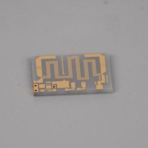
In this ever-changing era, electronic devices are changing our lives at an unprecedented speed. From smartphones to cars to industrial automation equipment, these products all hide an important component – ceramic printed circuit boards (Ceramic PCBs).
What are the commonly used materials for ceramic PCB substrates?
Imagine that in a tiny space, there are countless electronic components, which are closely arranged and interconnected to form a complex and sophisticated network. This is the working environment of ceramic PCBs. In order to ensure that these components can work normally under harsh conditions such as high temperature and high pressure, it is crucial to choose a suitable substrate.
Commonly used ceramic PCB substrates are mainly the following:
1. Alumina (Al2O3):
- It is one of the preferred materials for its excellent insulation performance, good thermal conductivity and high mechanical strength.

- Alumina substrates are usually used to make single-layer ceramic PCBs, which are suitable for applications under medium temperature and pressure conditions.
- It has extremely high chemical stability and is not easy to react with other substances, thus ensuring the long-term reliability of the circuit.
2. Aluminum nitride (AlN):
- Compared with aluminum oxide, aluminum nitride has higher thermal conductivity and can dissipate heat more effectively, making it an ideal choice for manufacturing high-performance electronic products.

- Aluminum nitride substrates are often used to make double-layer or multi-layer ceramic PCBs, especially for high-frequency signal transmission and high power density applications.
- In fields such as semiconductor packaging and LED lighting, the outstanding performance of aluminum nitride makes it one of the indispensable materials.
3. Silicon nitride (Si3N4):
- It is known for its excellent heat resistance and chemical stability, and it still performs well in extreme environments.
- Silicon nitride substrates not only have extremely high mechanical strength, but also can withstand a higher temperature range. They are widely used in demanding scenarios such as aerospace, automotive electronics and military equipment.
What are the commonly used conductor materials for ceramic PCBs?
Conductor materials play an extremely important role in ceramic PCBs. They are responsible for transmitting signals and electricity and are the link between various functional modules.
Common conductor materials include precious metals such as copper, gold, and silver, as well as nickel plating. Among them, copper is widely used for its good conductivity and affordable price; gold shines in high-end applications for its excellent corrosion resistance; silver is between the two, combining cost-effectiveness and reliability.
- As the most commonly used conductor material, copper foil is soft enough to easily combine with ceramic substrates to form a durable circuit path.
- Gold foil is mainly used in occasions that require high reliability and long life, such as aerospace, medical equipment, etc. The oxidation resistance and corrosion resistance of gold enable it to maintain stable electrical performance in extreme environments, ensuring the normal operation of key components.
- Silver foil is widely used in mid- and low-end products due to its good conductivity and low cost. Silver’s conductivity is second only to gold, but it is more affordable in terms of cost and is suitable for large-scale production and application. In certain specific fields, such as high-frequency circuits and wireless communication equipment, silver foil can also play an important role.
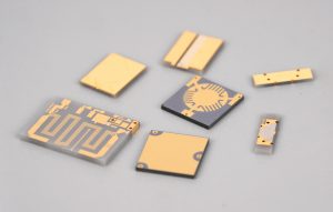
What are the types of ceramic PCBs?
With the advancement of technology, ceramic PCBs have also developed into various types to adapt to various application scenarios:
1. Single-layer ceramic PCB:
- Simple structure, low cost, suitable for occasions with low performance requirements.
- This type of PCB usually has only one layer of ceramic substrate, on which a layer of conductor material is laid to form a basic circuit layout.
- Single-layer ceramic PCBs are mainly used for entry-level electronic products, such as ordinary household appliances and basic communication equipment.
2. Double-layer or multi-layer ceramic PCB:
- By stacking multiple layers of ceramic substrates and setting interconnection channels between them, more complex circuit designs can be achieved, which is suitable for high-end products that require high-density integration.

- This type of PCB can accommodate more electronic components and more complex circuit structures, and is widely used in high-performance computing, advanced medical equipment and high-end automotive electronic systems.
- Multilayer ceramic PCBs have high design flexibility and can be customized according to specific needs to achieve optimal performance.
3. Hybrid ceramic PCB:
- Combining ceramic substrates of different materials, giving full play to their respective advantages, suitable for use in special environments.
- This type of PCB usually uses two or more ceramic materials, such as a combination of alumina and aluminum nitride, which can ensure good thermal conductivity and provide sufficient mechanical strength.
- Hybrid ceramic PCBs are suitable for applications with extreme temperature changes and high pressure conditions, such as deep-sea exploration equipment and space exploration instruments.
Advantages and characteristics of ceramic PCB
The reason why ceramic PCBs stand out among many materials is inseparable from their unique advantages:
High temperature resistance:
- It can remain stable at temperatures up to 1000℃, making it an ideal choice for high-temperature working environments.
- Ceramic materials themselves have extremely high melting points and are not easy to deform or damage even under extremely high temperature conditions, which enables ceramic PCBs to operate reliably in extreme environments.
High reliability:
- It will not deform or damage even under long-term exposure to extreme conditions, ensuring the continuous and reliable operation of the system.
- Ceramic materials have high chemical stability and are not easy to react with other substances, so they can maintain stable electrical performance in harsh environments.
Excellent thermal management capabilities:
- Efficient heat dissipation helps to extend the life of components and improve overall efficiency.
- The high thermal conductivity of ceramic materials enables it to quickly conduct heat away, effectively reducing the temperature of the circuit board, thereby improving the reliability and service life of the system.
Environmentally friendly and pollution-free:
- The production process meets green environmental protection standards and is easy to recycle and reuse after disposal.
- The production process of ceramic PCBs produces less waste, and the discarded materials can be recycled, which is in line with the concept of sustainable development.
These characteristics make ceramic PCBs an important force in promoting scientific and technological progress, and continue to lead the industry to a higher level.
What are the applications of ceramic PCBs?
From aerospace to medical equipment, from automotive electronics to communication facilities, ceramic PCBs are everywhere.
In satellite navigation systems, ceramic PCBs ensure positioning accuracy with their reliable signal transmission capabilities; in medical devices such as pacemakers, they rely on their ability to accurately control current to protect patient safety. In addition, in the construction of 5G base stations, ceramic PCBs also play an irreplaceable role, supporting the demand for high-speed data transmission.
Specific application cases are as follows:
- 1. Aerospace: In satellite communication systems, the high reliability of ceramic PCBs ensures the accuracy of data transmission. During long-term flight, ceramic PCBs can resist extreme temperature changes, maintain stable electrical performance, and ensure unimpeded communication between satellites and ground stations.
- 2. Medical equipment: In implantable medical devices such as pacemakers, the miniaturization and high reliability of ceramic PCBs become key factors. Ceramic materials have good biocompatibility and will not have adverse effects on human tissues. At the same time, they can provide precise current control to ensure therapeutic effects.
- 3. Automotive electronics: In modern automobiles, ceramic PCBs are widely used in key components such as engine control systems, sensors, and navigation systems. The high temperature resistance of ceramic PCBs enables it to operate reliably in high-temperature environments in the engine compartment, ensuring the safety and comfort of the vehicle.
- 4. 5G communication: In the construction and maintenance of 5G base stations, the efficient heat dissipation capacity and high-density integration characteristics of ceramic PCBs make them an ideal choice. Ceramic PCBs can handle a large number of data transmission tasks and ensure the high-speed and stable operation of 5G networks.
What is the production process of ceramic PCB?
The production process of ceramic PCBs is very delicate, and every step needs to be strictly controlled to ensure the high quality of the final product.
- 1. Raw material preparation: First, the required ceramic powder and other raw materials need to be prepared to ensure their purity and uniformity.
- 2. Molding: The ceramic powder is made into a substrate by pressing or casting. The temperature and pressure need to be strictly controlled during the molding process to ensure the flatness and consistency of the substrate.
- 3. Sintering: The formed substrate is placed in a high-temperature furnace for sintering. The sintering process requires precise control of the temperature curve to ensure the density and stability of the ceramic substrate.
- 4. Metallization: A layer of conductor material such as copper, gold or silver is applied to the ceramic substrate by electroplating, spraying or other means. This process requires highly precise operation to ensure the uniform distribution and good adhesion of the conductor layer.
- 5. Circuit design and etching: According to the circuit design drawings, etching is performed on the conductor layer to form the required circuit pattern. The etching process requires the use of special chemicals, and the time and temperature need to be precisely controlled to ensure the accuracy and clarity of the circuit pattern.
- 6. Testing and inspection: Finally, the completed ceramic PCB is fully tested and inspected to ensure that its electrical and mechanical properties meet the design requirements. The test items include resistance, voltage, current and other indicators.
Through this series of fine process flows, ceramic PCBs have excellent performance and reliability and have become an indispensable part of the electronics industry.
What are the development trends and prospects of ceramic PCBs?
With the continuous advancement of science and technology and the growing social needs, ceramic PCBs are also constantly developing and improving. In the future, ceramic PCBs will show greater potential in the following aspects:
- 1. Miniaturization and integration: As electronic products develop towards smaller and higher integration, ceramic PCBs will continue to shrink in size while accommodating more electronic components. This means achieving more complex functions in a limited space and improving the performance of the overall system.
- 2. High performance and high reliability: In the future, ceramic PCBs will pay more attention to high performance and high reliability, especially in applications under extreme environments. The application of new materials and new technologies will further enhance the temperature resistance, mechanical strength and electrical stability of ceramic PCBs, enabling them to play a role in a wider range of fields.
- 3. Environmental protection and sustainable development: As the global awareness of environmental protection increases, the production process of ceramic PCBs will pay more attention to environmental protection and sustainable development. The research and development and application of new environmentally friendly materials will become an important direction to reduce the impact on the environment.
- 4. Intelligence and automation: Ceramic PCBs in the future will be more intelligent and automated. By introducing advanced manufacturing technology and intelligent control systems, production efficiency and product quality can be further improved, costs can be reduced, and market demand can be better met.
In short, as an advanced electronic material, ceramic PCBs have unique advantages and broad application prospects, making them an important force in promoting scientific and technological progress. With the continuous advancement of technology and changes in social needs, ceramic PCBs will continue to show greater potential and development space in various fields.
You may also like


Tags: ceramic PCB, PCB, PCBA