
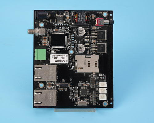
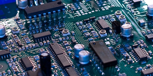
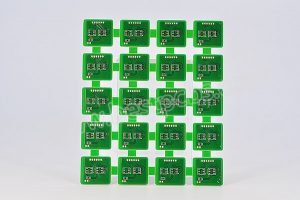
What is pcba and its components?Refers to fixing electronic components on a printed circuit board by welding or other means to form a complete circuit system with specific functions. PCBA is one of the most important components in electronic devices, providing functions such as circuit connection, protection components and heat dissipation.
Best offers consignment, full turnkey, and partial turnkey assembly services. All parts are sourced directly from manufacturers or authorized distributors such as Digikey, Mouser, Future, TTI, Avnet, and Arrow to avoid counterfeit parts.
What is PCBA?
PCBA is the abbreviation of Printed Circuit Board Assembly, which refers to the process and product of installing and soldering all necessary electronic components on a PCB (printed circuit board) to form a complete functional circuit. PCBA is a key step in the production of electronic equipment. It provides a platform for electronic components to work in a coordinated manner, enabling the device to perform its intended tasks.
What is a PCBA component?
What is a PCBA component?
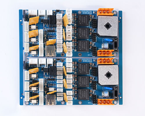
PCBA components refer to electronic components soldered on PCBs, including various components packaged in SMD patches and DIP plug-ins, such as integrated circuits IC, crystal oscillators, diodes, triodes, resistors, capacitors, transformers, digital tubes, connectors, inductors, etc. These components are the basis for realizing the hardware connection and program functions of PCBA boards. PCB designers will draw the corresponding circuit schematics according to the functions of the products and select appropriate components to realize the circuit functions.
PCBA process steps
PCBA process steps
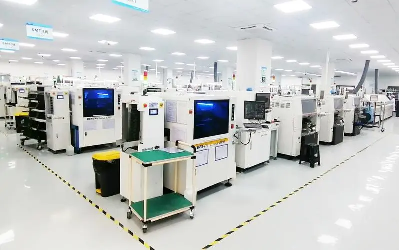
The PCBA (Printed Circuit Board Assembly) assembly process mainly includes two processes: SMT (surface mount technology) and DIP (through-hole insertion technology). According to the size and type of electronic components, the assembly process can be divided into several common component assembly methods such as single-sided mounting, double-sided mounting, single-sided mixed mounting and double-sided mixed mounting.
Empty board loading: Arrange the PCB boards neatly, put them into the material rack, and send the PCB boards to the SMT production line through the automatic board loading machine.
2. Printing solder paste: Print solder paste on the pads on the PCB board where components need to be soldered to prepare for subsequent soldering.
3.Solder paste inspection: Check the quality of solder paste printing through optical instruments to ensure that there is no problem such as too much tin, too little tin or thick solder paste.
4.SMT: Use high-speed SMT machines and general-purpose SMT machines to attach electronic components to the PCB board. Small components use high-speed SMT machines, and large components use general-purpose SMT machines.
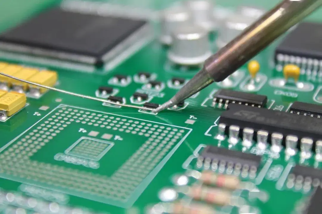
5.Reflow soldering: Melt the solder paste to solder the electronic components to the PCB board. Temperature control during the reflow soldering process is very important.
6. Cleaning and testing: Clean after soldering to remove excess solder and impurities, and then test to ensure that all components are correctly soldered.
PCB board inspection and acceptance standards
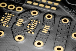
Appearance inspection: Check the dimensional accuracy, position accuracy, surface treatment and electrical safety of the PCBA board. The dimensional accuracy should meet the design requirements, such as aperture, line width, line spacing, etc. The position accuracy should be accurate and without deviation, such as component spacing, pad position, etc. The surface treatment should meet the requirements, such as whether there are scratches, oxidation, oil stains, cracks, depressions, discoloration, corrosion, etc. The electrical connection should be reliable, without short circuit or open circuit.
Acceptance conditions: The parts are damaged, but the body remains good, the internal metal components are not exposed, and the specifications are marked with text, and the polarity is identifiable. Although the IC is damaged, there is no cracking. There is no cracking between the IC foot and the body package. The part foot is not damaged. The part surface is tinned with a tin filling amount of more than 75% of the PCB board thickness. The pinhole size on the solder joint is less than 1/4 of the cross-sectional area of the part foot, and the pinhole at any point does not penetrate the PCB.
The difference between PCB and PCBA
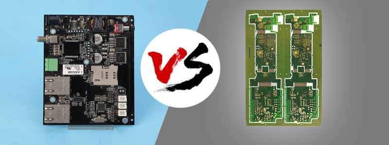
PCB is the carrier and basic framework of electronic components, while PCBA is a circuit board assembly with specific functions, which directly determines the performance and function of electronic products.
Definition and Function
1.PCB (printed circuit board): It does not contain any active or passive components itself, but is just a basic framework.
Definition: PCB is a substrate used for electrical connection of electronic components, which forms a conductive circuit pattern on an insulating substrate through etching, drilling, copper plating and other processes.
Function: PCB mainly plays the role of supporting and electrically connecting electronic components, and is the carrier of electronic components.
2.PCBA (printed circuit board assembly) PCBA is the core part of electronic products and directly determines the performance and function of the product.
Definition: PCBA is a circuit board assembly with specific functions formed by soldering electronic components to PCB through processes such as SMT (surface mount technology) or THT (through-hole mounting technology).
Function: PCBA contains PCB and all necessary electronic components, which work together to realize the preset functions of the circuit board.
Manufacturing process
1.PCB manufacturing process
Design: Design the PCB layout according to the circuit schematic.
Making the substrate: Use materials such as copper foil, insulating materials and prepreg to make the substrate of the PCB.
Etching: Remove the unnecessary copper foil part on the substrate by chemical or physical methods to form a conductive circuit pattern.
Drilling: Drill holes on the PCB for connecting different layers or installing components.
Copper plating: Plate a layer of copper in the hole and on the surface of the circuit to improve conductivity and solderability.
Subsequent processing: Including steps such as cleaning, inspection, and cutting, and finally get the finished PCB.
2.PCBA manufacturing process
Preparation: Prepare the required PCB and electronic components.
Welding: Solder the electronic components to the PCB through SMT or THT technology.
Detection: Use automated testing equipment to perform functional testing and quality inspection on PCBA.
Packaging: Package qualified PCBA for transportation and storage.
Features and applications
1.PCB features
Customization: PCB can be customized according to specific needs to meet the layout requirements of different circuits and components.
Standardization: PCB manufacturing follows certain standards and specifications to ensure product quality and reliability.
Flexibility: PCB can adapt to various complex circuit designs and component layout requirements.
Widely used: PCB is widely used in various electronic products, such as mobile phones, computers, home appliances, etc.
- PCBA features
Functionality: PCBA has specific functions and can be directly used for the assembly and testing of electronic products.
Integrity: PCBA contains all the necessary electronic components and PCBs, and is a complete circuit board assembly.
Reliability: After rigorous testing and inspection, PCBA has high reliability and stability.
Specific application: PCBA is usually used on the production line of electronic products and directly participates in the assembly and testing process of the product.
The difference between PCBA and SMT
PCBA VS SMT
There are significant differences between PCBA processing and SMT processing in terms of definition and scope, component types and assembly methods, process flow and equipment, application fields and product features.
Definition and scope
PCBA processing is a broader concept that covers the entire process of assembling electronic components onto printed circuit boards, including circuit board design, component selection, welding, testing and other links. PCBA processing can use both through-hole technology (THT) and surface mount technology (SMT).
SMT processing is an important link in PCBA processing, specifically referring to the process of mounting surface mount components (such as chip resistors, chip capacitors, etc.) on the surface of printed circuit boards using surface mount technology. SMT processing usually includes steps such as printing solder paste, mounting components, and reflow soldering.
Component types and assembly methods
PCBA processing can handle various types of components, including through-hole components (such as integrated circuits in DIP packages) and surface mount components. Through-hole components need to be soldered to the other side of the circuit board through the jack, while surface mount components are directly mounted on the surface of the circuit board.
SMT processing focuses on processing surface mount components. These components have the characteristics of small size, light weight, no pins or short pins, which can achieve high-density assembly, thereby improving the integration and performance of circuit boards.
Process flow and equipment
The application field of PCBA processing is very wide, covering almost all industries that require electronic circuit boards, such as communications, medical, aviation, home appliances, etc. Since PCBA processing can handle various types of components and complex assembly requirements, it is suitable for the production of electronic products of various sizes and complexities.
SMT processing is more suitable for the production of miniaturized, lightweight, and highly integrated electronic products. Since surface mount components are small and light, SMT processing can achieve high-density assembly, thereby reducing product volume and weight. In addition, SMT processing also has the advantages of high production efficiency and stable product quality.
PCBA Common Terms
Surface mount assembly (SMA): a printed circuit board assembly completed using surface mount technology.
Reflow soldering: the connection between surface mount components and PCB pads is achieved by melting the solder paste pre-allocated to the PCB pads.
Wave soldering: the molten solder is sprayed into a solder wave crest as required by the design through the equipment, so that the PCB with electronic components passes through the solder wave crest to achieve the connection between the components and the PCB pads.
Solder paste printing: the solder paste is placed on the steel mesh, and the solder paste is leaked through the holes on the steel mesh by a scraper and accurately printed on the PCB pads.
Automated optical inspection (AOI): the soldering effect of the PCB board can be detected by scanning and comparing. Defective PCB boards can be detected.
Rework: the act of reworking defective boards detected by AOI or manual inspection.
Fine pitch: refers to the lead center spacing of surface mounted package components ≤ 0.50mm.
Gerber file: A collection of document formats that describe circuit board images and drilling and milling data, used for PCBA quotation and processing.
BOM file: A bill of materials that lists all materials and quantities required for PCBA processing.
Solder paste deviation, solder paste tip, solder paste hole, etc.: These are common defects in PCBA processing.
FAQ About PCBA
FAQ Abaout PCBA
Why can PCBA processing improve the reliability and stability of circuit boards? PCBA processing can greatly reduce the failure rate of products, speed up the launch of products, and improve production efficiency through strict quality management system, strict control and quality inspection from component procurement to production process.
How to ensure the quality of PCBA? The key to ensuring the quality of PCBA lies in a strict quality management system, including strict control and quality inspection from component procurement to production process.
How to control the cost of PCBA processing? Methods to control the cost of PCBA processing include optimizing design, reducing component costs, and improving production efficiency.
How to choose a suitable PCBA processing plant? Selecting a PCBA processing plant requires considering factors such as the factory’s equipment, quality management system, production capacity, and experience.
What are the problems and causes of cold soldering in PCBA? Due to insufficient solder paste, insufficient soldering temperature, or too short soldering time, no effective soldering is formed between the component pins and the pads, which may cause circuit blockage or poor contact.
What are the problems and causes of cold welding?
Due to the low welding temperature, the welding material is not completely melted, which is manifested as the surface of the welding point is rough, gray, and has no gloss. The welding strength is insufficient, which can easily cause the welding point to break.
What are the problems and causes of continuous welding?
Due to excessive application of solder paste or the pins of adjacent components are too close, a connection is formed between welding points that should not be connected, which may cause a short circuit.
What are the problems and causes of component damage?
Due to static electricity, overheating, mechanical stress and other reasons, the performance of components is reduced or completely fails, affecting the overall circuit function.
What are the problems and causes of component misalignment?
Due to equipment failure, operating errors and other reasons during the patch process, the components are not aligned with the pads on the PCB, which may cause poor welding or abnormal circuit function.
What are the problems and causes of PCB contamination?
During the production and storage process, it is polluted by oil stains, dust and other pollutants, which affects the welding effect and may cause problems such as poor welding or short circuit.
What are the problems and causes of PCB deformation?
Due to environmental factors such as high temperature and humidity, PCB deformation affects the mounting and welding of components, which may cause abnormal circuit function.
What are the problems and causes of missed inspection of PCBA?
Due to failure of detection equipment, operating errors, etc., defective products may flow into the next process or market, affecting product quality and customer satisfaction.
What are the problems and causes of PCBA mixing?
During the production process, components or PCBs are mixed, resulting in product performance not meeting requirements, which may cause customer returns or claims.
You may also like


Tags: PCBA