
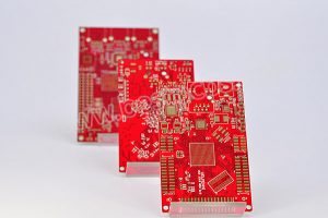
High density interconnect (HDI) technology plays a pivotal role in the electronics field, and high-density interconnect boards are the core embodiment of this technology. As a key connection carrier between electronic components, it is an important guarantee for realizing miniaturization, high performance and multi-functionality of electronic equipment.
What are high density interconnects?
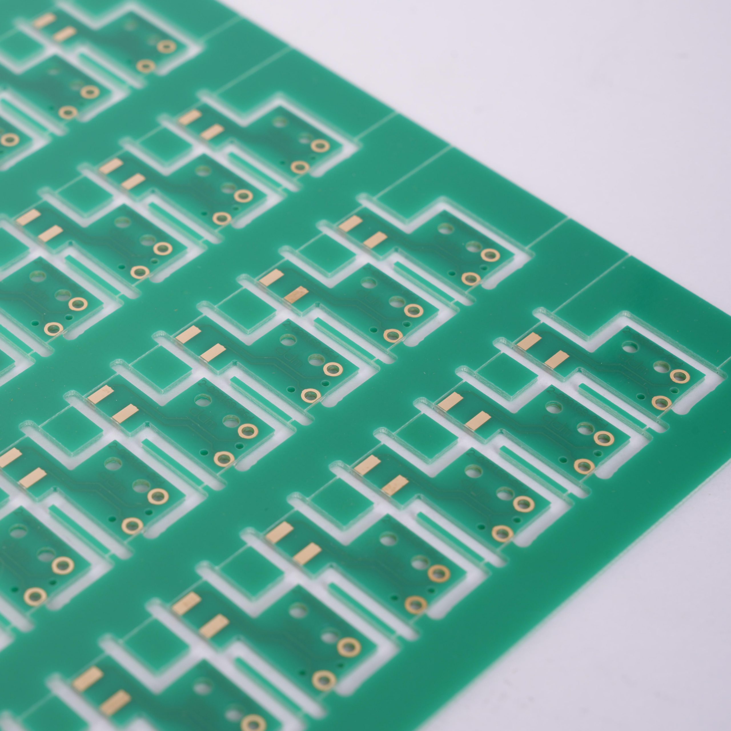
High-density interconnect (HDI) is a printed circuit board (PCB) manufactured using higher-density wiring technology. Compared with traditional PCB, HDI board achieves miniaturization, lightweight and higher wiring density of circuit board through smaller aperture, finer line width/spacing and more layers of blind and buried hole technology to adapt to Electronic devices, especially mobile devices, require efficient space utilization and high-performance transmission.
The core of HDI technology lies in its high-density wiring design. By increasing the number of PCB layers, reducing wire width and spacing, and using micro-hole (such as laser drilling) processes, HDI technology significantly increases circuit complexity and wiring density. This technology is often used in electronic products such as smartphones, tablets, and smart wearable devices, meeting the needs of these devices for efficient space utilization and high-performance transmission.
What is the difference between PCB and HDI?
The main differences between PCB and HDI boards lie in wiring density, manufacturing process, size and cost. HDI boards use high-density interconnection technology, with higher wiring density and more complex circuit layouts, while ordinary PCBs are relatively simple and suitable for some application scenarios that do not require high line density.
There are significant differences between HDI boards and ordinary PCBs in terms of wiring density, manufacturing process, size and cost. HDI boards use high-density interconnection technology, with higher wiring density and more complex circuit designs, enabling smaller size and lighter design requirements. In comparison, the wiring density of ordinary PCB is low, which is suitable for some application scenarios that do not require high line density.
In terms of manufacturing process, HDI boards use more advanced manufacturing processes, including laser drilling, stacked copper plates and etching technology, to achieve high-density interconnection and complex circuit wiring. In comparison, the manufacturing process of ordinary PCBs is relatively simple, usually using photolithography and etching processes.
Because HDI boards have higher circuit density and complex circuit layouts, their size and thickness are usually smaller, making them suitable for applications that require compact packaging and space constraints. Ordinary PCBs do not have these restrictions and are suitable for more diverse application scenarios.
In terms of cost, since the manufacturing process of HDI boards is more complex and has higher technical requirements, its manufacturing cost is relatively high. In comparison, ordinary PCBs have lower manufacturing costs and are suitable for some application scenarios that do not have high circuit density and technical requirements.
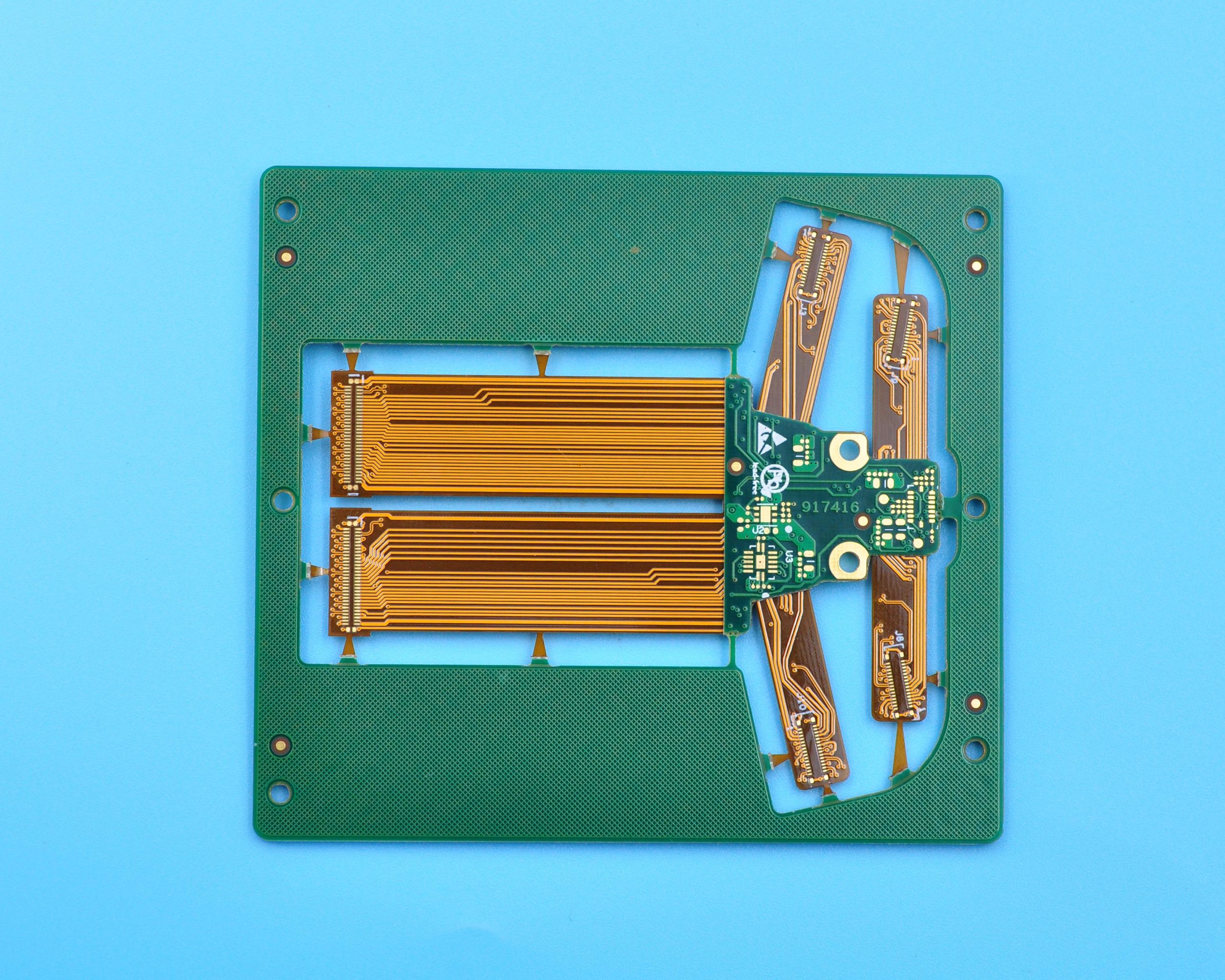
What is the structure of HDI PCB?
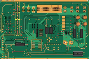
The structure of HDI PCB mainly includes inner laminate, outer laminate, gaskets, blind and buried vias and other components.
The inner laminate is the core part of the HDI circuit board. It is composed of multiple layers of conductive materials and insulating materials alternately stacked. It mainly realizes the transmission and control of circuit signals. The number of layers of the inner laminate can be very high. It uses microporous technology to achieve a high-density circuit layout and has excellent electrical performance and stability.
The outer laminate is located on the outside of the inner laminate and is also composed of multiple layers of conductive materials and insulating materials alternately stacked. Its main function is to protect the internal circuit from the influence of the external environment, such as humidity, temperature, mechanical stress, etc. The outer laminate can also provide additional grounding and shielding to improve circuit performance and reliability.
The gasket is an insulating material used to connect the inner laminate and the outer laminate. Its main function is to isolate the inner and outer laminates, prevent electrical interference, and provide certain mechanical support to ensure the stability of the circuit board.
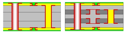
A blind buried via is a non-penetrating through hole located inside the inner laminate. It is not directly connected to the outer laminate and mainly realizes the electrical connection between the inner laminates. Blind and buried vias do not penetrate the entire circuit board, which can effectively reduce the thickness and weight of the circuit board and improve the circuit board’s thermal resistance and mechanical stress resistance.
What are the advantages of HDI PCB?
The main advantages of HDI PCB include high-density interconnection, optimized wiring design, good signal transmission performance, high reliability and stability, smaller size and weight, and higher production efficiency.
First, HDI PCB achieves higher line density by using higher-level packaging technology and smaller apertures. This means that under the same board size, HDI PCB can accommodate more electronic components and complex circuit designs, thereby improving the performance of the product.
Second, the design of HDI PCB is more compact. Through multi-layer wiring and micro-via technology, the size and weight of the circuit board can be greatly reduced, adapting to the trend of modern electronic devices to pursue thinness and shortness.
Finally, the production process of HDI PCB is more efficient, and advanced technologies such as laser opening, thin film transformer, and cover packaging are used to achieve high-efficiency production.
What are the disadvantages of HDI PCB?
- 1. Difficulty in impedance control: The complexity of pattern transfer and electroplating processes increases production difficulty, which may lead to unstable impedance values.
- 2. Complex production cost control: The high-density circuit part of HDI PCB has a slow etching speed, which leads to excessive etching of isolation lines and increases production costs.
- 3. Environmental impact: During the electroplating and etching process, a large amount of copper ions enter the waste liquid, causing environmental pollution and difficulty in recycling.
- 4. High difficulty in design and manufacturing: HDI PCB is manufactured using micro-blind buried via technology and built-up method. The technical requirements are high and the process is complex, which increases the difficulty of design and manufacturing.
- 5. High material costs: The materials used in HDI PCB, such as PI and other high-performance materials, are more expensive, increasing manufacturing costs.
- 6. Quality issues: HDI PCB is prone to problems such as poor solderability and delamination during the manufacturing process. These problems may require higher process capabilities and quality control to avoid.
What are the applications of HDI PCB?
HDI PCB (High Density Interconnect PCB) can greatly reduce the size and weight without sacrificing performance by using microvias and tiny line widths and spacing, and is particularly suitable for portable electronic devices.
The main application areas of HDI PCB include:
- Communication field: HDI PCB can achieve higher data transmission rates and lower energy consumption by increasing the number of tiny components.
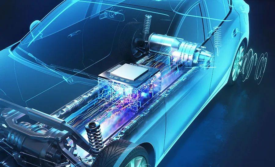
- Automotive Electronics: HDI PCB reduces product volume and production costs in the high integration of automotive electronic products, ensuring the stable operation of automotive electronic products.
- Medical Equipment: HDI PCB is widely used in high-precision and high-stability medical equipment, improving the accuracy, sensitivity and stability of the equipment.
- Mobile Communication: HDI PCB supports high-speed data transmission, maintains stable signal transmission, and supports a variety of wireless communication technologies.
- High Performance Computing (HPC): HDI PCB provides efficient interconnection channels, significantly improving computing performance and response speed.
In short, high-density interconnection circuit boards, as an important embodiment of high-density interconnection technology, play an irreplaceable role in the development of modern electronic technology. With the continuous advancement of technology, its future development prospects are still very broad, and it will continue to promote the development of electronic devices in the direction of smaller, stronger, and smarter.
You may also like


Tags: PCB