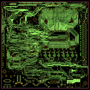
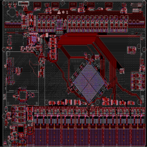
If you’re working with electronics, you’ve probably heard of Printed Circuit Boards (PCBs). They’re at the heart of almost every electronic device we use today. But have you ever wondered what are PCB designs called? Are they just called PCB designs, or is there more to it? Well, it turns out there are quite a few terms for PCB designs, and each one refers to a specific aspect of the design process. Let’s take a closer look at these terms, how they’re used, and what makes each one unique.

What Are PCB Designs Called?
PCB designs are often referred to by different names depending on the context or the stage of the design process. Let’s explore the most common terms:
1. PCB Layout
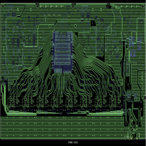
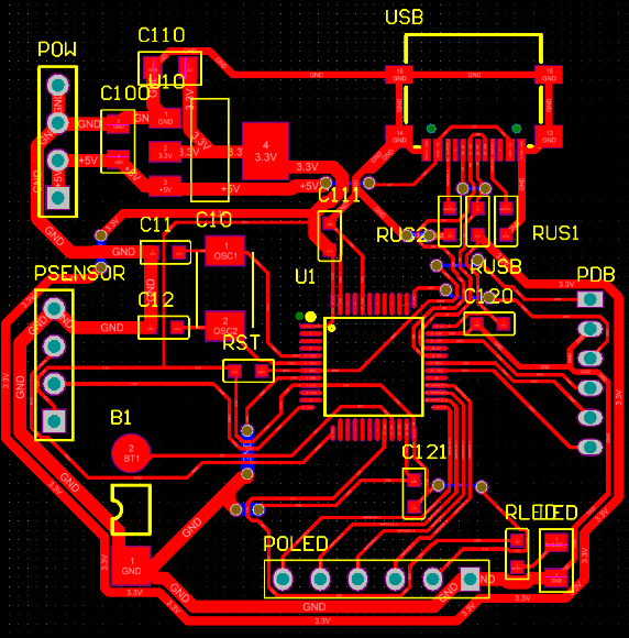
This is probably the most frequently used term. When someone mentions a PCB layout, they’re talking about the physical arrangement of components and the routing of electrical connections (also called traces) on the board.
Think of it like designing the floor plan of a house. The layout ensures that everything fits within the available space and that all the rooms (or in this case, components) are connected in the right way.
2. Circuit Board Design
Sometimes, you’ll hear people refer to the process as circuit board design. This term emphasizes the broader design aspect, from planning the circuit to placing components and routing connections. It’s a more general term that covers everything from the initial schematic to the final layout.
3. PCB Schematic
While the schematic is technically just one part of the design process, some people refer to the entire design as the schematic. This is more common among those who focus on the circuit’s logic rather than its physical structure.
4. Gerber Files
Once the design is complete, it’s converted into a set of files called Gerber files. These files contain all the information needed to manufacture the PCB. Sometimes, people use the term Gerber files to refer to the finished design, even though it’s technically just the output.
5. EDA (Electronic Design Automation) File
In professional environments, PCB designs are often called EDA files. These are the files created by design software like Altium Designer, KiCad, or Eagle. They contain all the details of the design, including the schematic, layout, and design rules.
What Is the Difference Between a PCB Design and a Schematic Design?
Many people use the terms PCB design and schematic design interchangeably, but they serve different purposes in the design process.
Schematic Design
- Represents the electrical connections between components.
- Focuses on the logic and functionality of the circuit.
- Uses symbols to represent components like resistors, capacitors, and transistors.
- Helps engineers understand how the circuit works.
PCB Design
- Translates the schematic into a physical layout.
- Focuses on the placement of components and routing of traces.
- Considers factors like board size, layer count, and thermal performance.
- Ensures the circuit can be manufactured and assembled.
In summary, the schematic shows what the circuit does, while the PCB design shows how it does it physically.
PCB Schematics Elements
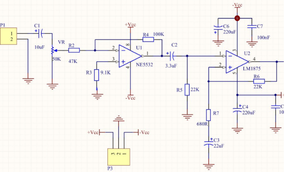
A schematic is the starting point for any PCB design. It provides a clear visual representation of the circuit’s functionality. Here are the key elements of a schematic:
1. Component Symbols
Each component in the circuit is represented by a symbol. For example, a resistor is usually shown as a zigzag line, while a capacitor is two parallel lines.
2. Nets (Connections)
Lines connecting the symbols represent electrical connections, known as nets. These nets define how components interact with each other.
3. Reference Designators
Lines connecting the symbols represent electrical connections, known as nets. These nets define how components interact with each other.
4. Values and Ratings
The schematic also shows the values and ratings of components, such as the resistance of a resistor or the capacitance of a capacitor.
5. Power and Ground Symbols
Every circuit needs power and ground connections. These are represented by standard symbols, ensuring the circuit has a common reference point for voltage.
Common Terms in PCB Design
1. Silkscreen Layer
The silkscreen layer contains text, logos, and symbols printed on the surface of the PCB to help identify components and guide assembly. It can also include part numbers, component values, and polarity markings.
2. Via
A via is a hole in the PCB that allows electrical connections between different layers. Vias are often used in multi-layer PCBs to route signals between the top and bottom layers or inner layers.
3. Copper Pour
A copper pour is a large, solid region of copper that is poured over areas like ground or power planes. It helps reduce noise, increase current-carrying capacity, and improve thermal dissipation.
4. Trace Width
Trace width refers to the thickness of the copper traces used to connect components. The width of a trace must be designed to carry the required amount of current without overheating.
5. Drill Hole
A drill hole is a hole that is made in the PCB to accommodate components with leads or for vias. The size and placement of drill holes are critical to the assembly process.
6. Solder Mask
The solder mask is a protective layer applied over the PCB to prevent solder from bridging between pads. It also helps prevent oxidation of the copper traces and improves the board’s overall durability.
7. Pad
Pads are small copper areas on the PCB where components are mounted or soldered. Pads can be through-hole or surface-mount, depending on the type of component.
8. Bill of Materials (BOM)
The BOM is a comprehensive list of all the components required for the assembly of a PCB. It includes details like part numbers, quantities, and specifications for each component.
9. Impedance Control
Impedance control is the process of ensuring that the impedance of the PCB traces matches the requirements of the signals that will travel through them. This is important for high-speed and RF circuits.
10. Stack-up
Stack-up refers to the arrangement of layers in a multi-layer PCB. It defines how the copper, dielectric, and other materials are stacked to create the board.
11. Daisy-Chaining
Daisy-chaining is a method of connecting multiple components or pins in a series, often used in signal or power distribution systems within the PCB design.
12. Overcurrent Protection
Overcurrent protection refers to circuits designed to prevent excessive current from flowing through the PCB traces, often by using fuses or resistors that limit the current flow.
13. Design for Manufacturability (DFM)
DFM refers to designing the PCB in a way that makes it easier and more cost-effective to manufacture. This includes factors like trace width, pad size, and component placement.
14. Routing
Routing is the process of designing the electrical paths that connect the components on a PCB. Proper routing ensures that signals are carried efficiently with minimal interference.
15. Thermal Via
Thermal vias are specially designed vias used to transfer heat away from high-heat components to other parts of the PCB or a heat sink.
16. Electromagnetic Interference (EMI) Shielding
EMI shielding involves using design techniques, such as grounding and the use of shielding components, to protect sensitive parts of the PCB from electromagnetic interference.
17. Differential Pair
A differential pair is a set of two traces that carry complementary signals, often used in high-speed designs like USB or Ethernet to minimize noise and improve signal integrity.
18. Power Distribution Network (PDN)
The PDN refers to the system of traces and planes that deliver power to various components on the PCB. Proper PDN design is crucial to ensure reliable power delivery and minimize voltage drops.
19. Electrical Rule Check (ERC)
ERC is a process that checks the schematic design for electrical issues like unconnected nets, incorrect component connections, or incorrect power supply connections.
20. Multi-layer PCB
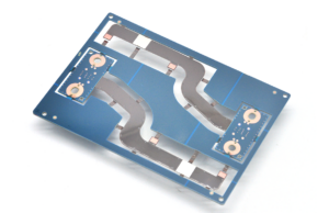
A multi-layer PCB contains more than two layers of conductive material and is used for more complex designs that require high-density circuits, especially in smaller devices.
21. Surface-Mount Technology (SMT)
SMT is a method for mounting components directly onto the surface of the PCB, rather than inserting them through holes. This allows for smaller, more compact designs.
22. Through-Hole Technology
Through-hole technology involves inserting component leads through holes in the PCB and soldering them on the opposite side. It’s commonly used for components that require strong mechanical bonds.
23. Hot Air Soldering
A method of soldering components onto the PCB using hot air, often used in reflow soldering processes for surface-mount components.
24. Trace Routing
Trace routing is the process of laying out the paths that the electrical signals will take through the PCB. Good trace routing ensures efficient and reliable signal transmission.
25. Tenting
Tenting refers to the process of covering the vias with a layer of solder mask, leaving the pad open. It helps prevent solder from flowing into vias during soldering.
PCB Design vs. PCB Layout
Although often used interchangeably, PCB design and PCB layout have different meanings:
PCB Design: Refers to the entire process, from schematic creation to generating manufacturing files.
PCB Layout: Specifically focuses on the physical arrangement of components and routing of traces on the board.
In simple terms, PCB layout is a part of the overall PCB design process.
PCB Design Process
Designing a PCB is a multi-step process that requires careful planning and attention to detail.
1. Schematic Capture
The process starts with creating a schematic diagram that defines the circuit’s functionality and connections.
2. Component Selection
Next, components are selected based on the circuit requirements. Factors like size, power rating, and cost are considered.
3. PCB Layout
Components are placed on the board, and traces are routed to connect them. This step requires balancing electrical performance with physical constraints.
4. Design Rules Check (DRC)
The layout is checked for errors or violations of design rules to ensure it meets manufacturing standards.
5. Gerber File Generation
Once the design is complete, Gerber files are generated. These files are used by manufacturers to produce the PCB.
6. Fabrication and Assembly
The PCB is fabricated, and components are assembled to create the final product.
FAQs
Q: What software is used for PCB design?
A: Popular software includes Altium Designer, Eagle, KiCad, and OrCAD.
Q: How many layers can a PCB have?
A: PCBs can have anywhere from one to 16 or more layers, depending on complexity.
Q: Why is trace width important?
A: Trace width affects the current-carrying capacity and signal integrity of the circuit.
Q: What is a multilayer PCB?
A: A multilayer PCB has multiple layers of copper separated by insulating material, allowing for more complex designs.
Q: How long does it take to design a PCB?
A: The time varies based on complexity. Simple designs may take a few days, while complex designs can take weeks.


