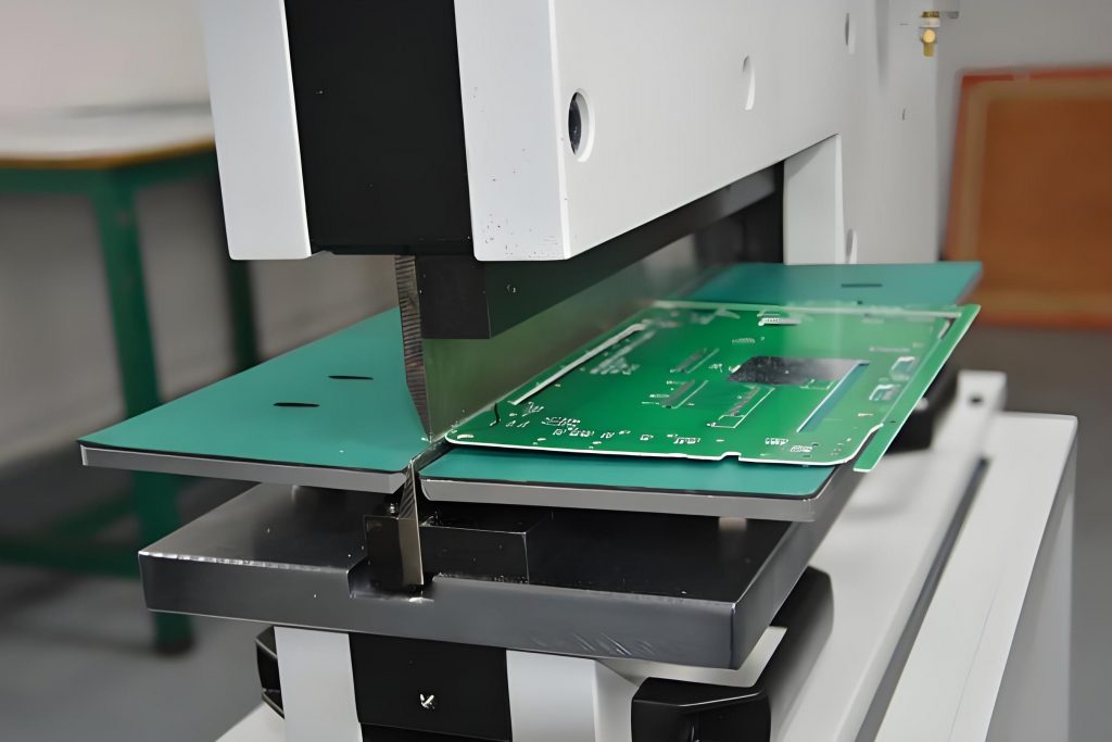
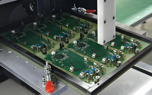
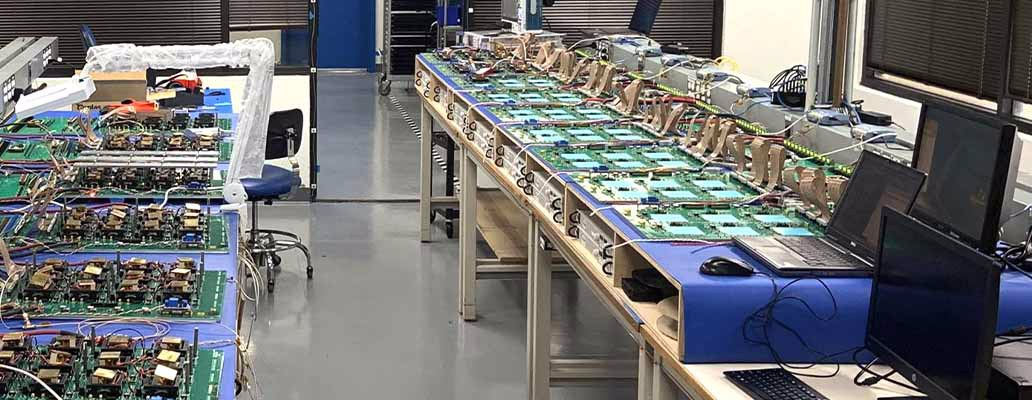
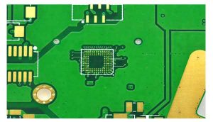
V-CUT cuts a V-shaped groove on the PCB board, so that the board can be easily separated in subsequent processing, while the stamp hole sets a small hole on the edge of the board, making the board more neat and stable when separated, which can provide higher space utilization and better signal transmission performance. The combination of these two technologies not only improves production efficiency, but also ensures product quality and reliability.
What is PCB V-CUT?
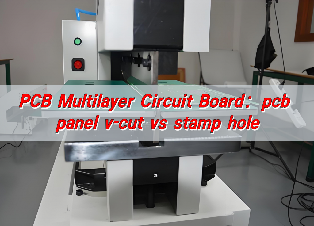
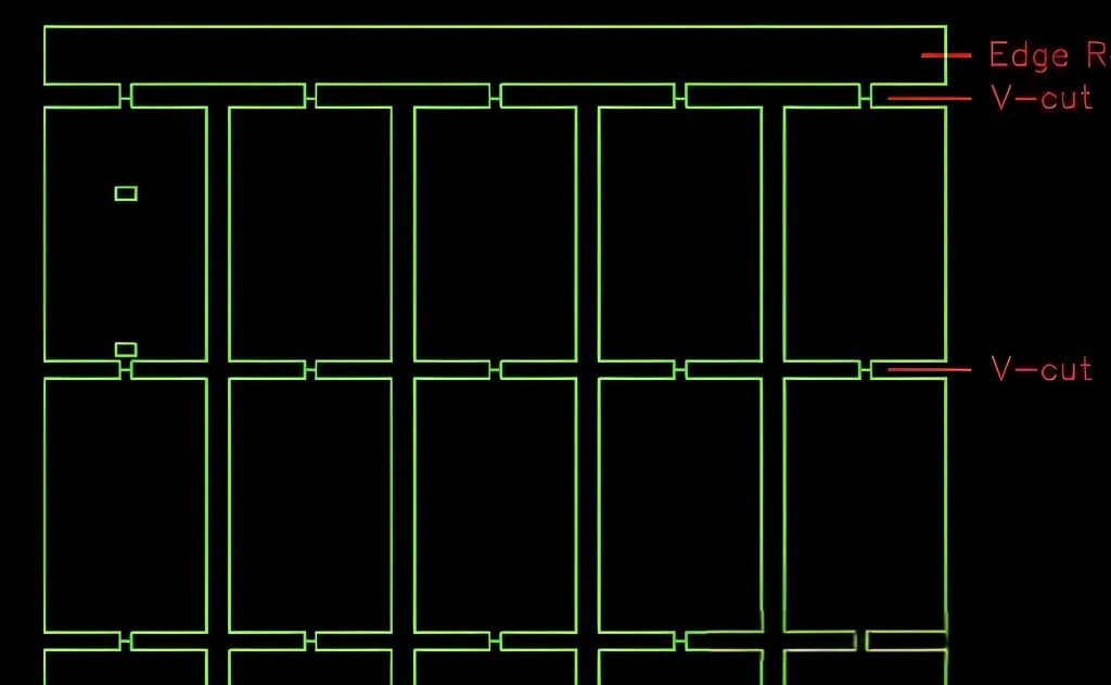
PCB V-CUT is a technology that cuts a V-shaped groove on a printed circuit board, which is mainly used to facilitate subsequent board separation operations. V-CUT is to cut a series of V-shaped cuts on the PCB board and then break the board after applying appropriate force, thereby dividing the multilayer PCB into separate panels.
The role and importance of V-CUT
- Improve manufacturing efficiency: In mass production, V-CUT can quickly divide large boards into multiple small panels to meet the needs of mass production.
- Reduce material waste: Through V-CUT cutting, raw materials can be maximized, waste generation can be reduced, and production costs can be reduced.
- Convenient assembly: V-CUT allows the separated small panels to be easily assembled and welded, improving production efficiency.
V-Cut is widely used in the batch manufacturing of multi-layer PCBs, especially when a large board needs to be divided into multiple small panels.
What are the advantages and disadvantages of V-Cut?
Advantages of V-Cut:
- Easy to operate: The V-Cut design can facilitate the separation of SMT circuit boards after assembly, avoiding PCB bending and damage to electronic components that may be caused by manual separation.
- Improve production efficiency: When assembling the edges of two boards, the efficiency of SMT patch lines and wave soldering can be significantly improved.
- Wide range of applications: V-Cut is suitable for regular PCB boards, especially in batch production, the use of V-Cut can significantly improve production efficiency.
Disadvantages of V-Cut:
- Can only cut straight lines: V-Cut can only cut straight lines, and it can only cut straight lines from one end to the end, and cannot be changed in the middle. If there is a 90-degree or other angle bend in the middle, it is not allowed.
- High requirements for tools: The material and manufacturing process of V-Cut knives have a great influence on the cutting effect. For example, high-speed tool steel V-Cut knives are not wear-resistant and need to be frequently changed and sharpened, which affects production efficiency; alloy-inlaid V-Cut knives increase the brittleness of the blade due to welding, and the quality is difficult to guarantee, and the tooth breakage rate is high.
- Restrictions on PCB thickness: PCB boards that are too thin or too thick are not suitable for V-Cut, because too thin boards are easy to break and too thick boards are difficult to cut.
What is a stamp hole?
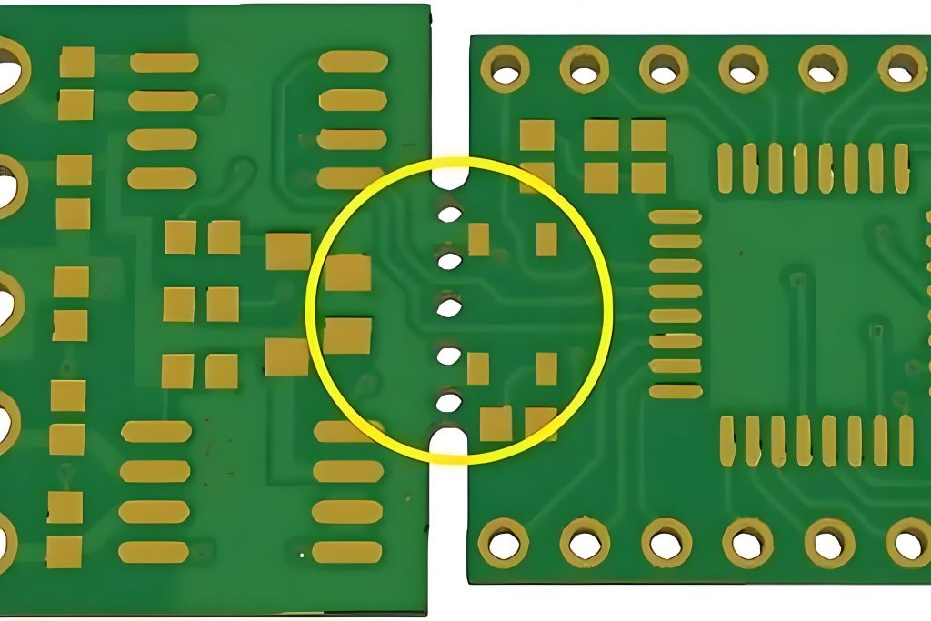
A stamp hole refers to a hole on the motherboard panel that is used to connect small PCBs that make up the array together and to easily remove components from the PCB. Stamp holes are perforated, and when pushed down, the holes break, allowing components to be removed without damaging the PCB itself.
The specific functions of stamp holes include:
- Connecting small PCB boards: When there are multiple small PCBs that need to be connected and connectors cannot be used, they can be connected through stamp holes. Perforations allow current to flow through the PCB and connect with other nearby PCBs.
- Transmit power and data: Stamp holes can transmit power and data between two different PCBs or devices to achieve communication between devices.
Design requirements for stamp holes include:
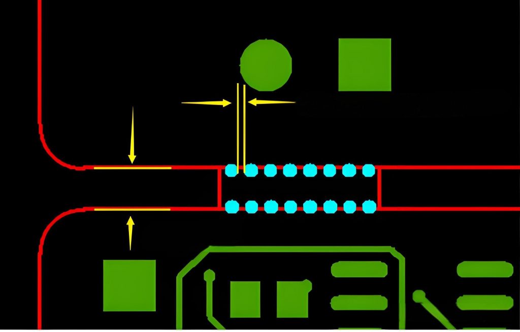
- Number of holes: Usually stamp holes are in groups of 5 to connect components together, but the specific number may vary depending on the PCB design.
- Size: The size of stamp holes is usually 0.020 inches or 0.5 mm in diameter, and the specific size will vary depending on the PCB design.
- Hole spacing: The spacing of stamp holes is usually 0.030 inches or 0.76 mm to prevent components from being too close and causing short circuits.
In addition, design tips for stamp holes include:
- Sufficient pull tabs: In order to maintain the integrity of the PCB, the pull tabs should be strong enough to support the weight of the components above.
- Stay away from sensitive components: Stamp holes should be away from sensitive components to avoid electrical short circuits caused by damage to the pull tabs.
- Spacing: The spacing between two stamp holes should be between 60mm-90mm to facilitate the installation of components.
What are the advantages and disadvantages of stamp holes?
The advantages of stamp holes include:
- Improved production efficiency: Stamp holes can connect multiple small-sized PCBs together for production and processing, thereby simplifying the production process and reducing costs.
- Convenient assembly and disassembly: In situations where detachable connections are required, such as modular designs, stamp hole connections can achieve convenient assembly and disassembly, facilitating product repair and upgrades.
- Reduced space occupation: The stamp hole design can greatly reduce the required space, especially suitable for compact designs.
- Improved signal transmission performance: Stamp holes shorten the signal path, reduce signal delay and cross interference, and are suitable for complex multi-layer board designs.
Disadvantages of stamp holes include:
- Possible cost increase: The design of stamp holes will increase certain costs because holes need to be reserved on the PCB, and the size of these holes will also be included in the overall size of the PCB.
- The broken surface is not easy to control: Stamp holes are separated by breaking, and the broken surface is not easy to control accurately, which may cause line damage or even scrap.
What is the difference between V-Cut and stamp hole?
The main difference between V-Cut and stamp hole lies in their definition, purpose and applicable scenarios.
- V-Cut: V-Cut is to pre-cut a V-shaped dividing line at a specific position of the PCB, which is usually used to facilitate the de-paneling (De-paneling) of the SMT circuit board after assembly. The dividing line of V-Cut is generally a straight line, without complex curves or arcs, and is suitable for panel connection of conventional PCB boards.
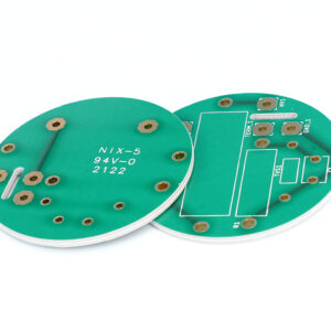
- Stamp hole: Stamp hole is to connect the process edge and the PCB board by punching a series of circular holes shaped like stamps on the PCB board. It is mainly used for irregular shaped PCB boards, such as circles. Since V-Cut cannot achieve this connection, stamp holes are more used in special-shaped boards.
How to choose a suitable PCB de-paneling method?
Choosing a suitable PCB de-paneling method requires considering multiple factors, including the shape of the PCB, the scale of production, the cost budget, and the requirements for product quality.
1. V-CUT (V-shaped cutting):
- Advantages: low cost, simple operation, fast speed, suitable for regular shaped PCBs arranged in a straight line.
- Disadvantages: only straight line de-paneling can be performed, which is not suitable for complex or irregular shaped PCBs.
- Applicable scenarios: suitable for small and medium batch production, and the PCB shape is relatively regular.
2. Stamp hole:
- Advantages: Suitable for irregular shaped PCBs, such as round or special-shaped boards, and can provide better space utilization.
- Disadvantages: Compared with V-CUT, the cost is slightly higher, and some burrs may be generated during the separation process.
- Applicable scenarios: Suitable for PCBs with complex or irregular shapes, and production that requires high space utilization.
3. Milling cutter type board separation:
- Advantages: It can be divided into boards of any shape, with smooth cutting edges and low stress, and is suitable for PCBs of various shapes.
- Disadvantages: The initial cost is high, and the equipment and operation are relatively complex.
- Applicable scenarios: Suitable for complex-shaped PCBs with high cutting accuracy requirements.
4. Laser board separation:
- Advantages: High precision, suitable for PCBs with complex shapes and high precision requirements.
- Disadvantages: High cost and slow speed.
- Applicable scenarios: Suitable for small-batch production with high precision requirements.
When choosing a board separation method, factors such as the specific needs of the product, production costs, production efficiency, and requirements for product quality should be comprehensively considered to ensure that the most appropriate board separation method is selected.
In summary, both have their own advantages and disadvantages. V-CUT is particularly suitable for regular-shaped PCB boards with its low cost and high efficiency, while stamp holes show unique advantages when dealing with irregular-shaped boards or boards that require higher space utilization. We need to choose the most suitable PCB depaneling solution according to the actual situation.
BEST Techbology has rich experience and advanced equipment, and can flexibly apply a variety of depaneling technologies such as V-CUT and stamp holes to meet the needs of different customers. Whether your PCB design is regular or complex, please feel free to contact us at sales@bestpcbs.com to get the best solution.


