The birth and development of FPC (Flexible Printed Circuit) and PCB (Printed Circuit Board) have given rise to a new product called the rigid flex PCB. Therefore, a flexible-rigid combination board is a circuit board that combines a flexible circuit with a rigid circuit through processes such as lamination, according to relevant technical requirements, resulting in a circuit board that possesses both the characteristics of FPC and PCB.
What Is Rigid Flex PCB?
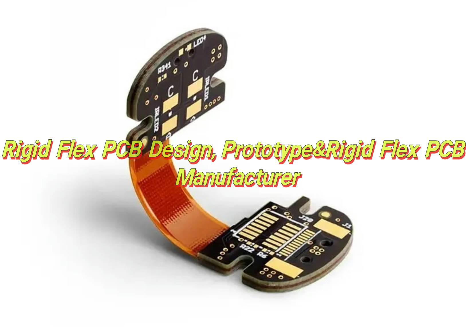
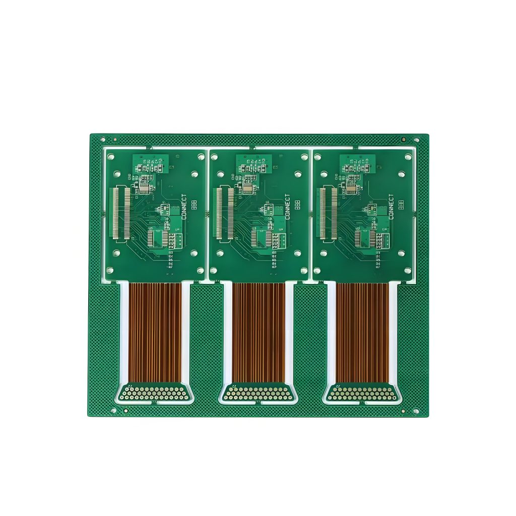
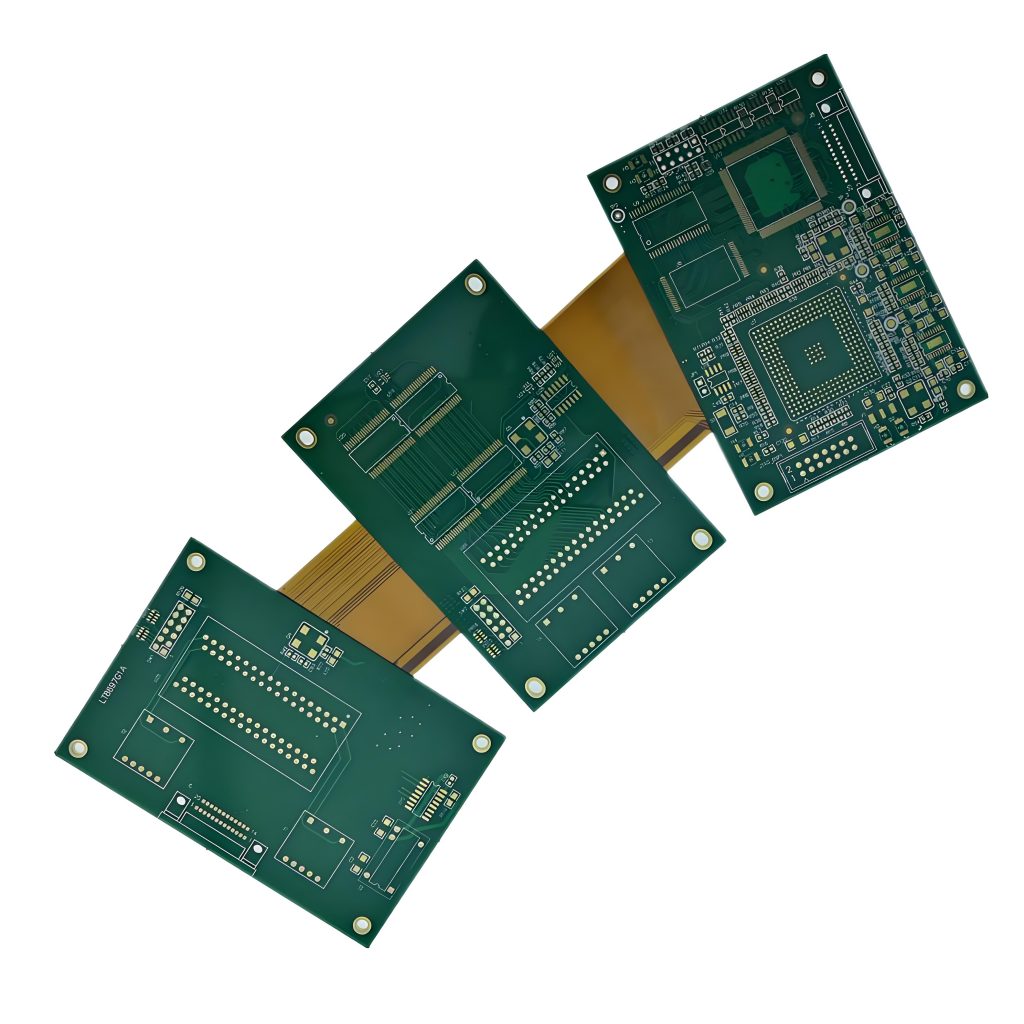
A rigid flex PCB is a composite type of circuit board that combines flexible printed circuit boards (FPC) with rigid printed circuit boards (PCB) through specific processes. It integrates the flexibility of FPC and the rigidity of PCB, possessing both characteristics of FPC and PCB. It can be folded or bent to reduce space occupation and can solder complex components, offering higher stability and reliability.
Best technology focus on high quality rigid-flex PCB design, prototype and manufacturing over 18 years. So we can flexibly handle various emergencies encountered in production based on our rich work experience to achieve fast delivery. Meanwhile, we have our own complete PCB manufacturing industry chain and advanced production machines, so we can control the cost of the entire production process well and provide customers with high-quality products at competitive prices. Please feel free to contact us at sales@bestpcbs.com if you have any request for rigid flex PCB.
Rigid Flex PCB Layer Stackup
1. Basic layered architecture
The stacked structure of the rigid-flexible board achieves functional partitioning through the alternating combination of rigid materials and flexible materials:
- Outer rigid layer: Usually uses FR4 fiberglass board to provide mechanical support and component installation stability, while achieving electrical isolation.
- Intermediate flexible layer: It is composed of polyimide (PI) film or polyester (PET), and is combined with rolled & annealed copper or electrolytic copper to form a conductive line to achieve bending connection function.
- Adhesive layer: Use thermosetting adhesive (such as epoxy resin) or low-flow adhesive semi-cured sheet to seamlessly combine the rigid layer and the flexible layer to enhance structural stability.
- Typical example:
Five-layer structure (5-4-1 type): outer rigid board → thermosetting adhesive → inner electrical layer rigid board → thermosetting adhesive → middle signal layer flexible board → thermosetting adhesive → outer rigid board
Four-layer structure: double-layer FPC substrate + gold finger interface + FR4 filling area + hollow layered design, taking into account plug-in stability and flexibility.
2. Material configuration and function
- Rigid substrate
FR4 fiberglass board: high temperature resistance, good insulation, thickness 0.2–3.2 mm, used for support and heat dissipation.
- Flexible substrate
Polyimide (PI) film: high temperature resistance (>300°C), low deformation, thickness 12.7–127μm, suitable for dynamic bending scenarios.
- Conductive layer
Rolled copper (smooth and ductile) or electrolytic copper (low cost), thickness 12–35 μm, used for signal transmission.
- Protective layer
Coverlay: PI or PET material, thickness 12.7–127 μm, moisture-proof, anti-pollution and solder-resistant.
3. Layer classification and typical application
- Single-sided board
Structural features: There is a conductive circuit layer on only one side, and the other side is covered with a substrate or insulating ink, which is transparent under strong light (excluding special process requirements).
Application scenarios: Simple circuit connection scenarios, such as low-complexity sensor modules.
- Double-sided board
Structural features: There are conductive circuit layers on both sides, and the electrical connection between layers is achieved through metallized holes (PTH holes).
Application scenarios: General electronic devices, such as basic communication modules.
- Multi-layer board
Definition: 3 or more circuit layers are superimposed through a “sandwich” structure, combining rigid substrates with flexible substrates.
Typical layer range: 4, 6, and 8 layers are common, and high-complexity designs can reach 12 or more layers.
Rigid Flex PCB Layer Stackup
What Are the Advantages of Rigid Flex PCB?
- Space optimization and lightweight design
Space saving: Through the integrated design of flexible circuits and rigid circuits, the connection requirements of traditional hard boards and flexible boards are reduced, and the space utilization rate is optimized.
Light weight: The weight of flexible materials is only about 10% of that of hard boards, which greatly reduces the overall weight of the equipment.
Shrinkage: Supports three-dimensional folding design, suitable for miniaturized products such as wearable devices and folding screen mobile phones.
- Improved reliability
Reduce connection point failures: The integrated structure of the whole board reduces the risk of poor welding or connector failure and improves long-term stability.
Environmental impact resistance: Resistant to high and low temperatures (-55℃~125℃), chemical corrosion and ultraviolet rays, suitable for harsh environments such as automotive electronics and aerospace.
Vibration resistance: The flexible area can absorb mechanical resonance and reduce the impact of vibration and impact on components.
- Cost-effectiveness
Reduce assembly costs: Reduce the number of connectors, simplify the production process, and reduce labor and procurement costs.
Reduce maintenance costs: High reliability design extends product life and reduces the frequency of later repairs.
- Signal and heat dissipation performance optimization
Signal integrity: Short transmission path and controlled impedance reduce signal attenuation and support high-speed data transmission (such as industrial camera image processing).
EMC performance enhancement: The shielding design of the flexible area reduces electromagnetic interference (EMI) and improves the ability to resist radio frequency interference.
High heat dissipation efficiency: By extending the copper layer area, the heat dissipation path is expanded and the thermal resistance is reduced, which is suitable for high-power equipment.
- Structural flexibility and multi-functional integration
Dynamic bending design: Foldable and curled, adaptable to complex spatial layout (such as laser radar, medical endoscope)
High-density wiring: HDI technology (blind vias, buried vias) supports multi-layer signal layer and power layer integration to meet complex circuit requirements.
Multi-functional adaptation: The flexible area and the rigid area are freely combined, compatible with complex component installation and dynamic mechanical structure.
- Production and design advantages
Simplified assembly process: Reduce the use of cables and connectors and reduce the assembly error rate.
Design freedom: Supports three-dimensional wiring and flexibly matches different device forms (such as hearing aids and folding screen hinges.
Through material and process innovation, the rigid-flexible board has achieved breakthroughs in space, reliability, cost and performance, becoming a core solution for high-tech fields such as consumer electronics, automobiles, and medical care.
What Are the Advantages of Rigid Flex PCB?
Rigid-Flex PCB Design Guidelines
1. Preliminary planning and tool configuration
Definition of stack structure:
- Use EDA tools such as Altium Designer to define rigid and flexible layers through the stack manager (shortcut D+K), and check the “Is Flex” property to divide the soft and hard areas.
Panel Division and Area Locking:
- Use “dividing line” (shortcut D+S) to divide the board surface, fix the rigid area through the 3D lock function, and retain the dynamic bending characteristics of the flexible area.
2. Three-dimensional layout and structural design
3D modeling verification
- Enable 3D view in EDA tools, simulate folding paths and bending radii, ensure that the direction of flexible region lines is perpendicular to the bending axis, reduce stress concentration.
- It is forbidden to place vias in the dynamic bending area, and the vias should be kept away from the soft and hard combination area ≥ 50mil (high reliability scenarios ≥ 70mil).
Material matching and stacking
- The flexible area selects rolled copper (with excellent ductility) as the conductive layer, with a thickness of 12-35μm; the cover film (Coverlay) uses PI material, with a thickness of 12.7-127μm.
- The hard plate area is pressed with PP glue (semi-cured sheet) and the flexible plate, and the hollow layered design is used to reduce the bending stress.
3. Routing and through hole design rules
Circuit Optimization
- The flexible region conductors use a teardrop transition, with the width maximized (≥4mil), evenly distributed to disperse stress.
- Signal lines are preferred to be perpendicular to the bending direction, and multi-layer cross-wiring uses an ‘I-Beam’ structure to enhance fatigue resistance.
Transition Area Treatment
- At the junction of rigid and flexible sections, the circuit transitions smoothly to avoid right angles or through-hole (PTH) design; the cover film must have a 0.5–1mm excess for overflow when opening windows.
- Stainless steel stiffener strips or PI stiffener films are added on both sides of the bending area to enhance mechanical support.
4. Verification and Production Alignment
Simulation and Test Rules
- Verify impedance continuity through TDR testing, with dynamic bending areas requiring more than 100,000 cycles of simulation.
- Use tools such as Mentor Xpedition for lamination simulation to check the risk of glue overflow.
Production File Output
- Provide layered Gerber files, marking the boundaries of soft and hard regions and the positions of stiffener. CAM engineers need to handle parameters for inner shrinkage due to glue overflow.
- Laser cutting parameters for rigid board areas must be precisely controlled in depth to avoid damaging internal layers.
The design of flexible-hard combination boards should combine three-dimensional simulation, material properties, and process limitations, achieving high-density interconnection and reliability balance through layered lamination and dynamic bending rules.
Rigid Flex PCB Manufacturing Process
1. Material preparation and inner layer production
- Cutting and drilling
Cutting: Cut the substrate (FR4, PI film, etc.) according to the design parameters, adjust the equipment parameters and clean the surface of the board.
Drilling: Use laser or mechanical drilling technology to make through holes (PTH) or blind holes. The hard board area needs to be cut with controlled depth to avoid damaging the inner layer circuit.
- Inner layer circuit formation
Pressure dry film and exposure: Press dry film on the copper clad board, and define the circuit pattern through film alignment exposure.
Development and etching: Develop to remove the unexposed dry film, and the acid etching solution dissolves the unprotected copper layer to form a conductive circuit.
2. Rigid-flexible lamination
- Flexible layer processing
Apply cover film: Apply polyimide (PI) cover film to the circuit layer in the flexible area (such as L3/L4), and check bubbles and fitting accuracy after pre-pressing and fixing.
Stiffener and protection: Stainless steel stiffener strips or PI reinforcement film are added on both sides of the bending area to improve mechanical strength.
- Multilayer lamination
Lamination and lamination: The flexible board (FPC) and the rigid board (PCB) are alternately laminated through PP glue (semi-cured sheet), and high-temperature lamination is formed into a “sandwich” structure to eliminate the risk of delamination.
Hollow design: The dynamic bending area adopts a hollow layering process to reduce stress concentration.
3. Outer layer processing and hole metallization
- Secondary drilling and hole processing
Laser cutting: The outer layer of the hard board area is exposed to the flexible area through laser uncovering (gong edge), and the cutting depth is controlled to avoid damaging the inner layer circuit.
Copper deposition and copper plating: Chemical copper deposition in the hole is used to achieve conduction, and the outer layer is electroplated with a thickened copper layer (12–35μm) to improve the conductivity reliability.
- Outer layer circuit production
Graphic transfer: The outer copper clad laminate is exposed, developed, and etched to form surface circuits, and the teardrop-shaped pad design enhances the connection strength.
4. Surface treatment and molding
- Solder mask and character printing
Solder mask (green oil): Print photosensitive solder mask ink to cover non-welding areas and form an insulating protective layer after curing.
Silk screen text: Mark component location, product model and other information.
- Surface metallization
Electronic nickel immersion gold (ENIG): Chemical nickel-gold plating in the pad area to prevent oxidation and improve welding performance.
- Molding and testing
Edge and punching: Cut the shape to remove excess waste and retain the functional area.
Reliability test:
Electrical test: Verify continuity and impedance continuity.
Bending test: Simulate dynamic bending for more than 100,000 times to detect the risk of breakage or delamination.
5. Special process adaptation
- High-frequency signal optimization: high-frequency boards (such as Rogers) are combined with blind and buried hole design to reduce signal attenuation.
- Automotive grade requirements: pass vibration and high and low temperature cycle tests (-55℃~125℃), and add FR4 reinforcement to the hard board area.
The production of soft and hard boards requires precise control of material matching and process parameters (such as temperature and pressure), and through multi-layer lamination and dynamic bending optimization, it meets the lightweight and reliability requirements of high-density electronic equipment.
Flex Rigid PCB Manufacturer
Best Technology, a flex rigid PCB manufacturer, establish on June 28, 2006, is a Hong Kong registered company, whom focused on FR4 PCB, Flexible PCB, Flex Rigid PCB design, prototype and manufacturing and also provide PCB assembly(PCBA) service.
BEST begin to As a printed circuit board (PCB) vendor in Asia, we are dedicated to be your best partner of advance, high-precision printed circuit boards, such as heavy copper boards, mixed layers, high TG, HDI, high frequency (Rogers, Taconic), impedance controlled board, Metal Core PCB (MCPCB) such as Aluminum PCB, Copper PCB, and so on.
What we provide is not only PCB & MCPCB manufacturing, but also including PCB duplicating, Engineering & process design, components management & sourcing solution, PCB in house assembly & full system integration, surface mounted technology (SMT).
All the PCB & MCPCB are strictly follow the operation procedures stipulated in ISO9001:2000 in respect to material purchasing, product manufacturing, testing, packing, marketing, etc. All the order placed with us is money-refund-guaranteed.
Most of our engineer and operators has more than ten years of experience in PCB industry, so we can produce special such as 20 OZ heavy copper board, 4 layer MCPCB, etc. At the same time, we purchased many advanced, art-of-state machines & devices for PCB manufacturing, checking, to improve the quality of our boards.
Currently our monthly productivity is 260,000 square feet (28,900 square meter), more than 100 different boards will be completed. We can also provide fast delivery service, and urgent boards can be shipped out within 24 hours!
More information welcome to contact us if you’re interested in us.(The email is at the beginning of this blog)
What Is the Difference Between Rigid Flex PCB and Flex PCB?
Differences in materials and structures
Flex PCB
- Substrate: Single or double-layer PI or PET film
- Single or multi-layer flexible circuit, without rigid support
- Usually without stiffener
Rigid-flex PCB
- Substrate: The rigid area uses FR4 or high-frequency plates, the flexible area uses PI film, and is bonded with PP adhesive (semi-cured sheet).
- Mixed structure with 3 or more layers, including blind hole/buried hole design, interconnecting rigid and flexible areas
- Stainless steel stiffener strips or PI reinforcement film need to be added in the bending area.
Differences in design and manufacturing process
Flexible PCB Board
- Graphic transfer: Circuits are formed by dry film exposure and etching, without rigid support structure.
- Surface treatment: Cover with PI protective film (Coverlay) to prevent oxidation.
- Applicable process: Single-sided or double-sided circuits, low cost but weak environmental impact resistance.
Rigid-flex PCB board:
- Lamination difficulties: Precise control of the thickness matching of the rigid-flexible area is required to avoid delamination (such as hollow delamination process).
- Hole processing: Vias are prohibited in the dynamic bending area, and a smooth circuit design is required in the rigid-flexible transition area.
- Special process: Laser cutting of the rigid board area to retain the flexible area, copper plating to ensure conduction.
Comparison of performance and application scenarios
Flexible board
- Low mechanical strength, easily damaged by external forces.
- High-frequency signals are easily attenuated (affected by bending).
- Low cost (suitable for mass production)
- Used in consumer electronics (headphones, smart watches).
Rigid-flexible board
- High mechanical strength, rigid area provides support, flexible area resists bending fatigue
- The rigid area can integrate high-speed signal layer, impedance control is more precise
- High cost (complex process, low yield)
- Used in high reliability areas (aerospace, automotive radar)
What Are the Applications of Rigid Flex PCB?
The versatility of rigid flex PCBs makes them essential in various industries:
- Consumer Electronics-Used in smartphones, foldable devices, and wearables.
- Medical Devices-Applied in implants, imaging systems, and diagnostic tools.
- Automotive Electronics-Integrated into advanced driver-assistance systems (ADAS) and infotainment.
- Aerospace & Defense-Utilized in satellite systems, avionics, and military-grade equipment.
- Industrial Equipment-Found in robotics, control systems, and automation devices.
A well-designed rigid flex PCB enhances performance, reliability, and space efficiency in modern electronic applications. Selecting the right manufacturer ensures high-quality production and long-term durability.
Conclusion
As an integrated carrier of rigid-flexible synergy, the rigid-flexible board is driving electronic devices to iterate towards higher integration and stronger reliability with its unique structural design and performance advantages. In the industrial and medical fields, the precise design of the rigid-flexible transition zone (such as the hollow layering process) has achieved stable signal transmission and vibration resistance in complex environments for equipment such as endoscopes and vehicle-mounted radars; in the consumer electronics field, the rigid-flexible board has broken through the space limitations of traditional rigid boards with its high-density wiring and dynamic bending characteristics (≥100,000 cycle life) in folding screen hinges and mobile phone camera modules.
From the perspective of technological evolution, the material innovation (such as the combination of high-frequency FR4 and ultra-thin PI film) and process upgrade (laser cutting precision control) of the rigid-flexible board will continue to promote its application in high-frequency and high-speed scenarios, such as 5G millimeter wave communications and autonomous driving sensors. At the same time, it significantly improves the reliability of the system-level package (SiP) by reducing connector solder joints and optimizing the rigid-flexible transition zone line design (teardrop-shaped wires and reinforcement strips).
In the future, with the popularization of wearable devices and IoT terminals, the soft-hard combination board will be more deeply integrated into the design philosophy of “rigid-flexible symbiosis” – the rigid area carries the computing core, and the flexible area achieves form adaptation. Ultimately, in the “soft-hard game” of the electronics industry, it will become the ultimate solution to balance function, cost and reliability.