Would you like to know how to design LED display PCB to reduce costs? In this blog, Let’s learn more about the components and function of LED display PCB, as well as how it works, how to design to reduce costs.
Best Technology, we specialize in LED display PCB design and manufacturing over 18 years. We support special-shaped LED display PCB board design customization services. And we have professional engineer teams who can provide you with free design technical support 24 hours online. Then we can provide DFM analysis and EMC testing service to avoid cost risks caused by design errors. If you have any request for LED display PCB board, welcome to contact us: sales@bestpcbs.com
What Is LED Display PCB?
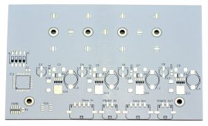
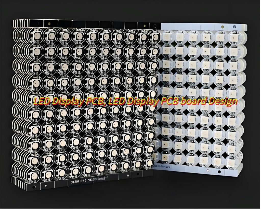
An LED Display PCB is the critical circuit board that connects and controls thousands of LEDs in a screen. It’s a high-performance system engineered to handle power distribution, heat dissipation, and signal integrity. Whether you’re building a curved video wall or an outdoor billboard, the PCB ensures precise color accuracy, brightness uniformity, and long-term reliability.
What Are Components of LED Display PCBs?
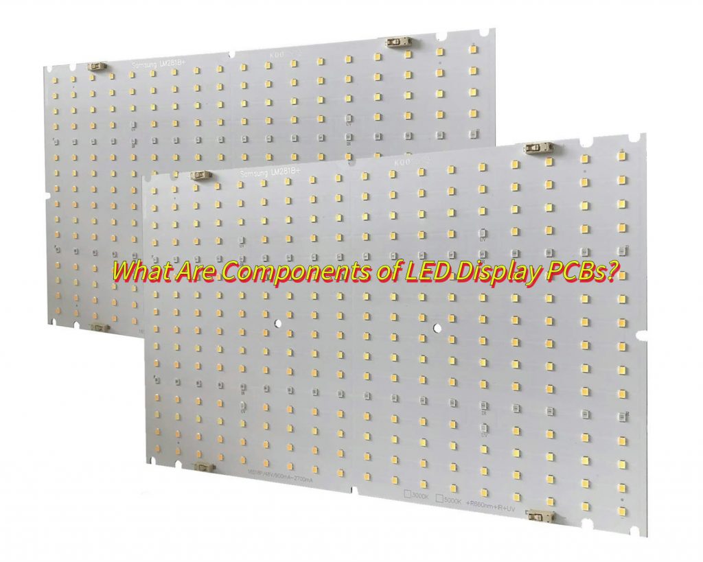
- LED Arrays: Surface-mount (SMD) or chip-on-board (COB) LEDs arranged in grids for pixel-level control.
- Driver Circuits: ICs like MBI5124 or TLC5947 convert data signals into precise current outputs.
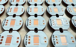
- PCB Substrate: Aluminum core For high-power outdoor screens; FR4 for indoor applications with moderate heat.
- Thermal Management: Heat sinks, thermal vias, and copper layers to prevent overheating.
- Control Interfaces: HDMI, DVI, or Ethernet ports for seamless integration.
What Are Function of LED Display PCB Board?
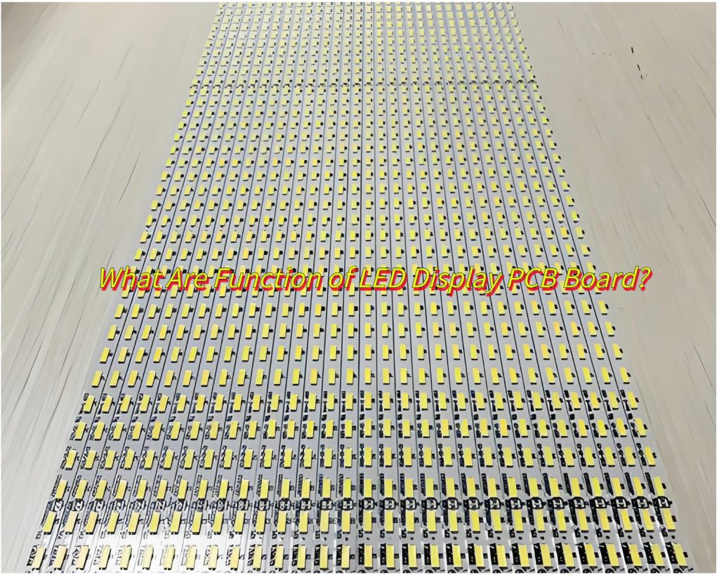
- Structural Support & Component Mounting— Provides rigid base for securing LED beads in precise pixel arrangements and integrates driver ICs, resistors, and other circuitry components.
- Circuit Connectivity & Power Distribution— Copper traces deliver uniform power to all LEDs and transmit control signals to coordinate brightness adjustments and color transitions.
- Thermal Regulation— Aluminum substrates or metal-core designs rapidly dissipate heat from high-intensity LEDs, preventing overheating and ensuring stable operation.
- Signal Conversion & Control— Translates input control signals into executable commands, enabling precise on/off timing, grayscale modulation, and RGB color mixing for each LED.
- System Protection—Incorporates surge protection, short-circuit prevention, and anti-interference designs to enhance reliability in humid/dusty environments.
How Does LED Display PCB Boards Work?
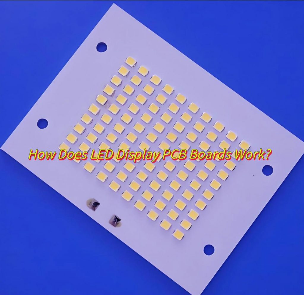
- Signal Processing: Video data is decoded by a controller and split into pixel-specific instructions.
- Current Regulation: Driver ICs adjust current flow to each LED, controlling brightness and color.
- Heat Dissipation: Aluminum substrates or thermal vias channel heat away from sensitive components.
- Output: LEDs emit light at defined intensities, blending colors to create sharp, vibrant images.
How To Design LED Display PCB board?
Here are steps for LED display PCB board design:
1. Pre-Design & Architecture
- Application & Requirements: Prioritize resolution, brightness, and thermal load based on indoor/outdoor use.
- Material Selection: Aluminum-core PCBs for high-power/high-density; FR-4 for low-power/cost-sensitive designs.
- Schematic Framework: Integrate driver ICs (e.g., TLC5940), power regulators, and surge protection.
2. Component Layout
- Position LEDs in strict grid alignment to maintain pixel accuracy.
- Place driver ICs equidistant from LED clusters to minimize signal delay.
- Separate power and control circuitry to reduce EMI interference.
3. Power Distribution
- Implement star topology for power rails to ensure uniform voltage.
- Use thick copper traces (≥2oz) for high-current paths to prevent voltage drop.
4. Signal Routing
- Route clock/data lines as matched-length differential pairs.
- Apply ground planes between signal layers to enhance EMI shielding.
5. Thermal Design
- Incorporate thermal vias under high-power LEDs.
- Allocate 20-30% board area for heat dissipation in high-density layouts.
6. Prototype Testing
- Validate signal integrity with oscilloscope checks for ghosting/crosstalk.
- Measure thermal performance under maximum load conditions.
- Conduct accelerated aging tests for solder joint reliability.
How to Choose LED Display PCB Board Design Service?
The following tips will helps you how to choose LED display PCB board design service:
Technical capability verification:
- Confirm whether the supplier has experience in LED-specific PCB design:
- High-density layout (such as small-pitch LED optimization design).
- Heat dissipation design (aluminum substrate application experience).
- Signal integrity control (long wiring such as CAN/SPI protocol).
Customization support:
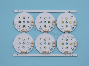
- Special-shaped PCB design (non-standard shapes such as round and curved).
- Function expansion (touch screen, high refresh rate integration).
- Modular compatibility (adaptation to standard installation structure).
Supply chain and cost control:
- Whether to provide full-process services (PCB production, patch, component procurement).
- Low-cost solution capabilities (such as FR-4 substrate selection, mass production optimization).
Best Technology focuses on the full-process service of LED display PCB, integrating high-density layout (supporting small pitch optimization), aluminum substrate heat dissipation and precise signal control to ensure thermal stability and low latency; supporting special-shaped PCB processing, touch screen integration and modular design; relying on self-built factories to achieve one-stop delivery of PCB production, patch and component procurement, and reducing costs by 30%+ through FR-4 substrate and batch process optimization. If you’re interested in our service, please feel free to contact us.( The email is at the beginning of this blog)
Can LED Display PCBs Design Be Customized?
Yes, LED display PCBs design can be customized. Here are customizable options for LED display PCB boards:
- Size/resolution: Adapt to different scenarios (indoor/outdoor), support modular splicing (such as 160mm×160mm standard module).
- Special design: Support irregular shapes such as round and curved surfaces (additional process cost required).
- Function expansion: Integrated touch, high refresh rate, CAN bus and other protocols.
- Material selection: Aluminum substrate for high power, FR-4 for low cost; OSP/metallurgy optional surface process.
How to Design to Reduce LED Display PCB Costs?
Here is two kinds of methods to how to design to reduce LED display PCB costs:
- Material Substitution: Use FR4 + thermal vias instead of aluminum for indoor screens (saves 30%). Driver Flexibility: Design boards compatible with multiple ICs (e.g., ICN2038S, MBI5124) to avoid vendor lock-in.
- Standardized Modules: Pre-tested power and control circuits reduce development time by 40%. Case Study: High-Brightness Stadium Display
Here is a case want to share with you:
Challenge: A client needed a 12,000-nit LED board resistant to extreme heat and vibration.
Our Solution: 4-layer aluminum PCB with embedded copper heat sinks. Optimized driver placement to reduce trace length by 35%. Achieved 50,000+ hours MTBF with zero color degradation.
To sum up, the above content is all about the components and function of LED display PCB, as well as how it works, how to select a design service to reduce costs. If you want to get more information for LED display PCB, please feel free to leave a message below this blog. Looking forward to your message!
Tags: LED Display PCB, LED Display PCB board, LED Display PCB board Design


