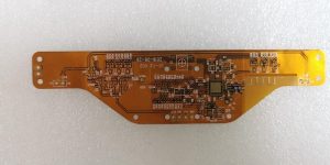
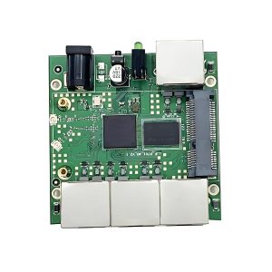
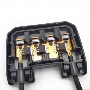
BGA PCB manufacturing has become the go-to choice for compact, high-performance electronics. It’s used widely in smartphones, automotive systems, and industrial equipment. Thanks to its reliability and dense packaging, more engineers now turn to this technology to improve space and performance.
Best Technology is a professional manufacturer specializing in BGA PCB manufacturing and BGA PCB assembly service. We have our SMT factories in China & Vietnam respectively. In China, Best Technology has 2 YAMAHA & 2 JUKI production lines in the SMT factory. The equipment is purchased from Japan. We have 6 SMT lines in Vietnam. Each line has automated PCB loaders. Besides, SMT lines are equipped with the GKG automated solder paste printer, which is the most famous in China. Additionally, Best Technology is equipped with advanced inspection systems such as X-ray, 3D AOI (Automated Optical Inspection), and 3D SPI (Solder Paste Inspection).
These technologies enable us to precisely control the soldering quality and yield rate of BGA PCBs, thereby significantly optimizing overall BGA PCB manufacturing costs for our customers. Have questions about BGA PCB design, BGA PCB prototyping, or BGA PCB assembly? Just let us know at sales@bestpcbs.com, and we’ll handle the rest!
What is BGA in PCB?
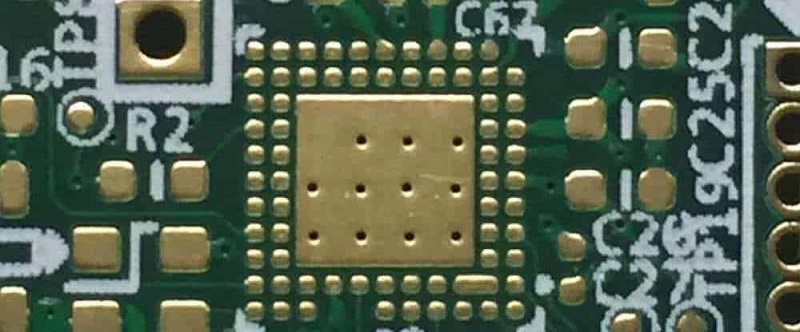
BGA stands for Ball Grid Array. It is a surface-mount package used to mount integrated circuits. In a BGA, solder balls replace traditional pins and sit underneath the component. These balls connect to the PCB during reflow soldering. This layout allows more interconnection points in a small area, boosting both strength and electrical performance.
Compared to older packages like QFP (Quad Flat Package), BGA offers better heat dissipation and signal integrity. It’s a smart fit for high-speed and multi-layer PCBs.
Is BGA an IC?
Not really, BGA is a type of IC package. The actual chip inside could be a processor, memory, or controller. The BGA structure simply defines how it is mounted onto a PCB. What makes it different from other packages is the grid of solder balls instead of leads. This structure not only saves space but also enhances mechanical stability.
What is the BGA PCB layout?
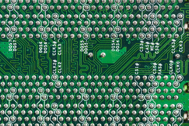
The BGA PCB layout refers to how traces, pads, and vias are arranged to match the solder ball pattern. It requires careful planning. Designers often use HDI (High-Density Interconnect) techniques to create tight routing paths.
Key points in BGA layout:
- Maintain short trace lengths.
- Use via-in-pad or micro-vias when needed.
- Allow thermal relief for heat-sensitive components.
Following strict BGA PCB design guidelines ensures good soldering and electrical performance.
How is a BGA PCB manufactured?
BGA PCB manufacturing starts like most PCB fabrication processes. The steps include:
- Design & CAM processing: Designers create Gerber files with BGA layouts.
- Material cutting & layering: PCB cores and prepregs are prepared.
- Drilling & plating: Vias are drilled and plated with copper.
- Imaging & etching: Circuit patterns are developed.
- Solder mask & silkscreen: Protective layers are applied.
- Surface finish: ENIG is often used for BGA pads.
- Testing & inspection: AOI and flying probe tests ensure quality.
These steps ensure a reliable foundation for the BGA assembly process.
What is the manufacturing process of BGA PCB assembly?
BGA PCB assembly is a delicate and skilled process. Here’s how it works:
- Solder paste printing: Precise paste is applied on each pad.
- BGA placement: A BGA placement machine picks and places the component.
- Reflow soldering: Controlled heat melts the balls, forming joints.
- X-ray inspection: Since joints are hidden, X-ray checks for voids or shorts.
- Final testing: Electrical tests verify function.
Proper reflow profiles and inspection steps are crucial for long-term reliability.
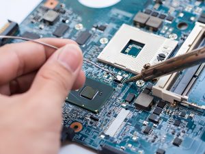
How hard is it to solder BGA?
Soldering BGAs manually is nearly impossible due to their hidden pads. However, automated reflow ovens make the process smooth and repeatable. The key challenges include:
- Maintaining proper heat profiles
- Avoiding voids in solder joints
- Ensuring correct alignment
X-ray inspection after soldering ensures everything is in place. With good equipment and a skilled team, BGA soldering is highly dependable.
How is the BGA PCB manufacturing cost?
BGA PCB manufacturing cost depends on several factors:
- Board complexity: More layers and finer traces increase cost.
- Pad density: High-density designs need advanced capabilities.
- Surface finish: ENIG is more expensive than HASL but better for BGAs.
- Assembly type: Turnkey PCB assembly is more costly but convenient.
- Quantity: Larger runs lower per-unit cost.
Despite the cost, BGA PCBs offer great value due to better performance and miniaturization. Just feel free to let Best Technology know your requirements for BGA PCB manufacturing projects, and we will get back to you with the best BGA PCB manufacturing cost.
What factors affect BGA PCB manufacturing quality?
Several factors impact BGA PCB quality:
- Design accuracy: Good layout reduces defects.
- Material selection: FR4 may be enough, but advanced PCBs may use Rogers or others.
- Fabrication precision: Tight tolerances ensure proper pad alignment.
- Soldering process: Correct profiles avoid bridging or cold joints.
- Inspection tools: X-ray and AOI boost reliability.
Each step from design to inspection plays a role in product quality.
Why Choose Best Technology for BGA PCB Manufacturing?
At Best Technology, we offer end-to-end support for BGA PCB manufacturing. With over 18 years of experience, we handle complex BGA PCB layouts and BGA PCB assemblies with good quality. Our facility features:
- In-house fabrication and assembly: Our vertically integrated facilities include advanced SMT lines, precision laser drilling equipment, and automated optical inspection (AOI) systems. We specialize in high-density BGA PCB manufacturing with impedance control, and offer full turnkey BGA PCB assembly from BGA PCB prototyping to BGA PCB mass production. Rigorous process controls (e.g., nitrogen reflow soldering, 3D SPI for solder paste inspection) ensure defect rates below 2%. All processes comply with IPC Class 3 standards and AS9100D aerospace-grade reliability requirements.
- X-ray inspection and BGA rework stations: We adopt Triple-inspection system, which is AOI, X-ray, Cross-section Analysis. All BGA PCBs undergo 48-hour thermal cycling tests to ensure flawless performance in extreme environments. And we have BGA rework stations for those needing precise repair or component replacement. Our rework stations integrate advanced temperature control and optical alignment systems to ensure accurate reballing or soldering of BGA components, maintaining the original design specifications. Post-rework, all repaired boards undergo reinspection (via X-ray and AOI) to validate integrity, guaranteeing that reworked BGAs meet the same reliability standards as new units
- Full material traceability: Best Technology has MES systems in our SMT factories. We make sure every component is correct and traceable.
- Global shipping and fast lead times: Global shipping and fast lead times: Combined with a strong R&D team, sales engineers, and excellent management personnel with more than 10 years of experience, Best Technology is able to reply to customers within 12 hours wherever you are on Earth and ship out goods 30% faster than other manufacturers in BGA PCB industry. Our lead time policy in 2025 is within 2-3 weeks.
Best Technology supports your engineers and purchasing teams with personalized service. Whether you are launching a new product or scaling production, we are here to help. Just don’t hesitate to reach out to us at sales@bestpcbs.com.
In conclusion, BGA PCB manufacturing has opened new possibilities for compact and high-speed designs. While the process needs precision, it also brings long-term advantages. Choosing the right BGA PCB manufacturing partner ensures that your boards are built to last. At Best Technology, we’re ready to turn your BGA PCB design into reality. For inquiries or custom quotes, reach out to our team at sales@bestpcbs.com!