Best Technology Co.,Ltd
- +86-755-2909-1601
- sales@bestpcbs.com
Military-grade Quality, Trusted Performance
One-stop Customization Solutions
24-hour Sample Response
Professional Team, Technical Support
Professional Customization, Quality Assurance
High Performance Package Solution
Miniaturized Design Solution
Ultra-thin Structure Solution
Classic Stable Solution
High Density Package Solution
High Performance Array Solution
Multi-chip Module Solution
Exclusive Custom Package Solutions
Professional Technology, Quality Assurance
Withstands temperatures above 200℃, strong mechanical shock resistance
High thermal conductivity with low thermal expansion coefficient, effectively reduces thermal stress
HTCC process ensures package hermeticity, prevents moisture intrusion
Supports deep customization, non-standard solutions delivered within 3 weeks
Widely Used in Various High-tech Fields
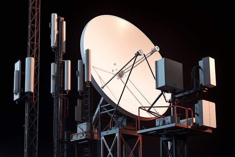
High-frequency Communication Equipment Packaging
Industrial Control Systems

Defense and military industry
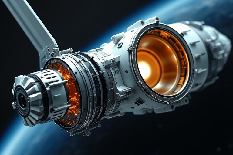
Aviation Electronics Equipment
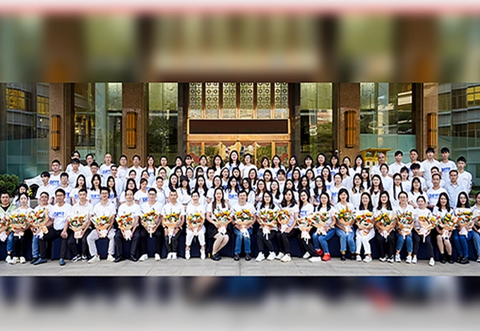
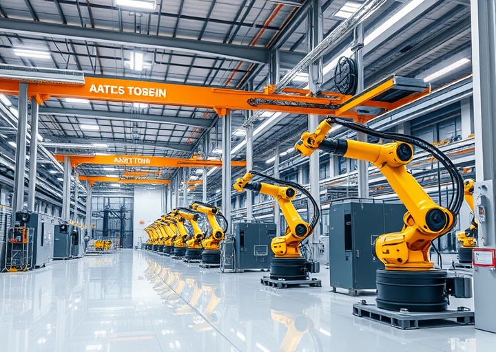
Founded on June 28, 2006, Best Technology is committed to providing one-stop PCB solutions to drive technological advancement and innovation. With over 18 years of experience, we have become a trusted partner for clients worldwide, offering best solutions to meet the growing needs of the electronics industry.
Our products ranging from standard FR4 PCB, multi-layer PCBs, metal-based PCBs (MCPCBs), ceramic PCBs, flexible and rigid-flexible PCBs to high frequency PCBs. Currently our mouthy capability is 260,000 square feet (28,900 square meter), more than 1,000 different boards will be completed. We also provide expediate service, so that urgent boards can be shipped out within 24 hours.
At a custom printed circuit board manufacturer, we believe that continuous growth is the key to success. So, we always invest much in research and development to stay ahead of industry trends. Our focus on product quality and customers satisfaction, and we aim to build strong relationships and offer personalized support and solutions to our customers.

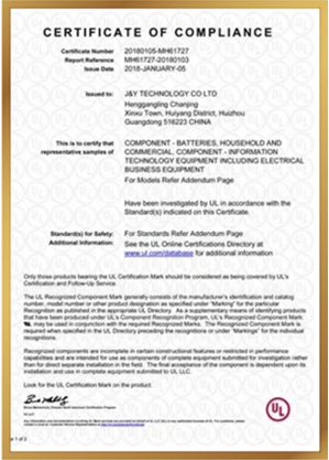
We hold relevant quality certifications that validated our commitment to provide high quality products. These certificationsact as a guarantee of product excellence, ensuring customers and partners a good quality assurance practices.
Professional Team Provides One-stop Solutions
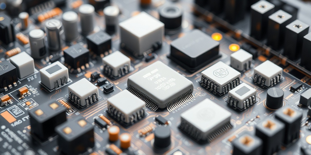
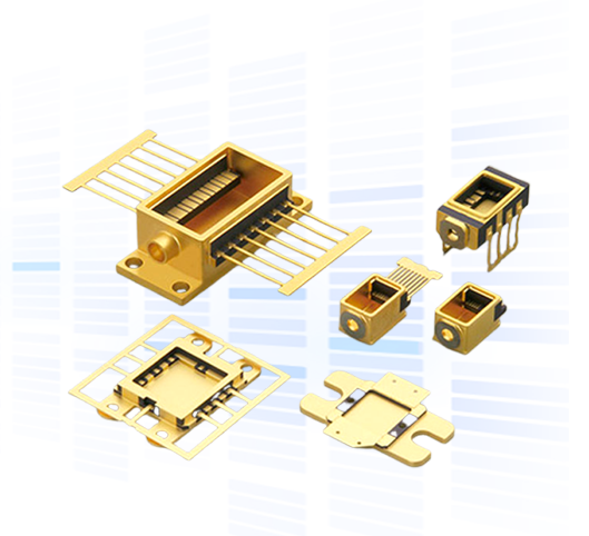
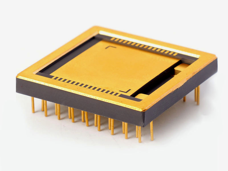
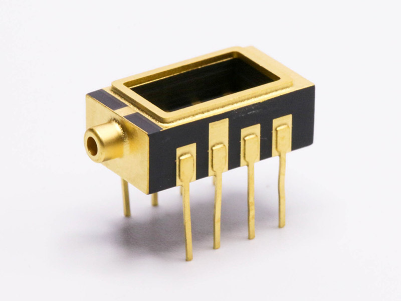
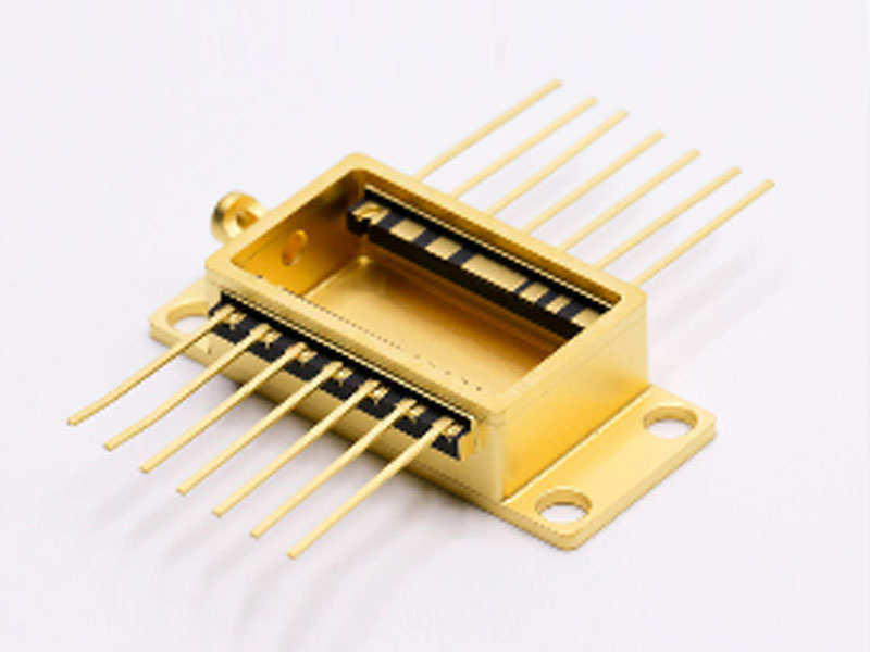
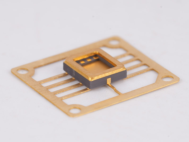
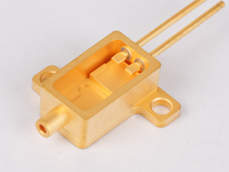
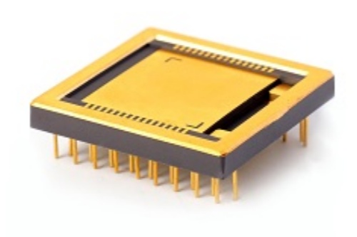
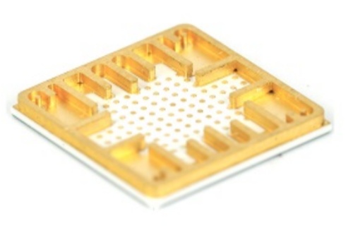
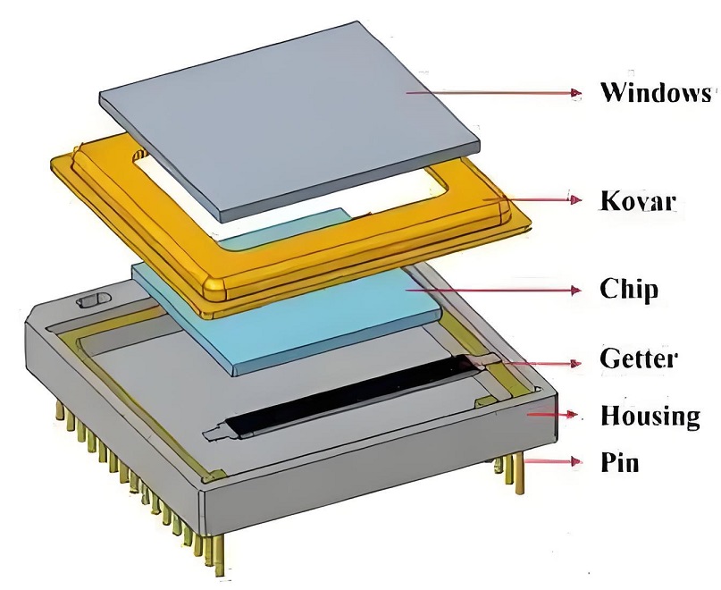
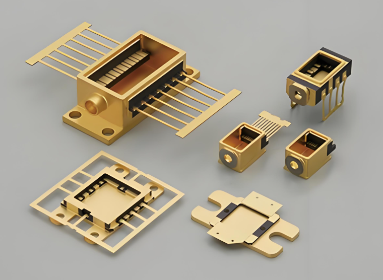
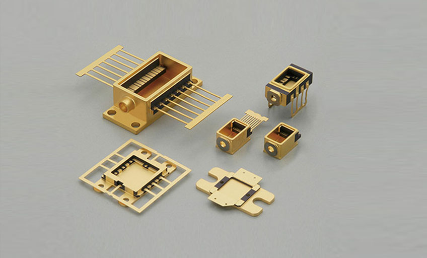
Ceramic package, also known as ceramic packaging housings or ceramic package shell, it is a ceramic material made, heat-resistant protective shell used to protect semiconductors and other microelectronic components. It holds the chip securely, connects it to the outside world, and shields it from damage caused by heat, moisture, or physical stress. Unlike plastic packages, ceramic enclosures can tolerate much harsher environments.
This packaging type is often used in defense, aerospace, and high-performance computing. It’s also common in medical, communication, and automotive fields. As electronics get smaller and more powerful, the need for reliable packaging increases. Ceramic packages meet this demand well because they stay stable over time, even in extreme conditions.
Ceramic packaging begins with carefully selected raw materials. These materials give the package its strength, heat resistance, and reliability. The most common material is alumina (Al₂O₃), a ceramic made from aluminum oxide. It is known for its excellent insulation and mechanical toughness. Alumina is used in most standard ceramic packages due to its cost-effective and good thermal properties.
For applications needing better heat dissipation, beryllium oxide (BeO) and aluminum nitride (AlN) are used. These materials offer better thermal conductivity than alumina, though they are more expensive. BeO material has excellent thermal control but must be handled carefully due to its toxicity when powdered.
Glass frits are added to form seals during manufacturing. These create tight bonds between ceramic layers and keep moisture out. Tungsten, molybdenum, and sometimes platinum are used as metallization materials. They are chosen for their thermal expansion properties, which match well with ceramic materials, reducing the chance of cracking during temperature shifts.
Together, these materials give ceramic packages their long-term performance and structural integrity. Each element is chosen to support high thermal performance and mechanical strength, which is essential for mission-critical electronics.
There are several types of ceramic packages according to different package structures, shapes and used technology, the main types are:
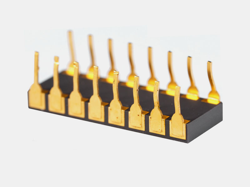
The ceramic dual inline package is one of the oldest types. It has two parallel rows of metal pins, which plug into a socket or PCB. The chip is sealed inside the ceramic body with a metal or glass lid. CERDIPs are known for their robust structure and excellent sealing. Though less common today, they are still used in military and aerospace systems due to their reliability.
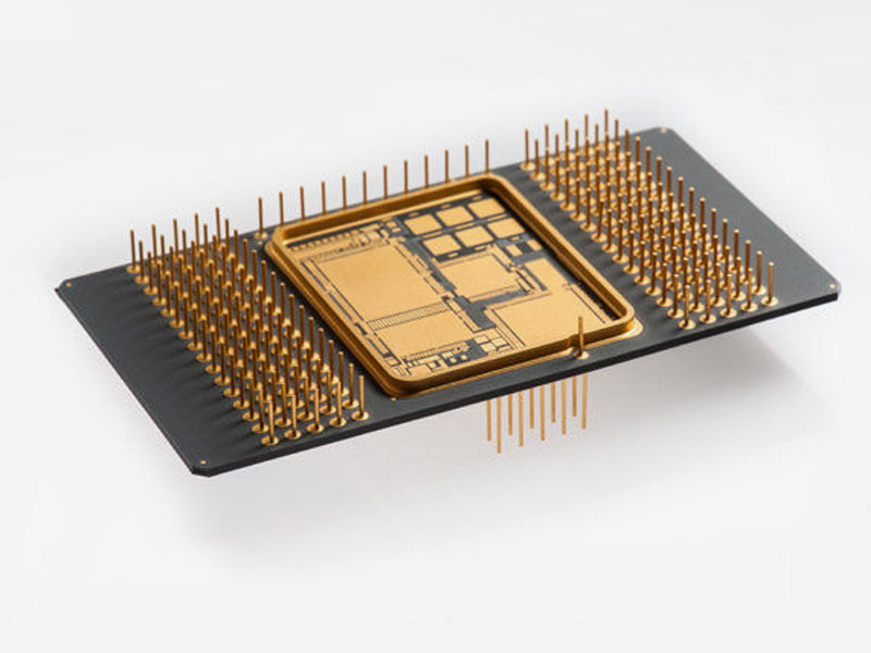
A ceramic IC package is a general term for any ceramic housing that contains an integrated circuit. These packages may be rectangular or square, with flat leads (as in flatpacks), pins (as in pin grid arrays), or solder balls (as in BGAs). Ceramic IC packages are preferred for high-speed and high-frequency devices because they reduce signal loss and interference.
The LTCC package is built using thin layers of ceramic tape. These layers are printed with circuits, stacked, and fired together at a low temperature (around 850°C). This process allows the embedding of passive components like capacitors and resistors directly inside the package. LTCC packages are widely used in RF modules, mobile devices, and satellite systems.
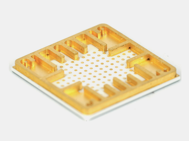
The HTCC package is similar in concept but is fired at a higher temperature (around 1600°C). It uses coarser ceramic particles and usually includes materials like tungsten or molybdenum. HTCC packages are more rugged and can handle harsh environments. They are ideal for power modules, EV applications, and defense electronics.
It also can be classified into several types according to different shapes and structure, the details are including:
Each of these ceramic packages is built for a specific performance range. Choosing the right type depends on your circuit needs, size limits, and the expected operating conditions.
Though both LTCC and HTCC technologies involve co-firing ceramic layers, their differences make each suited for different tasks.
1. Manufacturing Temperature
LTCC is processed below 1000°C, which allows the use of low-resistance metals like silver and gold. HTCC, fired above 1600°C, requires more robust metals like tungsten or molybdenum due to the heat.
2. Circuit Density
LTCC supports more complex multilayer designs. You can integrate filters, inductors, and capacitors directly into the layers. This reduces the need for external components and saves space. HTCC is better for simpler, more rugged designs. It’s stronger mechanically and better suited to large power modules or environments with physical or thermal stress.
3. Cost and Application
LTCC is slightly more expensive due to gold usage and the integration of passive parts. It’s best for telecom, sensors, and RF designs. HTCC, being tougher and often larger, fits power control, aerospace, and defense applications.
Producing a ceramic package involves multiple precise steps, including the ceramic metallization technology. Each stage contributes to the overall reliability and performance of the final product. Below is the complete process from raw tape to finished ceramic package:
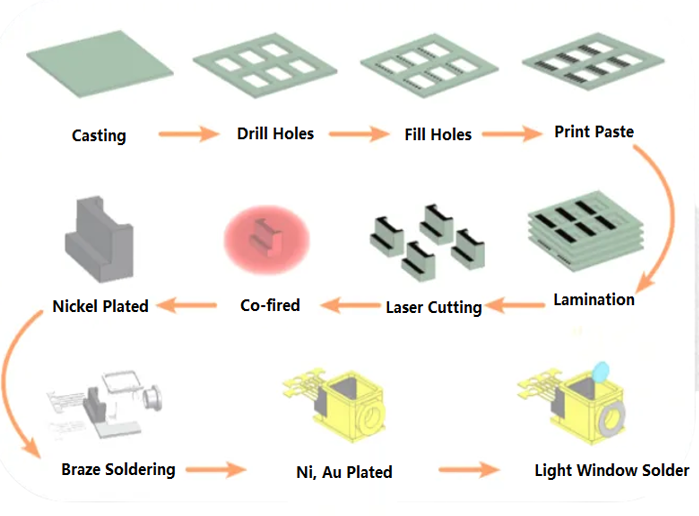
1. Casting
The process starts with casting. A ceramic slurry made from fine powders, binders, and solvents is spread into thin, flexible sheets known as green tapes. These sheets are the foundational layers that will later be stacked to build the ceramic body.
2. Drill Holes
Once the green tape is dry, it goes through mechanical or laser drilling. Tiny holes, called vias, are punched to allow vertical electrical connections between layers.
3. Fill Holes
The drilled vias are then filled with conductive paste—typically made from tungsten, molybdenum, or gold-based materials. This paste forms the internal circuit paths during the firing stage.
4. Print Paste
Next, conductive traces and patterns are screen-printed onto the surface of each ceramic layer. This includes signal lines, ground planes, and pads. At this stage, internal circuit designs begin to take shape.
5. Lamination
The printed ceramic sheets are carefully stacked in the correct order and pressed together under heat and pressure. This lamination step bonds the layers into a single solid block, ensuring tight alignment and structure.
6. Laser Cutting
Before firing, laser cutting is used to define the outline of the final package. It also creates windows or alignment notches if needed for optical or structural purposes.
7. Co-Fired
The laminated block is then co-fired in a high-temperature furnace. For HTCC, the firing temperature is around 1600°C. For LTCC, it’s about 850°C. This sinters the ceramic layers and solidifies the conductive paths. After this stage, the ceramic body is hard, dense, and electrically functional.
8. Nickel Plated
The next step involves plating the exposed pads and via ends with a thin layer of nickel. This forms a barrier layer that prevents oxidation and prepares the surface for future soldering or bonding.
9. Braze Soldering
Any metal parts—like lead frames or metal lids—are attached to the ceramic body using braze soldering. This process uses high-melting-point alloys to ensure a strong, air-tight seal.
10. Ni/Au Plated
To improve solderability and prevent corrosion, the connection areas are further plated with nickel and a final thin layer of gold. Ni/Au finish is reliable and stable, especially for wire bonding or flip-chip mounting.
11. Light Window Solder
In some packages, a transparent window is added—commonly used in optical or sensor modules. This window is soldered onto the ceramic body with precision to ensure optical clarity and a strong mechanical seal.
Ceramic packaging is used where high reliability is critical. Here are some examples:
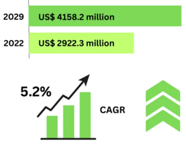
The ceramic packaging market is experiencing significant growth, driven by the increasing demand for reliable and high-performance electronic components across various industries. According to 《Global HTCC Ceramic Substrate Industry Research Report, Growth Trends and Competitive Analysis 2024-2030》from QY Research:
1. The global HTCC ceramic substrate market sales reached 5 billion yuan in 2023 and is expected to reach RMB 8.7 billion in 2030, with a compound annual growth rate (CAGR) of 7.8% (2024-2030).
2. Japan is currently the world’s largest market for HTCC ceramic substrates, with a market share of more than 70%, followed by the Chinese market, with a share of about 20%.
3. HTCC products can be divided into HTCC ceramic substrate, HTCC package shell, HTCC package base. In terms of products, HTCC ceramic housing is the largest market segment with a share of about 75%.
4. In terms of application, HTCC can be used in consumer electronics, communication field, industrial field, automotive electronics, aerospace and military fields, the largest application is consumer electronics, followed by communications.
Key Growth Drivers of Ceramic Package:
When talk about ceramic packages, people always confused it with ceramic PCB. Though both use ceramic materials and offer excellent heat resistance and stability, they serve completely different purposes. One protects the chip inside a sealed enclosure, while the other acts as a printed circuit board carrying and connecting multiple components. Below is a clear comparison to help you understand how these two ceramic-based technologies differ:
| Aspect | Ceramic Package | Ceramic PCB |
| Definition | A sealed enclosure that houses and protects semiconductor chips | A printed circuit board made from ceramic material to mount electronic parts |
| Main Function | Protects the chip and enables external connection via leads or pads | Supports components and provides electrical interconnection |
| Structure | Enclosed, often multi-layer with internal vias and braze-sealed covers | Open board with conductive traces on surface or inside layers |
| Thermal Properties | Excellent heat resistance and dissipation | High thermal conductivity, especially with AlN |
| Moisture Protection | Fully sealed for hermetic protection | Not sealed; moisture resistance depends on surface finish and coating |
| Size and Format | Small and compact; designed for single or multi-chip enclosures | Larger in size; supports multiple passive and active components |
| Mounting Type | Usually used for chip-level mounting onto PCBs or boards | Directly mounts passive and active components |
| Assembly Method | Flip-chip, wire bonding, or braze soldering inside the package | Standard SMT or through-hole soldering |
| Cost | Higher due to sealing, material, and precision manufacturing | Lower to moderate depending on layer count and material |
At Best Technology, we offer full support for ceramic package development. Our experience with ceramic package semiconductors, LTCC and HTCC, and custom design ceramic package solutions gives you the confidence to build high-reliability systems.
We offer:
When precision, performance, and durability matter—choose Best Technology. We’re here to help you innovate with confidence.

With the rapid development of 5G technology, high-performance ceramic packaging is increasingly used in communication equipment. This article analyzes the characteristics of ceramic packaging materials and their key role in 5G communication equipment.
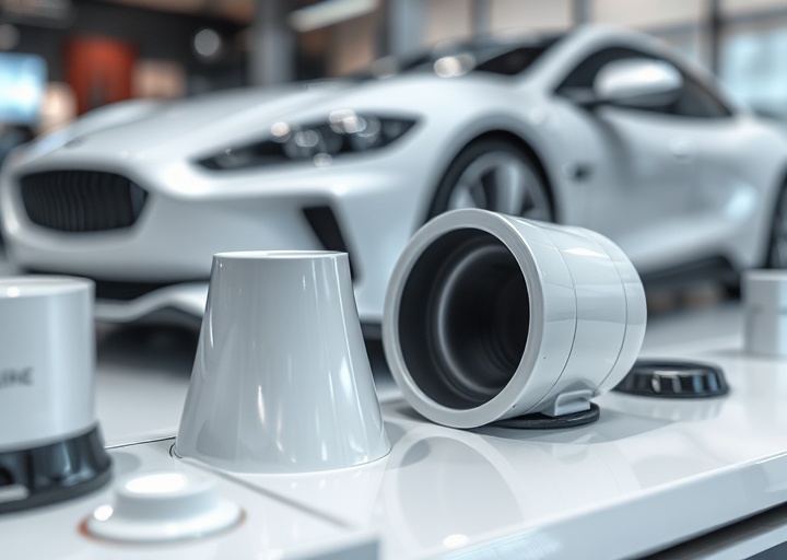
Exploring ceramic packaging applications in new energy vehicles and autonomous driving, analyzing its performance advantages in high-temperature and high-humidity environments.

Introducing breakthrough developments in ceramic packaging materials, including application prospects of innovative materials such as nano-ceramics and composite ceramics.
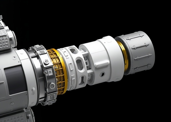
In-depth discussion of ceramic packaging applications in spacecraft, satellite communications, and other high-end fields, focusing on reliability performance in extreme environments.
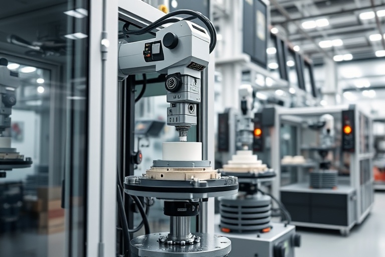
Detailed introduction to the intelligent upgrade of ceramic packaging production lines, exploring innovative applications of AI technology in quality control and process optimization.
Suitable for 5G Communications, Aerospace, and Other High-end Fields
Professional Engineering Team Available 24/7