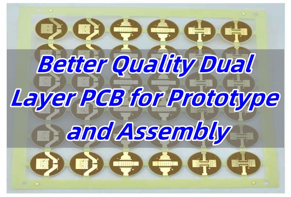
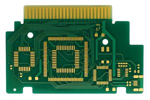
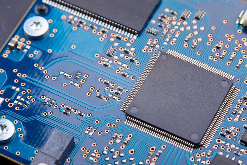
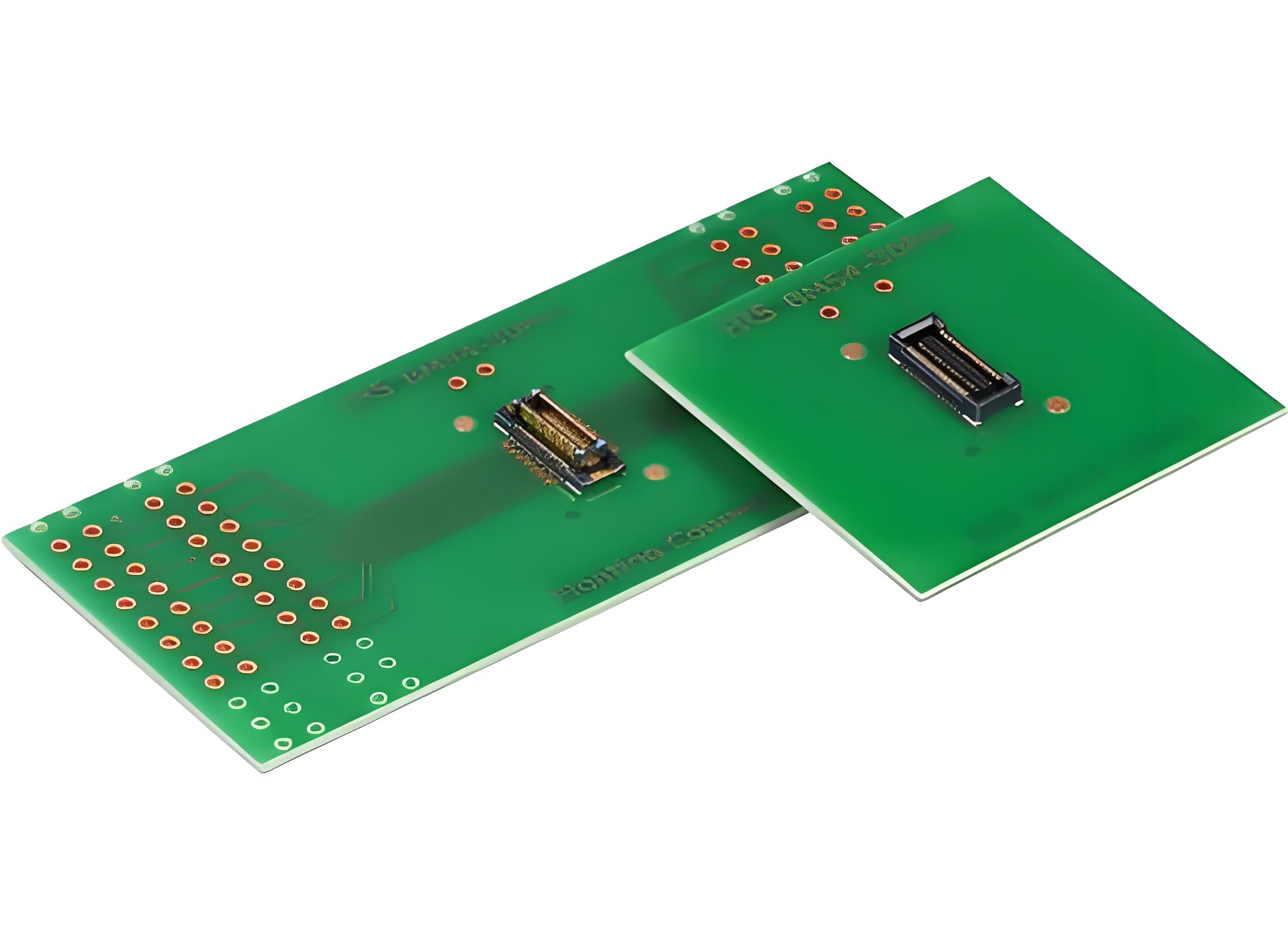
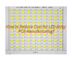
Dual layer PCB is often the top choice when balancing performance, cost, and compact design for both prototype and production. It’s ideal for engineers who need reliability without the complexity of multi-layer designs. In this blog, we’ll explore what it is, how it compares to other PCB types, and how Best Technology helps you overcome real design and manufacturing challenges.
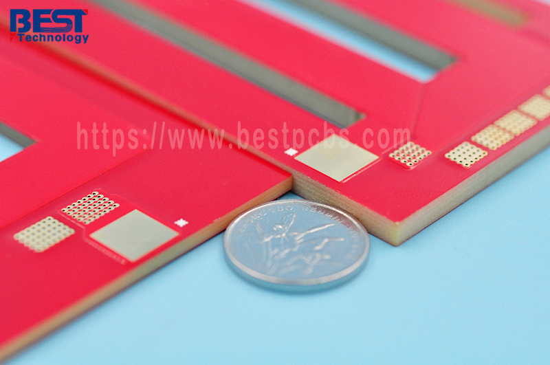
Best Technology is a China EMS PCB manufacturer, presenting better quality dual layer PCB for prototype and assembly service to worldwide clients and markets. Our standard process for double layer PCBs supports a minimum finished board thickness of 0.2mm ±0.1mm, compatible with ENIG surface finish. For special requirements, we can produce boards with thicknesses ranging from 0.15mm to 0.4mm (±0.1mm) within a maximum size of 350×350mm. Our rigid PCB line varies, including heavy copper PCB, extra thin PCB, high Tg PCB, HDI PCB, and RF PCB. For any help, please contact our team by calling +86-755-2909-1601 or email at sales@bestpcbs.com.
What is a Dual Layer PCB?
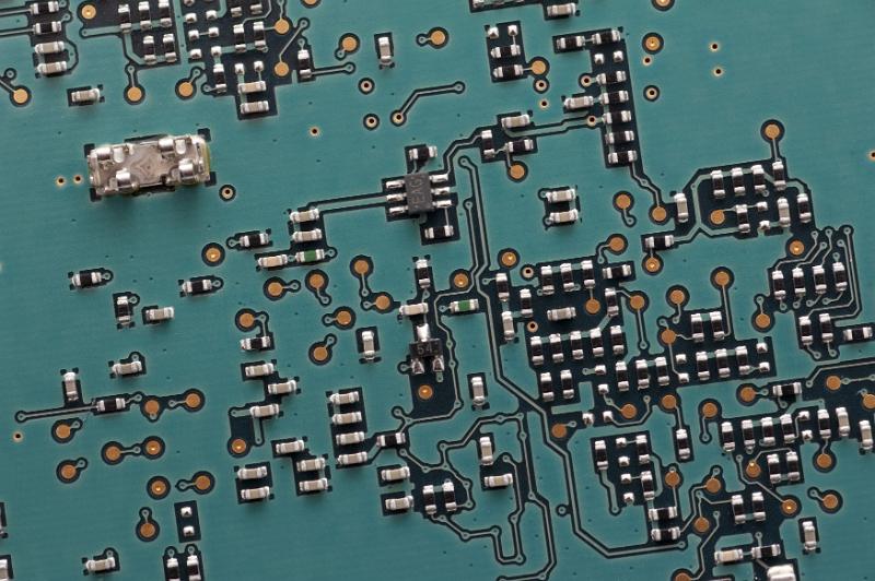
A dual layer PCB, also called a double-sided PCB, has two copper layers—one on the top and another on the bottom. These layers are connected by plated through-holes. This structure allows for denser routing and more components compared to single layer boards. Dual-layer PCBs strike a strong balance between simplicity and capability.
What is the Difference Between Single and Double Layer PCB?
Single layer PCBs have components and routing only on one side. They are simple, low-cost, and easier to produce. But they can be limiting in complex circuits. Dual layer PCBs, by contrast, offer routing on both sides, providing more space and better electrical performance. For example, you can separate power and signal traces better, which improves noise control and makes debugging easier.
What is the Difference Between Dual Layer PCB and 4 Layer PCB?
A dual layer PCB has two copper layers, while a 4-layer PCB includes additional inner layers, usually for power and ground. This extra space gives better EMI shielding and more routing options. But it comes at a higher cost and longer lead time. Unless the circuit requires that added complexity, dual-layer designs are often more practical for cost-sensitive applications.
What are 2-Layer PCB Design Rules?
Effective design helps avoid signal problems and manufacturing defects. For a 2-layer PCB, key rules include:
Route high-speed signals near a ground plane to reduce interference.
Use decoupling capacitors near power pins to stabilize voltage.
Ensure impedance matching for differential pairs like USB or HDMI.
Minimize vias and layer transitions to keep costs low.
Best Technology’s engineers help review your design before production to catch layout issues early. Our team uses automated DRC/DFM tools to prevent costly mistakes.
How Much Does a 2 Layer PCB Cost?
Prices depend on board size, copper thickness, surface finish, and order volume. On average, small batch prototype PCBs start at $30–$80, while larger production runs can bring per-unit cost below $1. At Best Technology, we offer cost control strategies like layout optimization, material selection (such as CEM-3), and bulk ordering for better pricing.
What is a Double Layer PCB Board Used For?
Double layer PCBs are used in a wide range of electronics. Common examples include:
Power supply modules
Lighting systems like LED drivers
Consumer electronics like smart devices
Industrial control boards
Their simplicity makes them easy to test and repair, yet they are robust enough for demanding use cases. With good layout, they can also handle moderate-speed signals and analog circuits.
Where to Get Dual-Layer PCB?
Choosing a reliable partner matters. Best Technology provides dual layer PCB solutions tailored to your needs. We support prototyping, mass production, and turnkey assembly. Every board goes through electrical testing, visual inspection, and X-Ray for via quality. We also solve common pain points faced by engineers:
EMI issues? We suggest layout improvements and material selection to reduce noise.
Signal quality concerns? Our impedance control ensures clean signals for fast communication.
Soldering defects? We use AOI and X-Ray to catch issues before boards ship.
Our MES system ensures every component and batch is traceable—improving quality and simplifying troubleshooting.
In brief, dual layer PCBs are a great choice for prototypes and production alike. They offer a balance of performance and cost. But without proper design and process control, issues like signal loss, EMI, or soldering errors may arise.
Best Technology solves customer needs with complete solutions: from layout optimization, precision drilling, automated assembly, to final testing. Whether you’re in automotive, medical, or consumer products, our team ensures your board meets every requirement. You can contact us at sales@bestpcbs.com, and be sure to give us Gerber files, quantity, and any special requirements so that we can quote you as fast as we can.
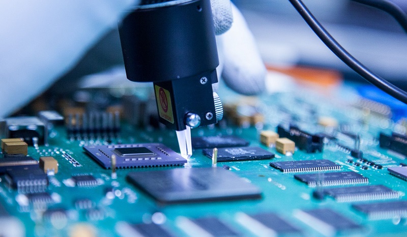
Electronic circuit board parts are essential in every electronic device you use. From your phone to a smart appliance, these parts make it all possible. But beyond their function, how can buyers ensure they’re getting the right parts—on time and with the quality expected?
What Are Electronic Circuit Board Parts and Functions?
Electronic circuit board parts include resistors, capacitors, ICs, transistors, and connectors. Each part plays a role. Resistors control current. Capacitors store charge. ICs manage logic or power. Transistors amplify signals. Connectors allow external communication. When working together, they perform complex operations with precision.
What Are the Printed Circuit Board Components Symbols?
Symbols help identify each component in a circuit board diagram. For example, a resistor is shown as a zigzag or rectangle. Capacitors are two parallel lines. Diodes have arrows. These symbols appear on schematics, making PCB assembly more efficient and avoiding errors.
How to Identify Electronic Circuit Board Parts?
Identification starts with visual inspection. Labels like R1 (resistor), C1 (capacitor), or U1 (IC) help. However, when visuals aren’t enough, using a multimeter or an electronic component identifier app gives accurate readings. You can also refer to circuit board components identification PDF guides for reference.
What Electric Circuit Board Parts Are Valuable?
ICs, power modules, and RF components usually have high value. Older boards may also include gold-plated connectors, making them more valuable for recycling. In modern times, components like microcontrollers, sensors, and programmable chips carry the highest replacement cost and importance.
What Is Electronic Circuit Board Definition?
An electronic circuit board is a structured panel that connects electronic components using conductive pathways, often made from copper. These boards, also called PCBs, are the heart of any electronic system—supporting, connecting, and powering all the individual parts.
What Is the Printed Circuit Board Parts HS Code?
The standard HS code for printed circuit board (assembled) is 853400. Parts for printed circuit boards have various HS codes depending on the specific component type, for example, integrated circuits (HS 8542), capacitors (HS 8532), and resistors (HS 8533). This international code helps customs classify and clear these goods globally. It ensures trade consistency and helps avoid delays at borders.
Where to Get Electronic Circuit Board Parts?
Reliable sourcing is key. That’s where Best Technology comes in. We help companies eliminate common supply chain issues—wrong parts, excess stock, or delivery delays. Best Technology specializes in electronic circuit board manufacturing, and we supply electronic circuit board parts as well. Our MES system enables traceability. Combined with ISO and IATF certifications, we guarantee consistent delivery and performance.
Why Best Technology Is Trusted by Global Brands?
Let’s face it—managing electronic circuit board parts is no simple task. Errors in BOMs, outdated inventory, or sudden spec changes can break a project. Best Technology tackles these headaches directly:
Automated Part Tracking: With smart MES systems, we trace every component through procurement, assembly, and testing.
Flexible Volume: Whether it’s small batches or large volume, we meet tight timelines with reliable results.
Accurate Cost Control: Our digital systems reduce manual errors and our personnel give realistic quotes from the start.
Quality Assurance: We meet ISO 9001, ISO 13485, IATF 16949, AS9100D standards and all our material parts are compliant with UL, REACH, and RoHS.
Supplier Network: We qualify all vendors through strict audits, ensuring stable supply and excellent performance in every lot.
From electronic circuit board parts to SMT PCBA, clients come to us with urgent timelines and complex designs. They stay because we handle component sourcing, DFM analysis, and quality control better than others. Through our flexible coordination and lean manufacturing tools, we provide printed circuit board components and offer a viable EMS turnkey PCB assembly solution.
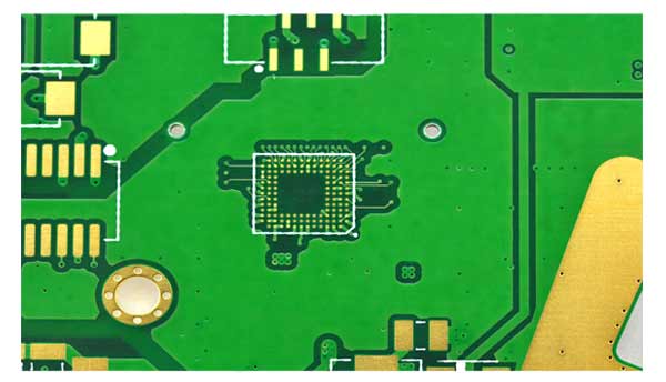
Top down close up view on resistors and other electronic parts on green colored printed circuit board
In closing, Getting electronic circuit board parts shouldn’t feel like solving a puzzle. Whether you’re building power supply units, sensors, or IoT modules, Best Technology offers consistency, smart support, and global reach. No more BOM headaches. No more quality doubts. Just streamlined sourcing and reliable delivery. You can reach Best Technology by email at sales@bestpcbs.com. Partner with Best Technology—where your circuit part, PCB prototype, fabrication, and assembly get the attention they deserve and your projects run on time, every time.
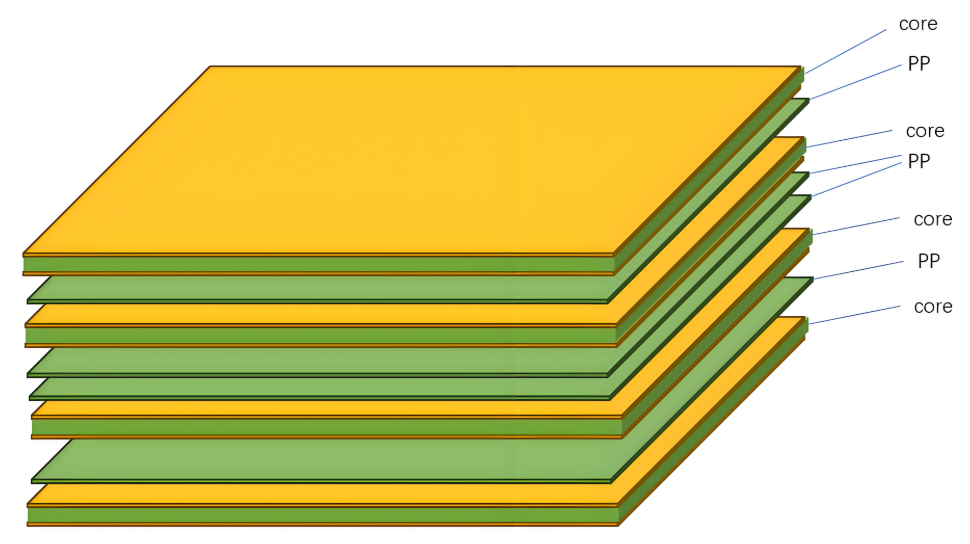
Designing a reliable multilayer circuit board starts with getting the stackup right. If your project involves high-speed signals, compact layouts, or reduced EMI, an 8-layer PCB stackup is a solid choice. It offers flexibility, better performance, and room for complex routing.
In this guide, we’ll walk you through everything you need to know—layer configurations, materials, sizes, and how to make the most of this structure with the help of a trusted PCB manufacturer.
What is a PCB Stackup?
A PCB stackup is the arrangement of copper layers and insulating materials inside a circuit board. These layers are stacked and bonded together using prepreg (resin-impregnated fiberglass) and core materials. The goal is to create a reliable board that supports both mechanical strength and excellent electrical performance.
In simple words, the stackup decides how signal layers, power planes, and ground layers are placed in the board. In high-speed digital designs, this structure plays a big role in signal quality, electromagnetic compatibility (EMC), and overall performance.
For an 8-layer PCB, the stackup consists of eight layers of copper with alternating dielectric materials. These are usually divided into four signal layers and four plane layers, though that can change based on your design needs.
PCB Stackup Considerations
For most PCB designs, there are often competing requirements between electrical performance, manufacturing limitations, cost targets, and system complexity. The final PCB stackup is usually a result of careful trade-offs across these factors. High-speed digital circuits and RF systems commonly rely on multilayer boards for better control and performance. Below are 8 essential principles to consider when designing a reliable stackup:
1. Layer Arrangement
In multilayer PCBs, you’ll typically work with signal layers (S), power planes (P), and ground planes (GND). Power and ground planes are usually solid, unbroken areas that provide low-impedance return paths for signal currents. Signal layers are often positioned between these planes to form symmetrical or asymmetrical stripline structures. The top and bottom layers are mainly used for component placement and limited routing. It’s best to keep traces on these outer layers short to reduce direct radiation and EMI.
2. Defining a Single Power Reference Plane
Decoupling capacitors are vital for maintaining power integrity, and they can only be placed on the outer layers of the PCB. The trace length, pad design, and vias connected to these capacitors greatly affect their effectiveness. To improve decoupling, make these connections short and wide, and minimize via length. For example, in a high-speed digital system, place decoupling capacitors on the top layer, dedicate the second layer to power for the processor, use the third layer for signal routing, and assign the fourth layer as a ground reference.
3. Incorporating Multiple Ground Planes
Using multiple ground planes helps create low-impedance return paths and minimizes common-mode EMI. Ground and power planes should be tightly coupled, and signal layers should also be close to reference planes. Reducing the dielectric thickness between layers improves coupling and enhances performance.
4. Managing Multiple Power Planes
When your design includes more than one power plane, these planes are often split into different voltage regions. If a signal layer is placed next to a multi-region power layer, signal currents may not find clean return paths, leading to noise or EMC issues. For high-speed digital signals, avoid routing traces near split power planes to prevent return current discontinuities.
5. Designing Signal Routing Pairs
When a signal travels from one layer to another, it creates what’s known as a “routing pair.” Ideally, the return current should stay within the same reference plane when switching layers. In practice, however, signals often need to transition between layers. To maintain signal integrity, ensure that return paths are available through stitching vias or decoupling capacitors. Using adjacent layers as routing pairs is a practical and effective strategy.
6. Routing Direction Guidelines
Keep trace directions consistent within each signal layer. At the same time, rotate the routing direction between adjacent signal layers. For instance, use horizontal routing (X-axis) on one layer and vertical routing (Y-axis) on the next. This practice reduces crosstalk and improves signal clarity.
7. Even-Layer Designs is Better
Although odd-layer PCBs may appear cheaper due to fewer materials, they’re more expensive to manufacture. That’s because odd-layer boards require non-standard lamination processes and additional handling steps. These increase the risk of surface damage, incorrect etching, and longer production times. In contrast, even-layer PCBs are more stable, cost-effective, and easier to produce at scale.
8. Budget
Multilayer PCBs are naturally more expensive than single- or double-layer boards. However, they offer significant benefits in functionality, miniaturization, EMI control, and signal integrity. When weighing total cost versus performance, the difference between multilayer and simpler boards may not be as high as expected.
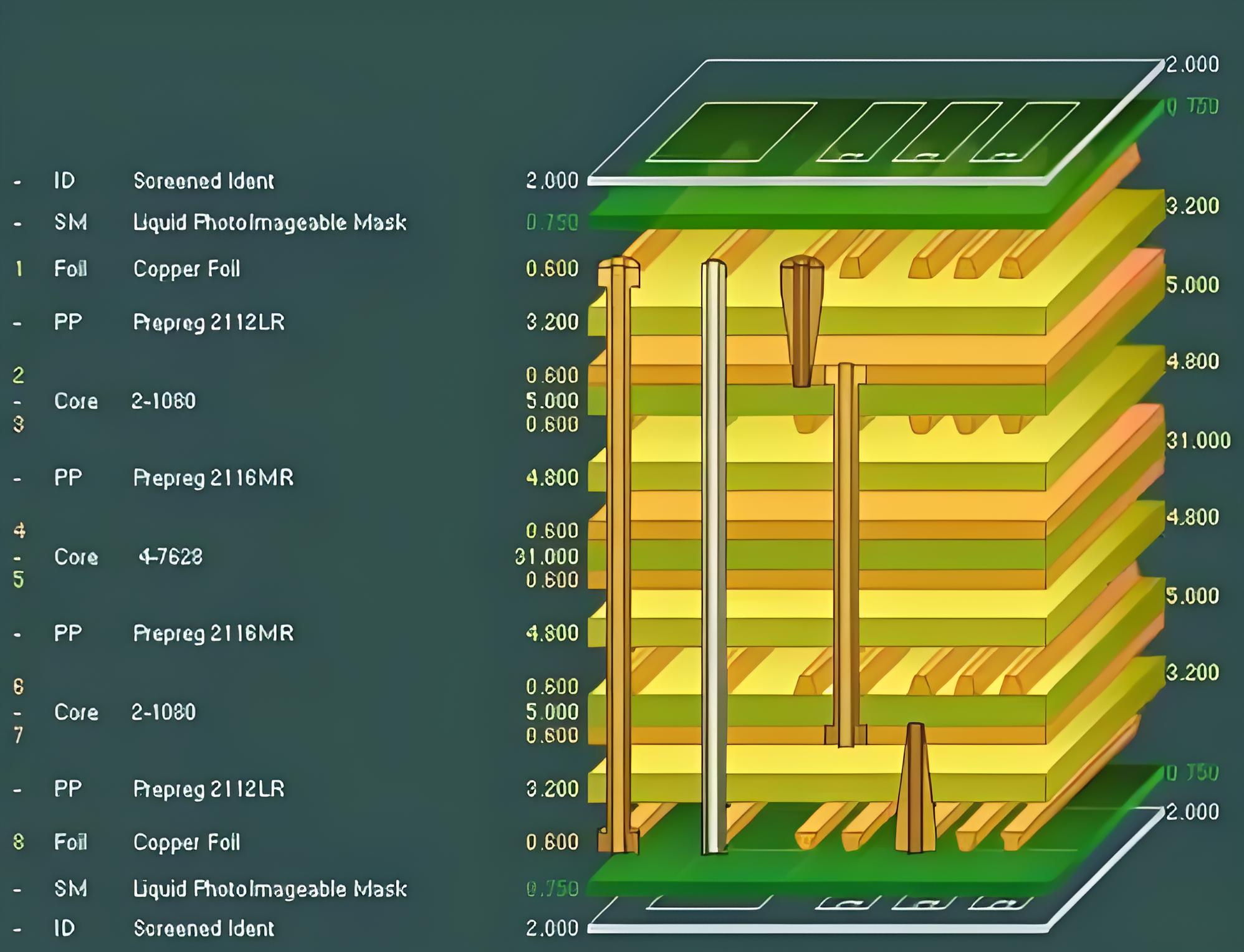
Standard 8-Layer PCB Stackup Structure
When it comes to multilayer PCB design, the arrangement of signal, power, and ground layers directly affects signal integrity, EMI performance, and power delivery. Below are three common 8-layer stackup configurations, each with its own strengths and limitations.
Option 1:
Layer 1: Signal 1
Layer 2: Signal 2
Layer 3: Ground
Layer 4: Signal 3
Layer 5: Signal 4
Layer 6: Power
Layer 7: Signal 5
Layer 8: Signal 6
This layout alternates signal and power layers but does not take full advantage of the electromagnetic shielding benefits that a multilayer board can offer. The ground and power planes are separated, reducing the board’s EMI suppression capability. In addition, the power distribution network suffers from higher impedance, which may affect voltage stability in high-speed or high-current applications.
Option 2:
Layer 1: Signal 1
Layer 2: Ground
Layer 3: Signal 2
Layer 4: Power
Layer 5: Ground
Layer 6: Signal 3
Layer 7: Ground
Layer 8: Signal 4
This structure is widely regarded as the optimal 8-layer PCB stackup. It provides excellent electromagnetic shielding through the use of multiple ground planes. Each signal layer is placed adjacent to a reference plane (either ground or power), which improves signal stability and impedance control. Additionally, the tight coupling between power and ground planes enhances EMI performance and power integrity. This setup is ideal for high-speed, high-frequency, or noise-sensitive applications.
Option 3:
Layer 1: Signal 1
Layer 2: Ground
Layer 3: Signal 2
Layer 4: Power
Layer 5: Ground
Layer 6: Signal 3
Layer 7: Power
Layer 8: Signal 4
This configuration is a variation of Option 1 with improved EMI performance. By adding an extra reference plane, it provides better control over the characteristic impedance of the signal layers. However, the placement of the second power plane (with limited coupling to a nearby ground) leads to higher power delivery impedance, which could be a drawback in power-sensitive designs. Some optimization in power layer arrangement is still needed.
8-Layer PCB Stackup Materials
The performance of an 8-layer PCB stackup relies heavily on the materials used between and around its copper layers. These materials affect everything from electrical behavior to thermal stability and even mechanical strength. Let’s look at the two main categories: conductive and dielectric materials.
1. Conductive Layers
Copper is the most common metal used for the conductive layers in an 8-layer PCB. It’s highly conductive, easy to work with, and available in different thicknesses and finishes.
Copper Thickness: Most boards use ½ oz or 1 oz copper per layer. If the design needs to handle higher current, 2 oz or thicker copper may be used.
Copper Type: Standard copper foil is either electrodeposited (ED) or rolled. Rolled and annealed copper is smoother and more flexible, which makes it useful in boards that need better bend resistance.
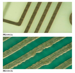
Surface Finishes: The exposed copper is usually treated with a surface finish to protect it and ensure solderability. Options include HASL, ENIG, OSP, and immersion silver, among others.
2. Dielectric Layers
The dielectric materials are the insulating layers that separate the copper traces. These layers are critical for controlling impedance, heat flow, and electrical isolation.
FR-4: A glass-reinforced epoxy laminate, FR-4 is the most common dielectric for general-purpose PCBs. It’s reliable, widely available, and cost-effective.
High-Frequency Materials: For RF and high-speed digital designs, materials with low dielectric loss—like PTFE (Teflon), ceramic-filled PTFE, or hydrocarbon-based ceramics—are preferred. These support better signal integrity at high frequencies.
Thermal Conductive Materials: When heat dissipation is a concern, substrates like alumina or aluminum nitride are used. These materials offer higher thermal conductivity than standard epoxy systems.
To hold everything together, manufacturers use prepregs—uncured fiberglass sheets soaked in resin. Common prepreg materials include FR-4 for standard designs and polyimide for higher thermal or mechanical stress environments.
At the center of the stackup is the core, which acts like a spine for the board. This rigid layer typically uses FR-4 or polyimide, though in some high-power or high-heat applications, metal cores are added to improve thermal performance.
8-Layer PCB Thickness & Sizes
The total thickness of an 8-layer PCB depends on several factors:
Copper thickness: Common values are 0.5oz, 1oz, or 2oz per layer.
Prepreg/Core thickness: Adjusted to achieve specific impedance and board height.
Number of plane vs signal layers: Affects thermal and mechanical behavior.
Common Thickness Options:
1.6mm (0.063″) – Industry standard, suitable for most applications.
2.0mm to 2.4mm – Used when extra copper is needed for higher current.
3.2mm or custom – Selected for industrial or military-grade boards.
PCB Sizes:
Panel sizes are typically 18” x 24” before routing. Your board can be as small as a few millimeters or as large as the full panel, depending on the application.
6 Layer vs 8 Layer PCB
A 6-layer PCB consists of six layers of copper circuitry stacked with insulating layers (prepreg and core) in between. It usually includes:
4 Signal Layers for routing high- and low-speed signals
1 Power Plane to distribute voltage
1 Ground Plane to provide a return path and help with EMI suppression
A typical 6-layer stackup looks like this:
Layer 1: Signal (Top)
Layer 2: Ground
Layer 3: Signal
Layer 4: Signal
Layer 5: Power
Layer 6: Signal (Bottom)
While both 6-layer and 8-layer PCBs are widely used in advanced electronics, they serve slightly different purposes depending on design complexity, signal speed, and EMI requirements. Let’s compare them together:
Aspect
6-Layer PCB
8-Layer PCB
Layer Count
6
8
Typical Configuration
4 signal layers + 1 power + 1 ground
4 signal layers + 2 power + 2 ground
Routing Space
Moderate
More routing room
Signal Integrity
Good, suitable for most mid-speed signals
Excellent, supports very high-speed signal routing
EMI Shielding
Limited shielding with fewer ground planes
Strong EMI control due to multiple ground planes
Power Distribution
Single power plane, higher impedance
Dual power planes, better PDN performance
Design Complexity
Less complex, easier to design and fabricate
More complex, better for advanced designs
Thermal Performance
Adequate for medium power applications
Better heat spreading for high-power components
Cost
Lower fabrication cost
Higher cost due to more layers and materials
Use Case
Mid-level MCUs, general embedded, basic RF
FPGAs, DDR memory, high-speed data buses, complex SoCs
Use a 6-Layer PCB if:
Your design isn’t extremely dense.
The signals don’t require tight EMI control.
You want to balance performance and cost.
There’s no strict need for multiple ground or power planes.
It’s widely used in commercial electronics that don’t involve ultra-high-speed communication or compact multilayer routing challenges.
Choose an 8-Layer PCB when:
High-speed signals (such as PCIe, USB 3.x, DDR4, or SERDES) are involved.
EMI performance is critical, especially in sensitive industrial or medical devices.
You need more space for routing due to a denser component layout.
Stable power delivery is required across multiple voltage domains.
You’re working with a compact form factor that demands vertical signal distribution.
An 8-layer stackup allows designers to pair every signal layer with a nearby ground or power plane, which significantly improves signal quality and reduces noise.
Benefits of Working with an Experienced PCB Manufacturer
Designing and fabricating an 8-layer PCB stackup requires precise engineering and process control. Partnering with a reliable manufacturer like Best Technology brings several benefits:
1. Stackup Design Assistance: Professional help with impedance control, signal integrity, and EMC optimization.
2. Material Expertise: Guidance in choosing suitable laminates for your specific requirements.
3. Advanced Fabrication: Capability to handle HDI, blind/buried vias, and tight tolerances.
4. Quality Assurance: Rigorous testing like AOI, X-ray, and impedance measurement.
5. Fast Turnaround: Efficient production process without sacrificing quality.
Why Choose Best Technology for Your 8-Layer PCB Stackup?
Best Technology is a trusted 8-layer PCB stackup specialist serving global customers across aerospace, medical, automotive, and industrial electronics. We hold certifications including:
ISO9001 for quality control
ISO13485 for medical electronics
IATF16949 for automotive-grade PCBs
AS9100D for aerospace applications
Our engineers assist with DFM check, impedance control, EMI reduction, thermal management, and material choices, ensuring your 8-layer design performs reliably under real-world conditions.
FAQs
1. What is the best layer configuration for an 8-layer PCB stackup?
A balanced configuration like Signal–GND–Signal–Power–GND–Signal–Power–Signal is often preferred for signal integrity and EMI control.
2. How much does an 8-layer PCB cost?
Cost varies by material, size, copper weight, and complexity, but typically ranges from $50 to $300 per board in small batches.
3. What software is used for 8-layer PCB design?
Tools like Altium Designer, Eagle, KiCAD, and OrCAD support multilayer PCB stackup planning and layout.
4. Can you use HDI features in 8-layer PCBs?
Yes. Blind and buried vias, via-in-pad, and microvias are often used in 8-layer HDI designs.
5. How do I choose the right manufacturer for 8-layer PCBs?
Look for certifications, material options, engineering support, and experience with multilayer stackups—like what Best Technology provides.
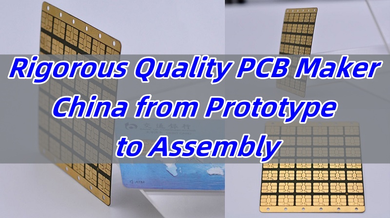
PCB maker China continues to gain global attention for providing complete solutions, from early-stage prototyping to full-scale assembly. Many international buyers look to China for its robust supply chain, flexible production, and lower costs. Yet, concerns around quality, communication, and delivery time often hold them back.
As a trusted PCB manufacturer China, Best Technology caters to professional, responsive, and accurate services that eliminate the most common headaches faced by global customers. Through end-to-end traceability, meticulous quality control service, and 24/7 technical support, we make PCB production efficient, dependable, and stress-free. Some order requirements from some critical industries like the medical and aerospace industries are really strict, but we have the rich experience to tackle them and deliver the integrated solutions to our prospects and regular customers. Best Technology was proven to be in strict compliance with ISO 9001, ISO 13485, IATF 16949, AS9100D, UL, REACH, and RoHS. Please reach out to us via email at sales@bestpcbs.com, and we will be glad to answer any questions you may have.
Who Is the Largest PCB Maker China in the World?
In terms of capacity and revenue, China leads the world in PCB manufacturing. Major players like Zhen Ding Tech, DSBJ, and Shennan Circuits hold dominant market shares and serve massive industries including telecom, automotive, and computing.
While these companies operate at scale, they often focus on large-volume clients. Mid-sized or custom orders sometimes lack the same attention. That’s why many clients turn to companies like Best Technology—where tailored service meets different requests.
Who Manufactures Custom PCB?
Custom PCB production requires more than machines. It needs flexibility, engineering insight, and proactive communication. Many PCB maker China factories offer customization, but only a few deliver it with speed and accuracy.
Best Technology specializes in custom PCBs for industries like medical, automotive, aerospace, and industrial controls. Our team works closely with clients to validate design files, offer DFM feedback, and ensure fast iterations. Whether it’s a 2-layer board or a complex HDI structure, our process is focused on getting it right the first time.
What Services Do Chinese PCB Manufacturers Offer from Prototyping to Assembly?
Top-tier PCB maker China factories provide integrated services to streamline the entire production lifecycle:
Design Support: Help with layout reviews and file conversions.
Component Sourcing: With strict BOM verification.
PCB Fabrication: Single, double, and multilayer boards in FR4, aluminum, or ceramic. Boards made to IPC standards.
SMT and Through-Hole Assembly: Using AOI, SPI, and X-ray for defect detection. Precision placement and temperature-controlled reflow.
Testing: ICT, functional testing, and in-circuit validation.
Box Build: Some even offer enclosure assembly and system integration.
What makes Best Technology different is our end-to-end smart manufacturing system and stringent process control, ensuring zero-defect PCB production from prototyping to mass assembly. We manage everything from prototyping to assembly projects all under one roof.
Is Best Technology Based in China?
Yes. Best Technology is proudly located in Shenzhen, one of China’s major electronics hubs. Our location allows us to access a wide component network, skilled technicians, and responsive logistic services.
Being based in China gives us cost control. But more importantly, it helps us respond fast to changes, reduce lead times, and support complex requirements.
Which PCB Design Software Use Most in PCB Maker China?
Among PCB maker China companies, the most commonly used design tools are:
Altium Designer: Offers powerful 3D layout and rule checks.
PADS: Known for its simple learning curve and wide use.
Cadence Allegro: Preferred for high-speed and dense designs.
Mentor Graphics (Valor NPI): Best for manufacturability verification.
At Best Technology, we work with all mainstream formats. But more importantly, we integrate DFM tools into our front-end process to prevent issues before they occur. This eliminates over 30% of rework and reduces prototype scrap.
Where to Get PCB Manufacturing China List?
Finding a PCB manufacturing China list can be overwhelming. Most lists online mix small trading companies with real factories. To make it easier, Best Technology offers transparency. We are a factory—not a broker. You can visit our facility, view our certifications, and speak directly to engineers. That openness builds trust and eliminates the unknowns.
If you’re comparing suppliers, look for:
Real factory photos and videos.
Certification like ISO 9001, IATF 16949, ISO 13485.
Technical support offerings.
Clear communication channels.
Below is a handpicked list of 5 trusted PCB manufacturers in China that are known for serving both local and global clients across industries.
1. Best Technology
Best Technology offers end-to-end PCB and PCBA solutions, from PCB layout to final assembly. The company solves common customer headaches, such as poor soldering, traceability issues, and delivery delays. Our use of MES systems, vacuum lamination, and intelligent scheduling ensures stable quality and fast turnaround. Best Technology is especially strong in medical, automotive, and high-reliability industrial applications.
2. Fastprint Circuit Tech
Based in Shenzhen, Fastprint is known for its quick-turn prototyping and small-batch production. They provide PCB and assembly services for industries like telecom, automotive, and consumer electronics. Their global logistics support and multi-language customer service make them a top choice for overseas clients.
3. Victory Giant Technology (VGT)
VGT is one of the largest PCB producers in China. They focus on high-volume manufacturing, especially for consumer electronics and mobile devices. Their factories are equipped with advanced production lines and automatic inspection systems for multilayer boards.
4. Kinwong Electronic
Kinwong offers multilayer, HDI, and rigid-flex PCB solutions with a strong reputation for high reliability. They serve the LED, industrial control, and medical device markets. Their quality systems and R&D support set them apart for complex board designs.
5. Shennan Circuits
Shennan Circuits is known for high-end PCB manufacturing, particularly in the areas of servers, base stations, and automotive electronics. Their strength lies in technology innovation, multilayer processing, and international certification compliance such as ISO 9001 and IATF 16949.
Having the right PCB partner in China can save you time, lower risk, and improve product reliability. Whether you’re a startup or a high-volume buyer, this list offers trusted options for your project. If you value stable production, fast delivery, and full traceability, Best Technology is ready to support your goals with professional service and tailored solutions.
Why Choose Best Technology for PCB Maker China?
Best Technology stands out not because we are the biggest, but because we deliver consistent value. Here’s why global clients trust us:
1. Full Process Traceability Using our MES system, we track every production step. From raw materials to final test results, all data is digitally recorded and permanently traceable.
2. Automated Quality Inspection We combine AOI, X-ray, and advanced vision systems to detect defects fast. Problems are fed back to earlier steps, forming a closed-loop quality system.
3. Fast Turnaround Even for Small Orders Many suppliers delay low-volume jobs. We don’t. Our flexible scheduling and predictive planning keep delivery times short, even for prototypes.
4. Professional Communication We know language and time zones matter. Our team includes bilingual engineers, technical translators, and international sales staff trained in cross-cultural communication. We adjust to your time zone for meetings or urgent issues.
5. Strong Technical Support Our engineers review files using Valor NPI and run over 60 DFM checks before production. That means fewer EQs, faster iteration, and better yield.
6. SMT Reliability Our PCBA process is robust against common SMT defects. We fine-tune solder paste usage, component placement, and temperature profiles to avoid solder bridges, tombstoning, and misalignment.
7. Certified and Audited We meet ISO 9001 for general manufacturing, ISO 13485 for medical, and IATF 16949 for automotive sectors. These aren’t just certificates—they reflect our serious attitude toward quality and compliance.
To sum up, choosing a PCB maker China partner isn’t just about cost. It’s about quality, trust, and ease of doing business. Best Technology answers that call by solving the real problems: inconsistent quality, slow deliveries, miscommunication, and technical gaps. We use a real-time MES system, rigorous defect detection process, bilingual support, and DFM tools to bring you fast, reliable results. Whether you’re building a prototype or scaling to volume, our support team stands ready to assist you 24/7. If you or your team would like to pay a visit to our PCB factory, pls reach us via email at sales@bestpcbs.com.
Are you worried about how to choosePCB stacking connectors for your project? This guide explore type selection tips, application, features, stack height for PCB stacking connectors.
How to choose a stacking connector compatible with 5G/6G high-frequency signals?
Why do my stacking connectors frequently fail in a vibration environment?
How to control connector procurement costs under the demand for small batches and multiple varieties?
From design to mass production, can you find a one-stop stacking interconnect solution?
Industrial-grade vibration reinforcement solution: vibration test data sharing (passed 20G/2000 hours test), failure analysis service.
PCBA+SMT service: support 01005 component mounting, realize synchronous thermal management optimization of connectors and PCBs.
One-stop solution: from DFM inspection to mass delivery, 24-hour rapid prototyping, 15-day mass production cycle.
Welcome to contact Best Technology if you have any inquiry for PCBA or SMT service: sales@bestpcbs.com.
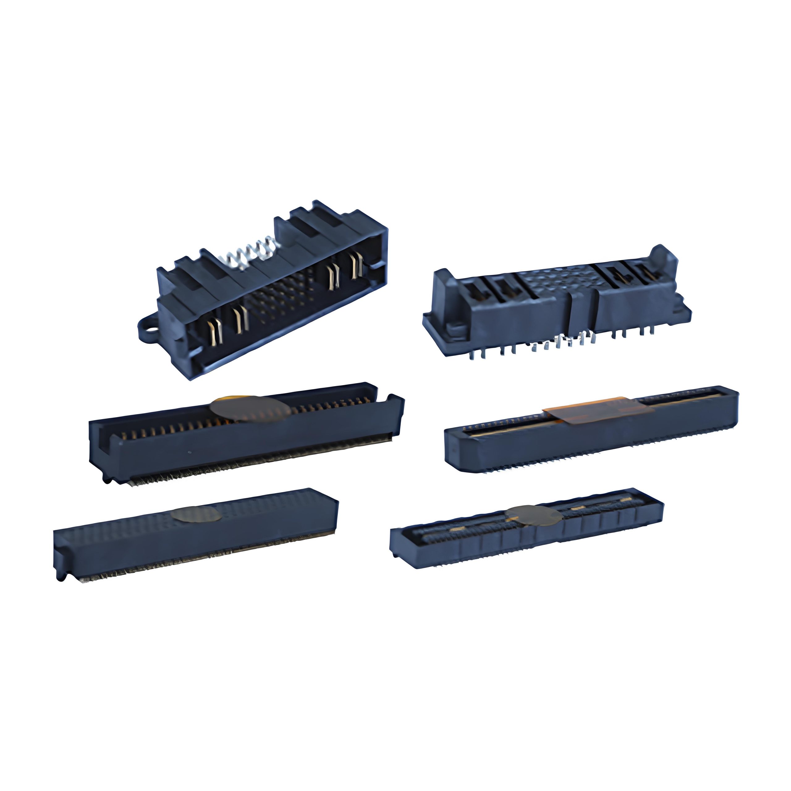
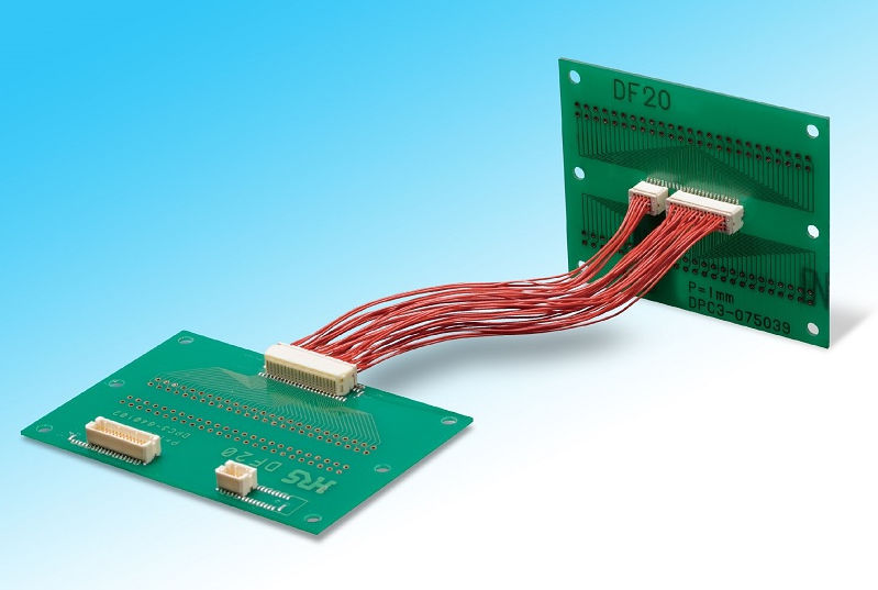
What Are PCB Stacking Connectors?
PCB stacking connectors are specialized interconnect components designed for vertically stacking multiple printed circuit boards (PCBs) to save space in compact electronic devices. They establish electrical pathways between layers while maintaining structural integrity, integrating signal pins for data transfer alongside dedicated power and ground contacts for stable current distribution.
These connectors feature precise alignment mechanisms to ensure reliable mating across stacked layers, often supporting differential pairs for high-speed protocols like PCIe or USB. Their design incorporates impedance-matched layouts to minimize signal reflections and electromagnetic interference (EMI). Mechanical stability is enhanced through locking features that prevent disconnection under vibration, with contact materials selected for durability across temperature variations. Selection depends on parameters such as stacking height adjustability, pin pitch density, and current-carrying capacity.
Application: Used in scenarios requiring bending or dynamic connections, such as foldable devices (e.g., laptop hinges), medical wearables, or robotic joints.
Selection Advice: Prioritize for low-hardness silicone or polyimide substrates to maintain signal integrity after repeated bending. Verify the minimum bending radius to avoid stress-induced damage.
2.Mezzanine Connectors
Application: Suitable for compact stacking designs like single-board computers (SBC), communication base station modules, or vertical interconnections between consumer electronics motherboards and daughterboards.
Selection Advice: Focus on pin density (e.g., 0.5mm/0.8mm pitch) and impedance control. For high-frequency applications, select models with differential pair layouts. Surface-mount (SMT) types are recommended for automated assembly.
3.Board-to-Board Connectors (Vertical/Horizontal)
Application: Vertical types save horizontal space (e.g., IoT modules), while horizontal types suit short-distance connections between parallel boards (e.g., power modules and control boards).
Selection Advice: For vertical connectors, validate insertion/extraction force and durability. For horizontal types, ensure pin pitch and creepage distance comply with high-voltage safety standards.
3.Coaxial Stacking Connectors
Application: Designed for RF or microwave signal transmission in 5G communication devices, radar systems, or satellite communication modules.
Selection Advice: Choose 50Ω or 75Ω impedance-matched models. Evaluate insertion loss and return loss parameters. Ensure outer conductor grounding aligns with PCB ground plane design.
4.High-Current Stacking Connectors
Application: Used in power distribution networks (PDN) for electric vehicle battery management systems (BMS), industrial motor controls, or high-power LED driver boards.
Selection Advice: Assess per-pin current capacity (e.g., >10A/pin). Select copper alloy materials with silver plating. Consider thermal management paths and supplement with thermal interface materials if necessary.
5.Low-Profile Stacking Connectors
Application: Perfect for ultra-thin devices (e.g., smartphones, tablets) or space-constrained stacking scenarios.
Selection Advice: Prioritize ZIF (Zero Insertion Force) or LIF (Low Insertion Force) designs. Select models with a height below 1.5mm. Verify pin coplanarity tolerance to avoid soldering defects.
4.Hermetic Stacking Connectors
Application: Suitable for extreme environments (e.g., aerospace, deep-sea exploration) or applications requiring air/water-tight protection.
Selection Advice: Use glass-to-metal seal (GTMS) or ceramic packaging. Validate certifications like IP68 or MIL-STD-810. Ensure sealing materials are compatible with operational temperature ranges.
5. Modular Stacking Connectors
Application: Ideal for scalable systems like test/measurement equipment, configurable industrial controllers, or educational experiment platforms.
Selection Advice: Choose modular interfaces supporting hot-swapping. Focus on programmable pin definitions. Reserve redundant pins for future functional upgrades.
6.Optical Stacking Connectors
Application: Used for high-speed optical signal transmission in data center optical modules, fiber communication devices, or LiDAR systems.
Selection Advice: Select MPO/MTP multi-fiber connectors or expanded beam designs. Evaluate insertion loss and return loss. Ensure alignment accuracy and dust-proof protection.
7.Low-Profile Stacking Connectors
Application: Perfect for ultra-thin devices (e.g., smartphones, tablets) or space-constrained stacking scenarios.
Selection Advice: Prioritize ZIF (Zero Insertion Force) or LIF (Low Insertion Force) designs. Select models with a height below 1.5mm. Verify pin coplanarity tolerance to avoid soldering defects.
8.Hermetic Stacking Connectors
Application: Suitable for extreme environments (e.g., aerospace, deep-sea exploration) or applications requiring air/water-tight protection.
Selection Advice: Use glass-to-metal seal (GTMS) or ceramic packaging. Validate certifications like IP68 or MIL-STD-810. Ensure sealing materials are compatible with operational temperature ranges.
9.Modular Stacking Connectors
Application: Ideal for scalable systems like test/measurement equipment, configurable industrial controllers, or educational experiment platforms.
Selection Advice: Choose modular interfaces supporting hot-swapping. Focus on programmable pin definitions. Reserve redundant pins for future functional upgrades.
10. Optical Stacking Connectors
Application: Used for high-speed optical signal transmission in data center optical modules, fiber communication devices, or LiDAR systems.
Selection Advice: Select MPO/MTP multi-fiber connectors or expanded beam designs. Evaluate insertion loss and return loss. Ensure alignment accuracy and dust-proof protection.
What Are Features of PCB Stacking Connectors?
Features of PCB Stacking Connectors:
Space-saving design: Allows tight board stacking for compact devices.
High-speed support: Maintains signal integrity for PCIe/USB with impedance control.
Power management: Dedicated power/ground pins ensure stable current flow.
Mechanical reliability: Locking mechanisms prevent disconnection from vibration.
Adjustable heights: Custom spacing options for thermal/routing needs.
EMI protection: Shielding elements reduce interference in noisy environments.
Application of PCB Stack Connectors
Consumer Electronics – Smartphone display-to-mainboard links, wearable device circuit stacking, laptop power distribution network.
Telecommunications – 5G base station RF module connections, network switch backplane interfaces, satellite communication phased arrays.
Industrial Automation – Robotics control system stacking, CNC machine signal transmission paths, power converter module interconnects.
Automotive Systems – ADAS sensor cluster integration, EV battery management circuits, and infotainment system PCB assemblies.
Medical Technology – Portable imaging equipment module stacking, patient monitoring signal routing, surgical instrument control interfaces.
Aerospace & Defense – Avionics system ruggedized connections, radar array signal distribution networks, satellite payload module configurations.
What Is the Stack Height of Board-to-Board Connectors?
Stack height ranges for board-to-board connectors:
Standard Stack Height Options
Ultra-Low Profile: 1.00–1.50 mm (0.039–0.059 inches) for space-constrained designs like wearables.
Common Range: 3.00–8.00 mm (0.118–0.315 inches) suits consumer electronics and industrial controls.
Extended Heights: 10.00–31.90 mm (0.394–1.255 inches) for modular systems requiring thermal or mechanical clearance.
Precision Increments
Fine adjustments in 0.13 mm (0.005 inch) steps enable exact PCB alignment.
Modular designs offer 1.00 mm (0.039 inch) incremental options between 5.00–16.00 mm.
Application-Specific Guidelines
High-Density PCBs: ≤5.00 mm heights with 0.4–0.8 mm pitch connectors optimize signal integrity.
Vibration-Prone Systems: ≥6.00 mm heights improve mechanical stability.
Power Modules: ≥10.00 mm heights accommodate heat dissipation.
Industry Standards
Stack heights correlate with connector pitch (e.g., 0.8 mm pitch pairs with 5–16 mm heights).
MIL-STD compliance ensures vibration resistance for critical environments.
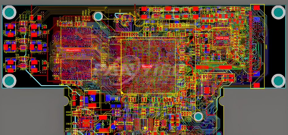
How to Align PCB Stack Connector Precisely in High Density Multilayer PCB Boards?
Precision Alignment Techniques for PCB Stack Connectors in High-Density Multilayer Boards
How to Align PCB Stack Connector Precisely in High Density Multilayer PCB Boards?
Here’s a practical guide for precise stack connector alignment in high-density multilayer PCBs:
Design Phase Preparation
Use identical reference points on all layers (0.1mm diameter).
PCB manufacturer in China isn’t just a phrase—it’s what global companies search for when reliability, scale, and customization matter. Whether you’re working on small-batch prototypes or preparing for volume production, finding the right partner can make or break your timeline and budget.
Best Technology is a PCB Manufacturer in China from Prototype to Assembly. We believe that turnkey EMS PCB manufacturing, no MOQ, high-mix, and shorter lead times are the way to hold our competitive edge. Our factory is compliant with ISO 9001, ISO 13485, IATF 16949, and AS9100D. We have the capability to maintain the quality consistency from PCB prototype to assembly, and provide tailored solutions to automobile electronic PCB manufacturing and medical equipment PCB assembly projects. If you have any questions or any quote requests, please contact us via call at +86-755-2909-1601 or email at sales@bestpcbs.com. We will gladly help.
Who is the Best PCB Manufacturer in China?
Choosing the best PCB manufacturer in China depends on consistency, communication, and the ability to deliver quality boards under tight schedules. What separates an ordinary supplier from the best is not just equipment, but how well they manage orders from quoting to shipping. Best Technology stands out for its integrated MES system, which keeps every process traceable and aligned with your needs. With real-time updates and prompt engineer feedback, customers always stay informed.
We offer a variety of high-mix PCB options to meet your specific needs, including extra-thin PCB, heavy copper PCB, HDI PCB, high-frequency PCB, and high-speed boards, etc. We integrate the entire process from procurement, and mass production through to inspection, reducing your communication time while lowering overall expenses. Our end-to-end Solutions have given us a significant competitive edge in terms of AI smart products, medical equipment, and IOT projects. We will stick to our strengths in terms of quick prototyping to excellent quality assembly and provide full PCB solutions to you.
Who is the Largest PCB Manufacturer in China?
The largest PCB manufacturers in China are known for their vast scale and overseas expansion, such as Wus Printed Circuits Co., Ltd. (WUS), Shennan Circuits Co., Ltd. (SCC), Kinwong Electronic Co., Ltd. However, size isn’t always the measure of suitability. While top players manage millions of square meters per year, mid-sized specialists like Best Technology offer a rare balance—flexibility with industrial-grade infrastructure. We maintain high-speed capacity, making even complex batch changes seamless.
What are the Top 10 PCB Manufacturers in China 2025?
In 2025, China’s PCB industry continues to lead globally in both innovation and production volume. While many manufacturers specialize in specific sectors like HDI, IC substrates, or automotive boards, the top players share one thing in common: strong R&D investment, scalable production lines, and a commitment to international quality standards. Below is a list of the Top 10 PCB manufacturers in China in 2025, based on market size, global influence, technical strength, and customer reputation.
1. Best Technology Co., Ltd.
Best Technology focuses on small to mid-batch custom PCBs, HDI boards, and turnkey PCBA services. Known for flexible scheduling, quick prototyping (24-hour turnaround), advanced inspection systems, and full supply chain integration, Best Technology is a preferred partner for companies needing fast, reliable, and cost-effective one-stop solutions.
2. Shennan Circuits Co., Ltd. (SCC)
Shennan Circuits is well-known for its advanced manufacturing of IC substrates, HDI boards, and flexible PCBs. They are a supplier to top-tier clients in aerospace, telecom, and medical sectors, with a high level of vertical integration.
3. Kinwong Electronic Co., Ltd.
Kinwong offers a full range of PCB solutions, including rigid, flex, and aluminum PCBs. They serve the automotive, industrial control, and lighting markets, and their advanced production lines support large orders with reliable lead times.
4. Victory Giant Technology (Shenzhen) Co., Ltd.
Victory Giant focuses on high-density, multi-layer PCBs and is a leading supplier in consumer electronics. Their strength lies in quick-turn production and steady investment in new manufacturing technologies.
5. Suntak Technology Co., Ltd.
Suntak produces a wide variety of PCB types, including HDI, automotive, and consumer PCBs. They are known for cost-effective solutions and high production yield, serving both domestic and international markets.
6. Aoshikang Technology Co., Ltd.
Aoshikang has made a name in telecom and industrial applications with high-reliability boards. They have strong partnerships with OEMs and focus heavily on automation to ensure consistent quality.
7. Founder PCB (Shenzhen) Co., Ltd.
Founder PCB is backed by Founder Group and specializes in multilayer, high-speed, and HDI PCBs. They have international customers in Europe, the U.S., and Southeast Asia, with robust internal quality systems.
8. Fastprint Circuit Tech Co., Ltd.
Fastprint is well-positioned in the high-mix, low-volume PCB market. They focus on R&D, prototypes, and quick-turn services for clients in medical and industrial sectors, offering full DFM and DFT support.
9. Bomin Electronics Co., Ltd.
Bomin serves the aerospace, defense, and medical fields with high-reliability boards. Their production facilities meet global certifications like AS9100D and ISO 13485, making them a trusted partner for critical applications.
10. Wus Printed Circuits Co., Ltd. (WUS)
WUS is one of the largest PCB makers in China, with a strong presence in server, communication, and automotive applications. They specialize in multi-layer and high-frequency PCBs, with a strong R&D foundation and large-scale production capabilities.
While the PCB market in China remains highly competitive, these top 10 manufacturers lead the way with innovation, capacity, and service excellence. From high-volume powerhouses like WUS and Shennan Circuits to agile and customizable service providers like Best Technology, customers can choose based on their unique project scale and technical needs. If your priority is fast turnaround, cost control, and flexibility—especially for small batches and customized designs—Best Technology offers unmatched advantages with full-stack PCB and PCBA services.
Who are the Top PCB Manufacturers in China Specializing in HDI?
For HDI PCBs, precision matters more than scale. Manufacturers like Best Technology are pushing the edge by combining automated drilling, advanced DFM review, and strict control of blind/buried vias. Our customers benefit from a defect rate below 1%, even for high-layer count boards. With X-ray and strict QC, we detect issues that standard AOI might miss—particularly helpful for applications in 5G and AI-driven products.
Where to Get Custom PCB Manufacturers in China?
Finding custom PCB manufacturers in China means looking for teams who listen, respond fast, and adjust to your requirements. At Best Technology, customization is built into our workflow. From flexible pricing based on batch size to DFM analysis in early design stages, everything we do supports tailor-made success. We even offer BOM risk alerts and material replacement plans to keep your line running smoothly. If any offers about the PCB fabrication, prototype, or assembly, please email us at sales@bestpcbs.com.
How to Choose the Right PCB Maker in China from Prototype to Assembly?
Start by asking: Can they prototype in 24 hours? Can they handle SMT and full box-build? Will they delay delivery due to component shortages? Best Technology answers all with a yes. Our flexible scheduling aligns capacity with order priority. For customers, this means shorter lead times and quick product switches without loss in efficiency. Plus, our self-built component library reduces sourcing delays and supports zero-inventory strategies.
Why Choose Best Technology for PCB Manufacturer in China?
Let’s talk about real customer needs. Today’s demand isn’t about just getting the PCB made in China, which is about getting them fast, flawless, and with less stress.
Planning & Flexibility: With traditional batch models becoming outdated, Best Technology introduces flexible scheduling. Whether it’s 10 units or 10,000, we adapt instantly. Our standard prototyping is under 24 hours, while turnkey PCBA deliveries arrive in just 1–2 weeks.
Quality Assurance: More than 200 control points are inspected using AOI, X-ray, and QC personnel. These layers work together to ensure each product matches the design without invisible faults. SMT lines have real-time sensors that adjust automatically if a deviation occurs, while our DFM check prevents design errors early on.
Integrated Supply Chain: Managing PCB, assembly, and sourcing separately is time-consuming. Best Technology simplifies it all. We collaborate with top vendors to ensure timely supply. Our procurement cycle is as short as 1–3 days, which significantly cuts down your waiting time.
Cost & Risk Management: While raw material and labor costs are rising, we use zero-inventory planning to reduce warehousing costs for clients. BOM lifecycle tracking and substitution alerts help avoid last-minute shortages, reducing rework and overhead.
Tech Upgrade Capability: For industries moving into 5G and AI, Best Technology delivers high-speed, high-frequency, and IC substrate solutions with 99%+ yield. These boards require precise layer alignment, and we manage that using enhanced process control and a trained R&D team.
Talent & Teamwork: Unlike factories that struggle with engineering gaps, we’ve built a solid team of technical experts, always ready to answer, tweak designs, or troubleshoot fast. This helps speed up delivery and ensures stronger product quality from start to finish.
As a final remark, when it comes to working with a PCB manufacturer in China, choosing the biggest isn’t always choosing the best. Customers today want responsiveness, accuracy, and smooth end-to-end service. Best Technology answers those needs with a complete one-stop platform, powered by intelligent systems and expert people. We reduce your headaches from sourcing to delivery while offering full transparency, stronger control, and consistent quality. Do you need the PCB made in China? Whether you’re starting with a single prototype or preparing for full-volume production, contact Best Technology at sales@bestpcbs.com.
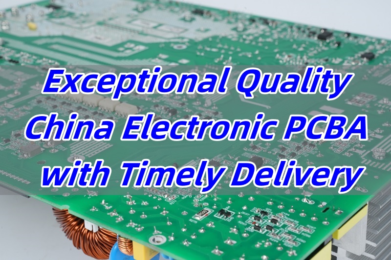
China electronic PCBA is trusted worldwide for its blend of cost-efficiency, advanced production, and skilled engineering. But for many buyers, quality issues and delivery delays remain major concerns. That’s where Best Technology steps in to change the experience.
To sum up, delivering exceptional quality, no MOQ, high mix, on-time delivery, and 24/7 customer service provides us with a competitive edge in the market. If you have new inquiries or any doubts, welcome to call us at +86-755-2909-1601 or contact us at sales@bestpcbs.com. Our customer support team will answer the issues we are receiving as soon as we can, and I’m sure you’ll hear from us soon!
What’s the Meaning of China Electronic PCBA?
PCBA meaning refers to Printed Circuit Board Assembly, which includes both the bare PCB and all mounted components. In short, it’s the final assembled board ready to be used in electronic devices. China electronic PCBA highlights how this complete process is done within China, combining local component sourcing, labor, and advanced production systems to deliver cost-effective and reliable solutions. Many China PCB manufacturers now offer full PCBA services to meet growing demands from international markets.
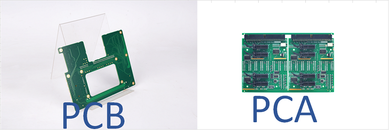
PCBA vs PCB: What’s the Difference?
One of the most common questions is PCBA vs PCB. A PCB is a bare board with copper traces, while a PCBA includes all the soldered parts. This difference matters because many buyers confuse the two. At Best Technology, we support customers from bare board fabrication to full PCBA assembly, including testing, packaging, and traceability. Understanding this helps prevent errors when ordering or quoting projects.
Who Are the Top 10 PCB Manufacturers in China?
Choosing the right PCB partner in China can be difficult due to the sheer number of suppliers. While some focus on mass production, others specialize in high-reliability or high-mix orders. Here’s a quick look at 10 of the top PCB manufacturers in China, known for quality, technology, and scale.
1. Best Technology
Best Technology stands out by offering one-stop PCB and PCBA services with MES traceability, vacuum lamination, and a 3–5 day delivery cycle. We focus on quality-critical industries like medical, automotive, and industrial, and help customers solve problems like soldering defects, traceability gaps, and delivery delays.
2. Suntech Circuits
Suntech is recognized for its ability to handle complex and high-layer-count PCBs. They offer fast prototyping services and export to Europe and North America. Their core strength lies in their technical engineering and reliability.
3. Victory Giant Technology (VGT)
Victory Giant focuses on large-scale PCB production and is known for mass manufacturing of consumer electronics boards. They’ve invested heavily in automation and intelligent manufacturing systems.
4. Wus Printed Circuit
Wus Printed Circuit serves major global brands, especially in the server and storage device sectors. They are one of the oldest PCB manufacturers in China and focus on high-layer and HDI boards.
Fastprint is known for offering PCB and PCBA services under one roof. They focus on quick-turn, small-batch, and high-precision boards, with a strong presence in medical and industrial electronics.
6. Kingboard Holdings
While Kingboard is widely known for its laminate production, it also runs a robust PCB division. It mainly supports consumer and industrial PCBs and is highly integrated across the supply chain.
7. Kinwong Electronic
Kinwong specializes in high-reliability PCBs and is widely used in LED, medical, and automotive applications. Their vertical integration and focus on multilayer boards make them a trusted choice.
8. Shennan Circuits
Shennan Circuits is a well-established player, especially in communication and automotive electronics. The company provides advanced HDI, rigid-flex, and multilayer PCBs with global certifications like ISO 9001 and IATF 16949.
9. Bomin Electronics
Bomin focuses on double-sided and multilayer PCBs for communication and industrial electronics. They are known for steady growth and attention to technical detail in production.
10. Jiangsu Huadong Electronics
Huadong Electronics serves both domestic and international customers. It specializes in rigid PCBs and offers tailored manufacturing to meet specific project needs.
Each of these PCB manufacturers brings unique strengths, from mass production capabilities to customized engineering support. However, if you are looking for a partner who solves real-world needs — like traceability gaps, delayed delivery, or poor communication — Best Technology offers not just manufacturing, but seamless solutions. We help global customers achieve consistent quality and on-time results, no matter how complex the order.
How Does China Lead in PCBA Production with Chinese Electronic Parts?
Chinese electronic parts have become globally competitive due to strong supply chain systems. Paired with advanced process control and highly skilled labor, China electronic manufacturers are meeting increasing international quality standards. At Best Technology, we work with over 2000 verified suppliers and maintain strategic stock of critical parts. This allows us to reduce procurement time by 60% and improve delivery reliability across all orders.
Where to Get PCB Prototype China?
Quick prototyping is key for many electronics projects. For those searching PCB prototype China or China PCBs, Best Technology offers rapid services with 3–5 day turnarounds. Our in-house production system handles PCB fabrication, component sourcing, SMT, and final assembly with traceability. By using a China PCB manufacturer that also provides PCBA, clients reduce communication friction and lead times.
How to Select a Reliable PCBA Manufacturer in China?
Finding a trustworthy PCBA manufacturer in China can be challenging. Many buyers suffer from hidden quality issues like soldering defects, cold joints, or BGA voids. These problems not only affect performance but also increase repair costs. Best Technology solves this with smart production systems: vacuum lamination, BGA ovens with intelligent temp control, and 100% AOI/X-ray inspection. Our MES system ties each board to a unique barcode, making it possible to trace issues within 10 seconds. That’s how we stop issues before they escalate.
Why Choose Best Technology for China Electronic PCBA?
Best Technology is more than just a China electronic PCBA provider. We offer a complete ecosystem to support stable production and prompt delivery. Here’s what makes us different:
1. Quality-first mindset: With IPC-A-610 standards and over 99.95% BGA soldering yield, our factory minimizes rework and increases stability.
2. Full traceability: Every board is tracked via MES. If there’s ever a problem, we locate it fast and fix it early—saving you time and cost.
3. On-time delivery: With flexible scheduling and inventory buffers, we maintain a 97% on-time delivery rate—even for urgent or high-mix orders.
4. Responsive support: We respond to change requests within 24 hours. Our team is always ready to adjust to your needs, reducing stress and avoiding surprises.
5. One-stop service: From PCB layout to SMT to final testing, we simplify your supply chain and reduce vendor management time.
Many customers have faced rising rework costs due to unclear process controls or weak inspection methods. Others struggled with late deliveries caused by poor planning or long component lead times. At Best Technology, we prevent both. Our engineering team handles DFM analysis, adjusts production plans with advanced tools, and stocks critical parts for emergencies. So, you get not only your boards on time but also fewer issues to deal with after delivery.
To conclude, China electronic PCBA services are evolving fast. With increasing pressure on quality and delivery, working with a partner who understands your needs is more important than ever. Best Technology offers a human approach: stable production, traceable quality, and real communication. Our tools, processes, and people are built to deliver end-to-end solutions. If you have any questions about your project, let us know via email at sales@bestpcbs.com. We will take care of it for you.
Why choose MCPCB for LEDapplications? This guide explores metal core PCB specifications, material comparisons (copper vs aluminum), advanced heat dissipation techniques, and practical design solutions for optimal LED performance.
“Insufficient heat dissipation of high-power LEDs leads to accelerated light decay and substandard product lifespan?”
“The processing cost of aluminum substrates is low, but the unstable welding yield affects mass production efficiency?”
“The traditional MCPCB is heavy, which limits the design of lightweight lamps?”
Best Technology Can Provide
The copper-based MCPCB (thermal conductivity of more than 380W/mK) is used with a high thermal conductivity insulation layer to ensure that the core temperature is 15-20℃ lower than that of the aluminum substrate, extending the LED life by more than 30%.
Patented surface treatment technology (such as enhanced OSP+ laser etching) achieves zero oxidation of the pad, and the SMT yield is increased to 99.2%, which is compatible with the full process of reflow soldering/wave soldering.
Ultra-thin aluminum substrate (0.8mm thickness) + hollow structure design reduces weight by 40% while maintaining heat dissipation performance, and has been successfully applied to compact scenes such as downlights or car lights.
Welcome to contact us if you have any request for MCPCB: sales@bestpcbs.com.
What Is MCPCB for LED?
A MCPCB for LEDis a specialized thermal management solution that efficiently dissipates heat from high-power LED components. The board features a layered construction with a metal base (typically aluminum), a thermally conductive dielectric layer, and copper circuitry.
This design allows rapid heat transfer away from LED chips, maintaining optimal operating temperatures and preventing premature failure. The metal core’s high thermal conductivity (5-10 times better than standard PCBs) ensures stable light output and color consistency in demanding applications like automotive lighting, street lamps, and architectural illumination.
By reducing thermal resistance between LEDs and heatsinks, MCPCBs extend product lifespan while enabling more compact, high-density LED array designs. Their structural integrity also minimizes thermal expansion issues during temperature fluctuations.
MCPCB for LED Specification
Here are the technical specifications for MCPCBs used in LED applications:
Base Material Properties
Thickness: 0.8mm to 3.0mm
Thermal conductivity: 1-400 W/mK
Aluminum alloys: 5052, 6061 (typical)
Copper purity: ≥99.9% for copper cores
Dielectric Layer Characteristics
Thickness: 50-150μm
Dielectric strength: 2-6kV
Thermal resistance: 0.3-1.5°C-in²/W
Copper Circuit Specifications
Foil thickness: 1oz (35μm) to 4oz (140μm)
Minimum line width: 0.1mm
Minimum spacing: 0.1mm
Surface finishes: HASL, ENIG, OSP
Thermal Performance Metrics
Junction-to-board thermal resistance: 0.5-3.0°C/W
Maximum operating temperature: 130-150°C
Coefficient of thermal expansion: 20-24 ppm/°C
Mechanical Specifications
Bend strength: 25-40N/mm²
Flatness tolerance: ≤0.15mm/100mm
Hole size capability: 0.3mm minimum
Electrical Properties
Breakdown voltage: ≥2kV
Insulation resistance: ≥10⁸Ω
Dielectric constant: 3.5-5.0 @1MHz
LED-Specific Parameters
SMD pad dimensions: matching standard packages
Solder mask reflectance: 85-92% (white)
Thermal pad coverage: ≥80% of LED footprint
Environmental Compliance
Operating temperature range: -40°C to +150°C
Storage temperature range: -55°C to +155°C
Relative humidity: 5-95% non-condensing
What Is Use of MCPCB for LED Light?
Here are the primary uses of MCPCB for LED lighting:
Heat dissipation – Transfers heat 8x faster than standard FR4 PCBs to prevent LED performance degradation.
Here’s a structured comparison between copper and aluminum MCPCBs for LED lighting applications:
Thermal Performance
Copper: Superior thermal conductivity (~380–400 W/mK), ideal for high-power LEDs or dense arrays where heat buildup is a concern.
Aluminum: Moderate thermal conductivity (~150–200 W/mK), suitable for medium-power applications with adequate airflow.
Cost Efficiency
Copper: 30–50% more expensive due to material costs and machining complexity.
Aluminum: Budget-friendly with acceptable performance for most commercial LED products.
Weight and Mechanical Properties
Copper: Heavier (3× aluminum), which may limit use in weight-sensitive applications (e.g., automotive, portable devices).
Aluminum: Lightweight and easier to machine, enabling faster production and simpler handling.
Thermal Expansion Compatibility
Copper: Closer CTE (17 ppm/°C) to LED chips (6–8 ppm/°C), reducing solder joint stress during thermal cycling.
Aluminum: Higher CTE (23 ppm/°C) may require careful design to avoid long-term reliability issues.
Corrosion and Durability
Copper: Prone to oxidation without surface treatments (e.g., ENIG, HASL).
Aluminum: Naturally corrosion-resistant due to oxide layer formation.
Electrical Conductivity
Copper: Better current distribution for complex circuits or high-current designs.
Aluminum: Requires thicker traces to match copper’s conductivity but sufficient for standard LED layouts.
Manufacturing and Design Flexibility
Copper: Demands specialized equipment for drilling/routing, increasing lead time and cost.
Aluminum: Easier to process, supporting rapid prototyping and cost-effective mass production.
MCPCB Heat Dissipation Solution in High-Power LED Light
Here are practical high-efficiency thermal solutions for MCPCB in high-power LED applications:
Multi-Layer Copper Cladding: Deploying 2-4oz copper foil layers (70-280μm) with optimized trace patterns to enhance lateral heat spreading across the board surface.
Ceramic-Enhanced Dielectric: Using aluminum nitride (AlN) or boron nitride filled dielectric layers (5-20W/mK) to improve vertical heat transfer from LEDs to metal core.
Micro-Channel Embedded Cooling: Integrating sub-millimeter fluid channels within aluminum cores for active liquid cooling in extreme power density applications.
Thermal Via Arrays: Implementing high-density copper-plated through-holes (0.3-1mm diameter) beneath LED pads to create direct thermal pathways.
Phase Change Materials: Incorporating paraffin-based PCM layers (melting point 50-80°C) to absorb and redistribute transient thermal loads.
Graphene-Coated Interfaces: Applying few-layer graphene coatings (500-1500W/mK) at critical junctions to reduce interfacial thermal resistance.
Topological Optimization: Applying generative design algorithms to create organic-shaped aluminum cores that maximize surface-area-to-volume ratio.
How to Design MCPCB Layout and Routing for Optimal Performance?
Here are practical MCPCB layout and routing strategies for optimal thermal and electrical performance in high-power LED applications:
Thermal-Centric Component Placement: Position high-power LED components directly above the thickest metal core sections, maintaining minimum 3mm clearance from board edges to prevent thermal boundary effects.
Symmetrical Power Distribution: Implement star-topology routing for power traces with equal-length branches to ensure uniform current distribution across parallel LED strings.
Copper Thickness Optimization: Use 2-4oz copper layers for current-carrying traces, with wider traces (minimum 2mm width per 1A) to reduce resistive heating and improve heat spreading.
Thermal Relief Patterns: Design circular thermal relief cutouts (0.5-1mm radius) around mounting holes to prevent heat accumulation while maintaining mechanical stability.
Dielectric Layer Configuration: Select dielectric materials (3-8W/mK thermal conductivity) with thicknesses (75-150μm) that balance electrical isolation and thermal transfer requirements.
Dynamic Current Balancing: Incorporate current mirror circuits with thermal-compensated resistors near LED clusters to maintain stable operation across temperature variations.
Examples of Metal Core PCB Heat Dissipation Solutions
Five Common Metal Core PCB (MCPCB) Heat Dissipation Solutions with Verified Data
1. High-Power LED Street Lighting
Application: Municipal outdoor lighting systems using 100W+ LED modules.
Challenge: Prolonged operation at elevated temperatures caused lumen degradation and shortened lifespan.
Solution: Copper-based MCPCBs with embedded thermal vias and a 2mm thick core. The copper substrate directly bonded to the LED array, while aluminum heat sinks attached to the PCB backside enhanced convective cooling.
Result: Junction temperature reduced by 40% (from 110°C to 66°C), extending operational life to 50,000+ hours (verified via accelerated aging tests).
2. Automotive Headlamp Assemblies
Application: LED headlights in compact vehicles requiring minimal space.
Challenge: High thermal density in confined enclosures led to thermal runaway risks.
Solution: Aluminum MCPCBs with a 1.6mm thickness, featuring a serpentine copper trace layout to distribute heat evenly. A graphite thermal pad bridged the PCB and housing, leveraging the vehicle’s airflow for passive cooling.
Result: Stable LED performance at 85°C ambient, with no measurable color shift (Δu’v’ < 0.005) over 10,000 hours (confirmed by spectrophotometer analysis).
3. Industrial UV Curing Systems
Application: UV LED arrays used in printing and coating processes.
Solution: Copper MCPCBs with a 3.2mm core and diamond-coated solder masks for durability. A phase-change thermal interface material (TIM) ensured optimal contact with liquid-cooled cold plates.
Result: Thermal resistance lowered to 0.5°C/W (from 1.2°C/W in baseline designs), enabling continuous operation at 95% power without degradation (validated via thermal imaging and bond strength tests).
4. Industrial UV Curing Systems
Application: Multi-spectrum LED panels for indoor farming.
Solution: Aluminum MCPCBs with a staggered via pattern and copper-filled thermal zones. The boards integrated with passive aluminum fins and active fans for hybrid cooling.
Result: Uniform temperature distribution across the panel (±3°C variance), with a 30% increase in photosynthetic photon flux density (PPFD) efficiency (measured via quantum sensor arrays).
5. Consumer Electronics Flash Modules
Application: High-intensity LED flashes in smartphones and cameras.
Challenge: Rapid heat buildup during short bursts caused user discomfort and component stress.
Solution: Ultra-thin (0.8mm) copper MCPCBs with vapor chamber integration. The vapor chamber spread heat laterally, while ceramic-filled silicone gaskets insulated adjacent components.
Result: Peak temperature during flash activation reduced by 25°C (from 85°C to 60°C), enabling 50% faster repeat firing without thermal throttling (confirmed via infrared thermography and cycle testing).
Instant Quote
This guide covers MCPCB essentials for LED from material selection (copper vs. aluminum) to thermal design and layout optimization. Whether you need high-power heat dissipation or cost-effective solutions, proper MCPCB engineering ensures LED longevity and performance. For precise cost estimation and technical solutions tailored to your LED project requirements, contact Best Technology for professional consultation and quotation service:sales@bestpcbs.com.
China medical PCBA is a critical part of today’s healthcare electronics, where precision and quality directly affect patient safety. Best Technology understands this responsibility. Our team is focused on delivering medical PCBAs that meet strict quality, delivery, and compliance standards.
Best Technology offers great quality China medical PCBA with reliable delivery services in an increasingly competitive market. Manufacturing medical PCBA requires strict quality control, specialized materials, flexible volume support, prompt professional technical support, and regulatory certifications, and the payoff is probably going to be satisfying as it enables medical PCBA innovations while ensuring long-term market competitiveness. To ensure precision, our SMT factory uses state-of-the-art equipment and advanced SMT technology. Our SMT workshop has achieved a 97% on-time delivery rate. If you have any questions or would like to visit our PCBA factory, please email us at sales@bestpcbs.com.
What Is China Medical PCBA?
Medical PCBA refers to printed circuit board assemblies used in medical-grade equipment. These boards control everything from portable monitors to surgical systems. In China, manufacturers like Best Technology produce these assemblies under high-level quality standards. From design support to final testing, each step must follow strict processes. What makes medical PCBAs unique is the level of cleanliness, biocompatibility, and traceability required.
What Certifications Are Required for China Medical PCBA Manufacturers?
Certifications are the gatekeepers of trust in this industry. A top-tier Chinese medical PCBA manufacturer should hold ISO 13485 for medical quality systems. Additionally, compliance with FDA 21 CFR 820, RoHS, and REACH is essential. Best Technology’s production facilities meet ISO Class 7 cleanliness standards. We also maintain AS9100D, ISO 9001, and IATF 16949 certifications — supporting not only healthcare but also aerospace and automotive sectors.
Which China PCB Manufacturer Offers Medical PCBA Manufacturing Services?
Among many names, Best Technology stands out due to our comprehensive service coverage. From the first stage of component sourcing to final functional testing, we manage everything internally. Unlike suppliers who depend on outsourcing, we build your PCBA in a controlled environment with full traceability. We use SPI, 3D AOI, and X-ray inspection to minimize defects.
In What Medical Applications Are LED PCBA Commonly Utilized?
LED PCBA plays a growing role in medical lighting, surgical lamps, and diagnostic tools. Their ability to offer controlled brightness and color accuracy helps improve visibility and accuracy in procedures. In dental lamps, operating rooms, and imaging systems, LED boards improve clarity and reduce energy use. Best Technology engineers LED PCBAs for optimal heat dissipation and consistent output across long operating hours.
How Is China Medical Board Used in Healthcare Devices?
Medical boards are embedded across a wide range of healthcare devices. These include infusion pumps, ECG monitors, imaging scanners, and portable diagnostic kits. What matters here is reliability — any fault may risk patient safety. Best Technology ensures each medical board undergoes environmental and functionality testing. Plus, our DFM services help clients optimize the design before production, saving time and avoiding costly rework.
How Does a Chinese PCBA Healthcare SMT Factory Guarantee the Quality?
In a high-stakes industry like healthcare, there is no room for trial and error. Best Technology uses a six-stage quality inspection process that includes optical, solder paste, X-ray, and functional checks. Our SMT lines operate in a cleanroom built to ISO Class 7 standards. We use RoHS- and FDA-compliant materials only. Our real-time traceability system helps identify any deviation instantly, reducing troubleshooting time and reinforcing long-term reliability.
Why Choose Best Technology for China Medical PCBA?
Medical clients often face multiple headaches — delays, quality issues, and poor collaboration. Best Technology addresses these through:
End-to-end quality control: Our strict inspection reduces risk of cold soldering, misalignment, and open circuits.
Certified cleanroom environment: ISO Class 7 standards protect the process from contamination.
Global supply chain support: We maintain a resilient vendor network with backup sourcing for key components.
Security stock: For critical parts, we keep inventory buffers to avoid shipment delays.
Full traceability: Our MES system ensures every board can be tracked by lot, material, and process step.
Early-stage design review: Our engineers provide DFM support to improve manufacturability and reduce the risk of future rework.
Responsive support: With a professional and dedicated team, we respond faster and more effectively — no more waiting 72 hours for a reply.
Choosing Best Technology gives you access to certified processes, full lifecycle documentation, and a workable solution. We don’t just build boards — we solve problems before they affect your production. That’s how we help healthcare clients stay ahead in a fast-moving, high-risk market.
In essence, China medical PCBA is more than a product — it’s a promise of safety, precision, and reliability. When it comes to choosing the right partner, Best Technology stands by that promise. Through certified processes, intelligent supply chain management, and deep technical collaboration, we help reduce risk and improve efficiency for your medical projects. If interested in discussing specific details of your medical PCBA project with us, please contact us at sales@bestpcbs.com.
Gold fingers are one of the most critical features in many circuit boards, especially those used in high-reliability connections. Whether you’re building a test interface, designing a PCIe card, or creating an edge connector, understanding gold finger beveling and its plating design is essential for durability and smooth performance.
Let’s explore everything about PCB gold fingers, the beveling process, and how to choose the right beveling angle for your board design.
What Is a Gold Finger?
PCB gold fingers are the gold-plated connectors located along the edge of a printed circuit board. They serve as contact points when a PCB is inserted into a slot or connector, just like in RAM, GPU cards, or other modular systems. These fingers are plated with hard gold to ensure they can withstand repeated insertion and removal cycles without wearing out.
They are called “fingers” because they look like narrow, elongated pads stretching along the PCB’s edge, similar to the fingers of a hand. Each gold finger connects to a circuit trace inside the board. When the PCB is inserted into a slot, the metal contacts on the gold fingers align with the contacts inside the connector, allowing signals to pass through.
The main reason gold is used is because it doesn’t corrode easily. Gold provides high conductivity and can withstand many insertions without losing its shape or functionality. In critical environments—like military, aerospace, or telecom—this reliability is essential.
Types of Gold Fingers in PCB
PCB gold fingers can be divided into two types – graded gold fingers and staggered gold fingers.
Graded Gold Finger
Graded gold fingers refer to a design where the fingers are plated with gold at varying lengths or staggered elevations. Instead of all the fingers being aligned in a straight line, some are slightly longer than others. This is not just a visual variation—it serves a very specific purpose. Graded fingers are typically used in applications where controlled insertion sequencing is required. When the PCB is inserted into the slot, the longer fingers make contact first, followed by the shorter ones.
Staggered Gold Fingers
Another design strategy is using long and short gold fingers—also known as staggered gold fingers. This refers to gold fingers of different physical lengths on the same board edge, but typically without beveling or plating depth variation. This technique is commonly used in:
PCIe hot-pluggable cards
Industrial control systems with replaceable modules
Burn-in or test fixtures requiring safe first-contact
The lengths are designed based on the depth of the connector slot and how the PCB enters the socket. Sometimes only a few pins—such as GND or VCC—are made longer, while the rest remain short.
How Thick Is PCB Gold Finger Plating?
The durability of gold fingers comes from their plating thickness. Not all gold fingers are created equal. The thickness of the plating affects both how well they perform and how long they last.
The gold layer is not pure; it is electroplated hard gold, which includes a bit of cobalt to improve hardness and wear resistance. Here’s a breakdown of common thicknesses:
Application Type
Gold Plating Thickness (Hard Gold)
Standard Consumer Devices
0.76μm (30μin)
Industrial or Light Insertion
1.27μm (50μin)
High-Durability Applications
2.54μm (100μin)
In general, 50μin is the most common for boards that are plugged and unplugged many times. If the fingers are not meant to be removed often, thinner plating is usually fine. But when in doubt, thicker is better—it provides stronger wear resistance.
What Is the Process of Gold Plating in PCB?
Creating strong, reliable pcb gold fingers requires precision. The plating process is done after the rest of the board is fabricated and cleaned. The focus is to add a hard gold layer only to the fingers—nowhere else. Here’s how the PCB gold finger plating process works step-by-step:
1. Finger Area Isolation
First, the PCB is cleaned, and only the finger areas are exposed. The rest of the board is masked to prevent unwanted plating elsewhere.
2. Nickel Plating (Bottom layer)
A nickel layer (typically 3–6μm) is electroplated onto the copper finger base. Nickel improves gold adhesion and acts as a barrier to prevent copper from diffusing into the gold over time.
3. Gold Electroplating (Top Layer)
After nickel, a layer of hard gold is plated on top. This layer is usually between 30μin and 100μin depending on the application. The plating uses a current that drives gold ions onto the nickel surface.
4. Cleaning and Inspection
Once the plating is complete, the board is cleaned, and the gold fingers are inspected for uniformity, roughness, or any missing areas.
5. Beveling (If Required)
If beveling is needed, it is done after plating. The edge is shaped to allow easier insertion into connectors.
6. Final Finishing
The rest of the PCB receives its finish (e.g., ENIG, OSP, HASL), but gold fingers remain untouched.
This plating method results in durable, smooth connectors that resist oxidation and mechanical wear.
What Is Gold Finger Beveling?
Gold finger beveling is a mechanical process that trims the edge of the PCB—where the gold fingers are located—into a sloped angle. Rather than a blunt 90° edge, the bevel creates a smooth ramp-like surface.
Imagine sliding a PCB into a connector. A sharp edge might catch, damage the connector, or scrape off the plating. But a beveled edge slides in smoothly, reducing friction and improving contact.
This is especially useful for PCBs used in:
Backplane systems
Server racks
Communication modules
Plug-and-play components
The beveling process is typically done using precision grinding or CNC milling. Care is taken to maintain exact angle measurements without overcutting the gold plating.
Purpose of Gold Finger Beveling
There are several important reasons why beveling is applied to PCB gold fingers:
Easier Insertion
A beveled edge helps the PCB slide into the connector smoothly. It reduces the chance of misalignment or jamming.
Prevents Contact Damage
Without beveling, the sharp PCB edge can scratch the connector pins, causing early wear or performance issues.
Reduces Wear and Tear
Repeated insertion cycles can wear out the gold plating. Beveling distributes the pressure more evenly, extending the lifespan of both board and connector.
Better Electrical Contact
Smoother insertion means better alignment and tighter contact with the metal pins inside the slot. This leads to more stable signals and fewer connection errors.
Professional Manufacturing Finish
Beveled gold fingers look more refined, signaling high-quality PCB craftsmanship.
For any board that’s going to be removed and reinserted frequently, beveling is not just a good idea—it’s almost essential.
Gold Finger Beveling Angle Options
When beveling, you have options for the bevel angle. The choice depends on how the PCB fits into its slot and the degree of insertion force you want to reduce. Here are the common beveling angles:
Angle
Description
30°
The most popular angle. Balances mechanical strength and ease of insertion.
40°
Offers a smoother slope than 30°. Used when insertion needs to be gentle.
45°
The steepest slope. Useful when the board must glide into the slot with minimal resistance.
Most applications stick with 30°, but you should always check the connector specification. Some high-density or high-speed connectors might require tighter tolerances and smoother entry paths.
Considerations of Beveling Angles
Before you finalize your beveling angle, consider the following:
Slot Geometry
Look at how your connector or socket is shaped. If the slot opening is narrow, a steeper bevel (like 45°) might be helpful.
Insertion Frequency
If the PCB will be removed often—like in test or modular setups—a smoother entry reduces long-term damage.
Mechanical Strength
Sharper bevels remove more material. If your board edge carries mechanical load, avoid overly steep bevels.
Gold Coverage
The beveling process should never cut through the gold. Make sure the gold plating thickness is enough to cover the entire bevel.
IPC Guidelines
Refer to IPC-6012 and IPC-A-600 for guidelines on gold finger design, plating, and beveling requirements.
Always coordinate with your PCB manufacturer to ensure the chosen bevel angle is feasible and matches your product’s functional needs.
PCB Gold Fingers Applications
Gold fingers are everywhere. Any device that uses edge connectors likely has them. Some of the most common use cases include:
Graphics cards (GPU) – for connecting with the motherboard
RAM modules – inserted into DIMM slots
Motherboards and backplanes – for communication between layers or devices
Test interface boards – for burn-in, programming, or debugging
PLC and industrial control systems – for module plug-in
Medical and defense electronics – where reliability is critical
In all these applications, gold finger beveling helps ensure the boards don’t fail during connection or removal. It may seem like a small detail, but its effect on reliability is huge. Gold finger beveling is one of those small but powerful features that improves the mechanical fit, electrical contact, and overall durability of your circuit boards. When designing your next PCB, pay attention to:
The gold finger plating thickness
Whether beveling is needed
The best angle for smooth insertion
And the wear-and-tear the board will experience
These decisions affect not only how well the board works, but how long it lasts.
About Best Technology
At Best Technology, we specialize in PCB manufacturing with a focus on high-reliability boards. We handle everything from custom hard gold finger design to precision beveling, ensuring your edge connectors meet international standards. Our team works with industries including medical, automotive, aerospace, and telecom.
We follow strict quality processes and use MES traceability systems to track every step. Whether you need quick prototypes or high-volume production, our engineers are ready to help you design, test, and deliver high-performance PCBs with durable gold fingers.
Looking for a PCB manufacturer that understands the details? Let’s build your next project together.
FAQs
1. Can I design gold fingers without beveling?
Yes, but for any board that will be plugged in and out regularly, beveling is highly recommended for smoother insertion and longer lifespan.
2. What’s the difference between ENIG and hard gold?
ENIG is used on pads for soldering. Hard gold is plated on fingers for wear resistance. They are different in composition and use.
3. How do I specify beveling on my Gerber files?
You should include a separate mechanical drawing or notation in the fabrication notes to indicate the beveling angle and location.
4. Are gold fingers more expensive to produce?
Yes, due to the electroplating process and gold material cost. However, they add significant durability and value.
5. Can gold finger plating wear off?
Over time, yes—especially if the plating is thin. Using thicker plating like 50μin or more helps prevent this.