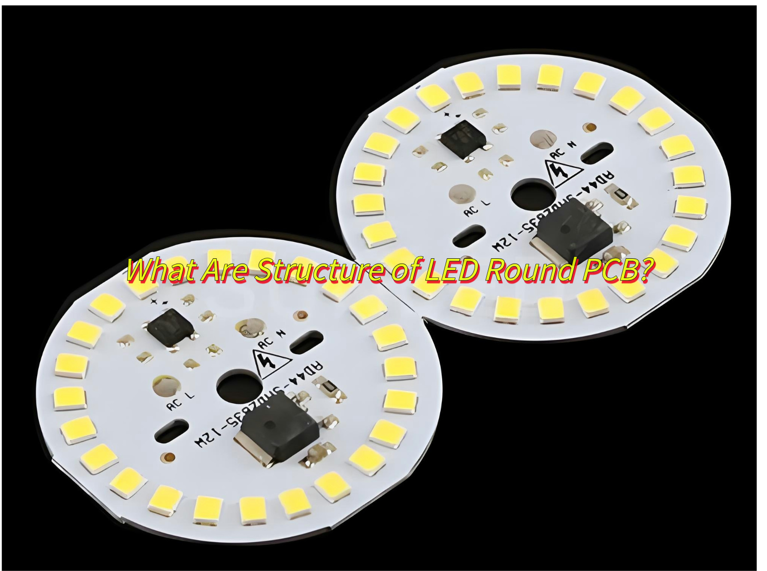
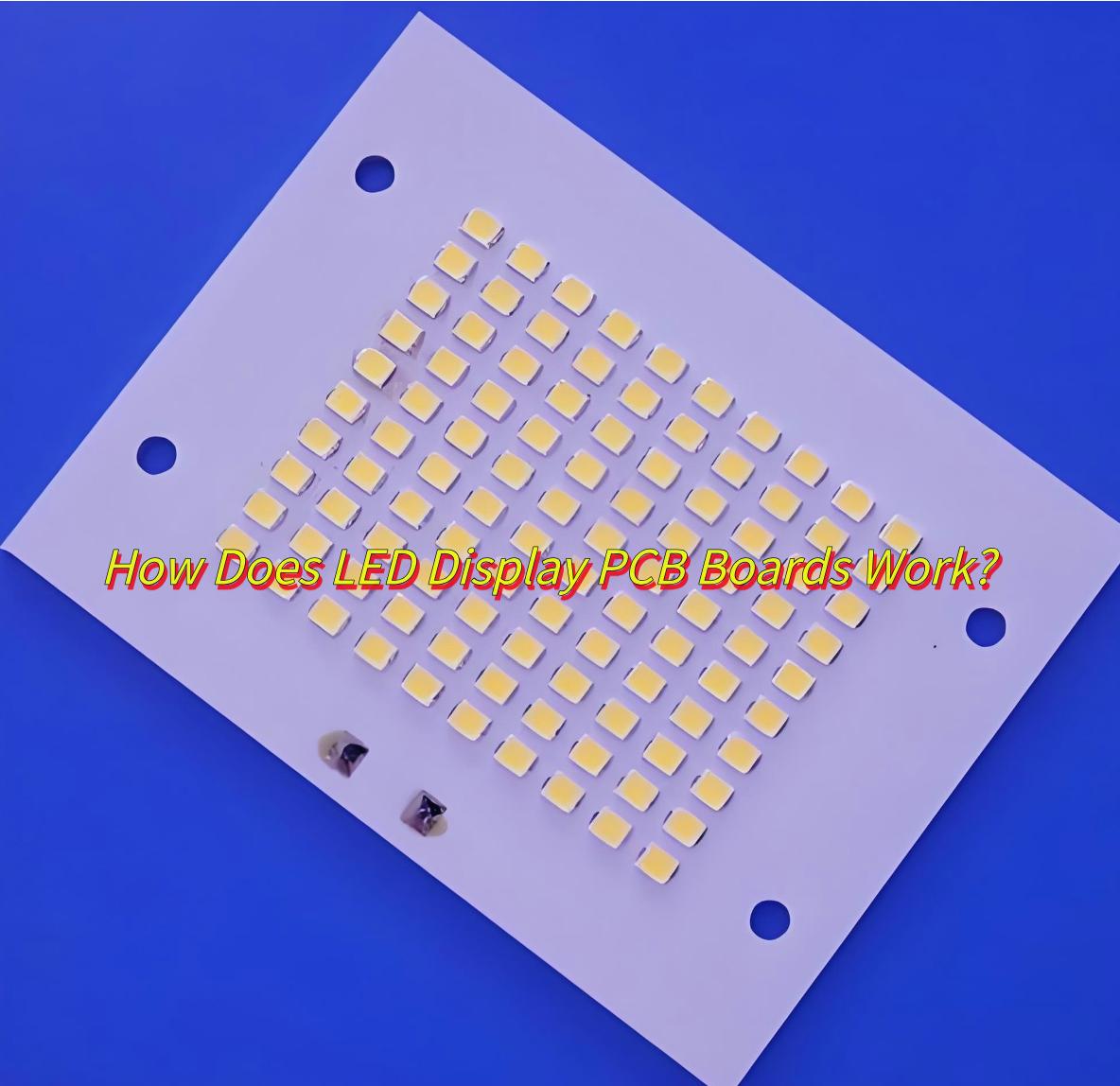
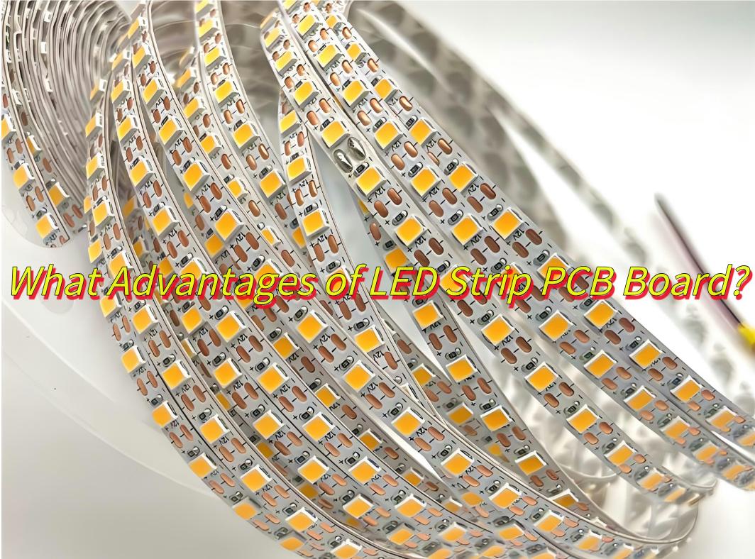
What is LED PCB?
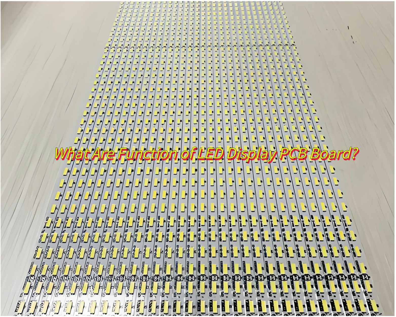
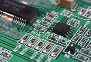
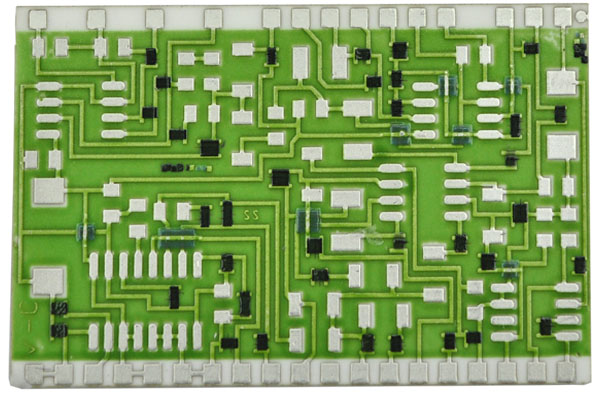
Just as its name implies, LED PCBs are specialized circuit boards designed to power and support LED (Light Emitting Diode) lights. These PCBs must manage heat efficiently and distribute power effectively to handle the electrical load and heat generated by LEDs. They provide the essential platform for mounting LEDs and connecting them to other electronic components. LED PCBs are used in a wide variety of applications, ranging from basic light fixtures to sophisticated lighting systems in automotive, signage, and consumer electronics.
Typically, LED PCBs are made from materials with high thermal conductivity, such as aluminum or copper, to effectively manage heat. The design of these boards varies depending on the type of LED chips, such as surface-mount (SMD) LED or through-hole. LED PCBs also come in various forms, including flexible, rigid, and semi-flexible options, each tailored to specific lighting applications. Regardless of the type, careful attention to the LED PCB design is essential to achieve optimal performance and efficiency.
LED PCB Design Basics
Actually, the basics of a LED PCB design is a deep understanding and practice of both electrical and thermal engineering principles. LED circuit boards differ from standard PCBs because they must support higher currents and dissipate more heat. Therefore, careful planning is required in selecting materials, components, and layout strategies to ensure long-term reliability and efficiency.
At its core, LED PCB design focuses on three main factors:
- Thermal Management: LED devices generate heat, which can damage the components if not managed correctly.
- Current Distribution: The PCB must handle the specific current requirements of each LED.
- Power Design: Since LEDs operate at specific voltages and currents, the power supply must be designed to match these needs.
5 Commonly Used LED PCB Design Software
Before starting a LED PCB design, let’s know the commonly used software during the design process. These tools can help to handle complex circuits, including component placement, routing, and thermal management. It can save much time and money for us.
1. Altium Designer
Altium is a powerful tool known for its user-friendly interface and extensive design features. It offers comprehensive options for both schematic capture and PCB layout, it is a popular choice for professional LED PCB design.
2. Eagle
For smaller business and hobbyists, Eagle is a good choice because it offers an easy-to-use interface and a solid set of features to creating LED circuit boards without steep learning curves.
3. KiCad
KiCad is an open-source and free PCB design tool that is well-regarded for its flexibility and cost-effectiveness. It’s suitable for users who need a more customizable design solution.
4. Mentor Graphics PADS
PADS is well-suited for complex and high-performance PCB designs, particularly for high-frequency LED applications that demand precision and accuracy.
5. DipTrace
DipTrace offers a combination of schematic capture and PCB layout in a user-friendly environment. Its drag-and-drop interface helps reduce design time.
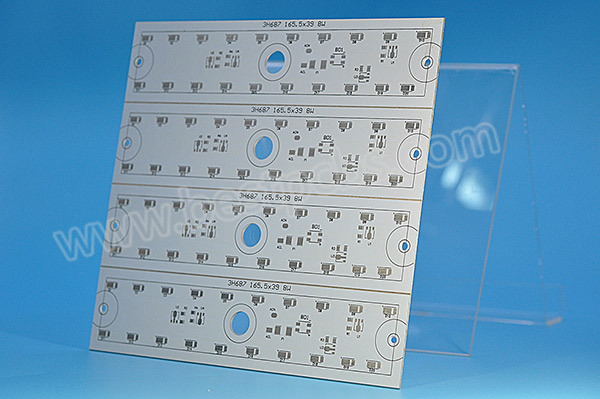
How to Design a LED Circuit Board? – Step by Step
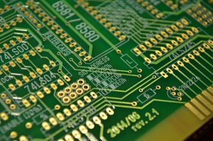
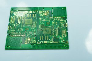
A good LED circuit board is based on a good LED PCB design. When you have a clear ideal and thought about your LED PCB, then you can start designing your PCB. Same as normal FR4 PCB, the LED PCB design starts from schematic drawing – layout – trace wiring – power integrity checking.
1. LED PCB Schematic Diagram Design
This diagram serves as the foundation for the PCB design, so any errors at this stage can lead to problems in the final board. Using a reliable schematic diagram tool to draw your circuit accurately and efficiently. Additionally, avoid overly complex circuits with multiple connections in a single diagram. Keeping the schematic clear and simple will make troubleshooting easier and ensure the design process progresses without issues.

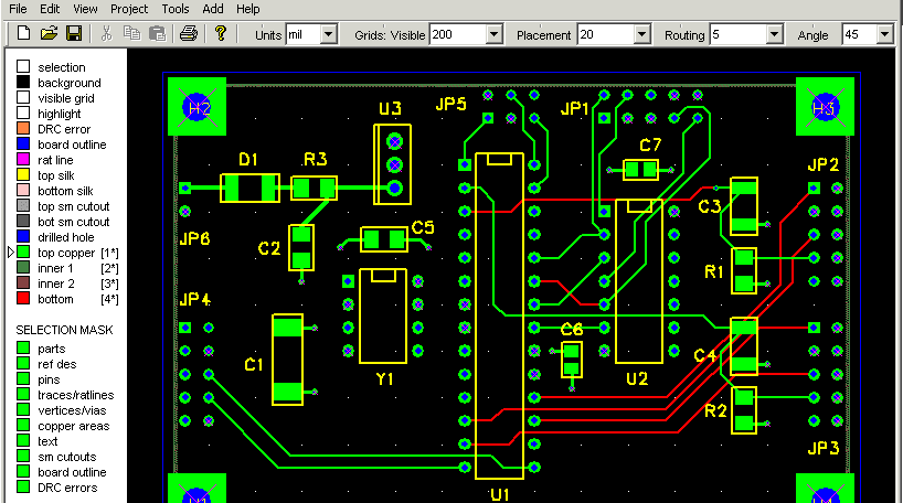
2. LED PCB Layout
Once the schematic is finalized, the next step is the PCB layout. This involves placing the components and routing the traces that will carry the electrical signals to power the LEDs. This stage directly impacts the PCB’s performance, so precise planning and routing are essential. During the pcb layout, remember these tips:
- High-power LEDs should be placed in areas with good airflow or close to heat sinks. It’s also important to keep resistors and power supply components away from heat-sensitive parts.
- To ensure that the traces can handle the required current without overheating, you need to calculate the trace width. Tools like IPC-2221 or use our Online PCB Trace Width Calculators can help determine the appropriate width based on the current and copper thickness used in the PCB. For example, a 1oz copper PCB might need a trace width of 2mm to carry a 2A current safely.
- Using separate power and ground planes to avoid voltage drops and noise. Power planes provide a low-resistance path for high-current traces, while ground planes help with signal integrity and reduce noise.
- Thermal vias are often used to transfer heat from the LED to the PCB’s back layers or heat sinks. For high-power LEDs, these vias must be carefully placed to ensure that heat is efficiently dissipated.
3. LED PCB Wiring
Wiring refers to the creation of the electrical traces that connect the components on the PCB. Compared with FR4 PCB, wiring an LED circuit board is generally straightforward, but attention to detail is essential, particularly when it comes to the lead lengths of each component in the LED PCB design. Typically, the cathode lead is the shortest and connects to the same socket as the anode. Similarly, the resistor should be connected to the anode’s socket, and the other wire, often red or black, should follow the same principle.
Here are some important LED PCB design guidelines for wiring the LED circuit board:
- Component Selection: Before starting the design, choose the LED components based on the specific requirements of your LED circuit board.
- Plan the Wiring Layout: Carefully plan your LED PCB wiring layout and double-check its accuracy before proceeding with the wiring process.
- Via and Trace Optimization: Minimize the use of vias, as they can introduce resistance and inductance. If vias are necessary, ensure they are appropriately sized and placed to handle the current.
- Proper Grounding: Ensure that all LED components in the PCB design are correctly grounded to the circuit board.
- Wire Gauge Selection: Use the appropriate wire gauge for each section of the LED PCB, depending on the current load in each path.
- Prevent Interference: If any wire leads cross over other conductive paths, clamp them securely to prevent interference or accidental contact with other components.
- Heat Shrinking: Apply heat shrink tubing to exposed wire junctions to protect against interference and reduce the risk of short circuits.
- Signal Routing: Ensure that signal traces (such as PWM signals in RGB LED designs) are routed separately from power traces to prevent interference and maintain signal integrity.
- Continuity Check: Before powering up your LED PCB, check for continuity throughout the circuit to ensure everything is connected properly.
- Power Source: Always use an approved power supply when connecting external voltage to the LED PCB.
- Final Check: Before applying power, make sure there are no short circuits, open circuits, reverse polarity issues, or incorrect component placements.
- Test the LEDs: Regularly test the LEDs to ensure optimal performance under various operating conditions.
4. LED PCB Power Design and Analyzing
LED PCBs often require specific power designs to prevent overloading and ensure efficient energy consumption. You must consider the input voltage and how power will be distributed across the board. Proper power analysis ensures that the PCB operates within its designed power specifications.
5. LED PCB Signal Integrity Analysis
Signal integrity is an essential aspect of LED PCB design, particularly for high-speed or high-frequency LED applications. Ensuring that signals are not distorted during transmission will improve the overall performance and efficiency of the LED circuit. This phase involves simulating the behavior of the circuit to ensure it performs optimally under various conditions.
- Simulate circuit behavior: Use specialized tools to simulate how the circuit will behave under different loads and environmental conditions.
- Ensure minimal noise: Check for potential interference or noise in the circuit that could affect LED performance.
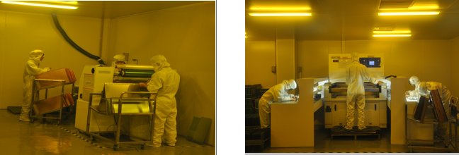
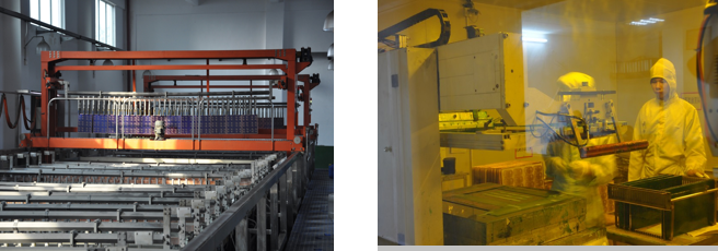
If you are interested in our LED metal core PCB manufacturing process, then the below video will show you all the steps in detailed.
LED Circuit Board Design Considerations
When designing an LED circuit board, several factors must be considered to optimize performance and reliability:
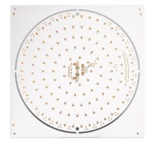
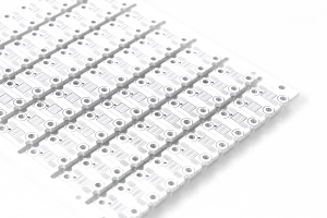
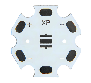
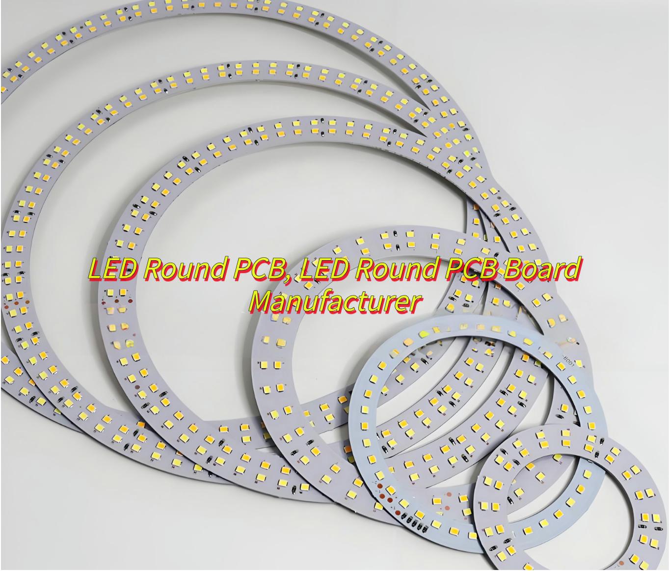
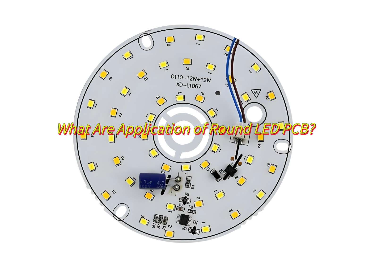
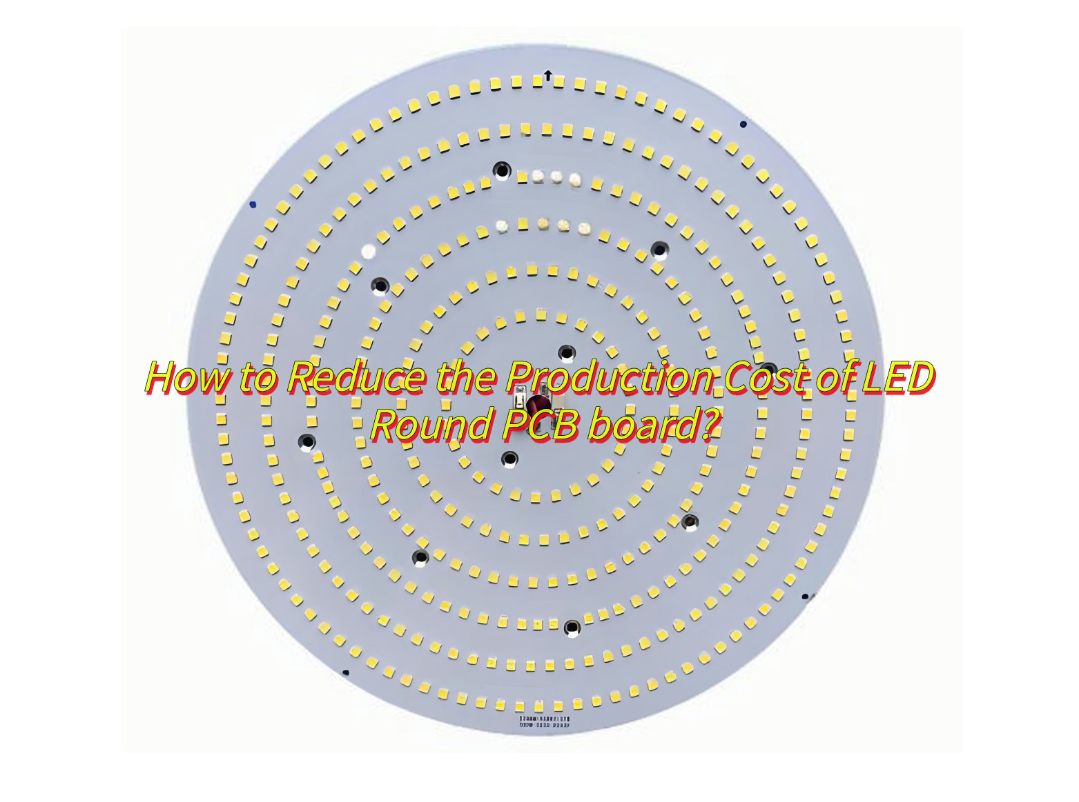
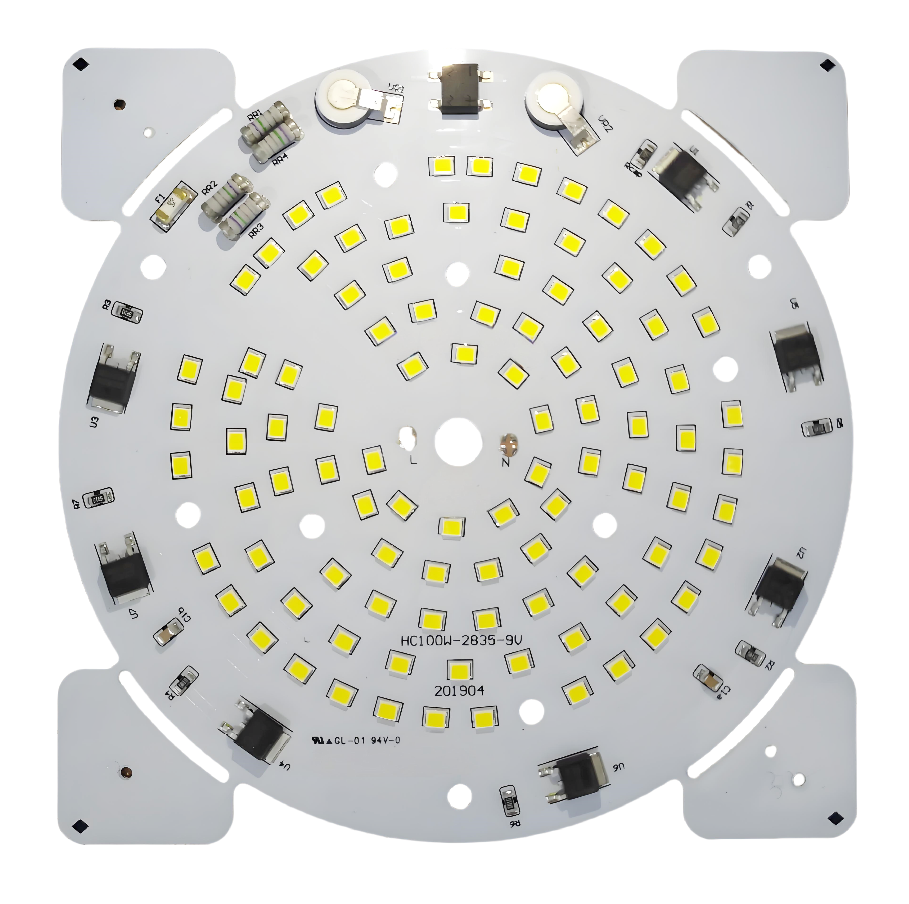
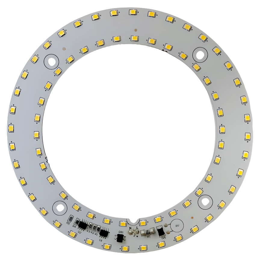
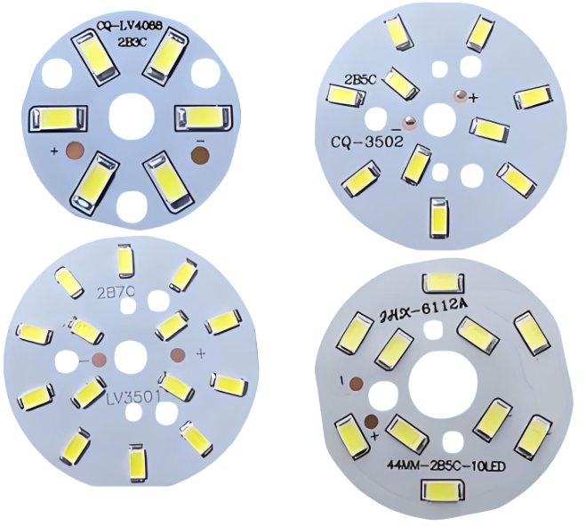
1. Outline Shape
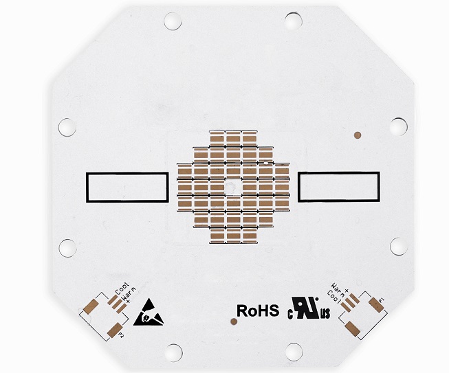
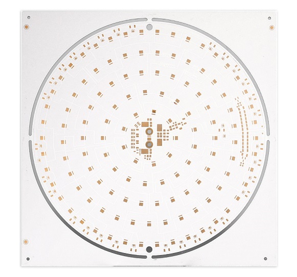
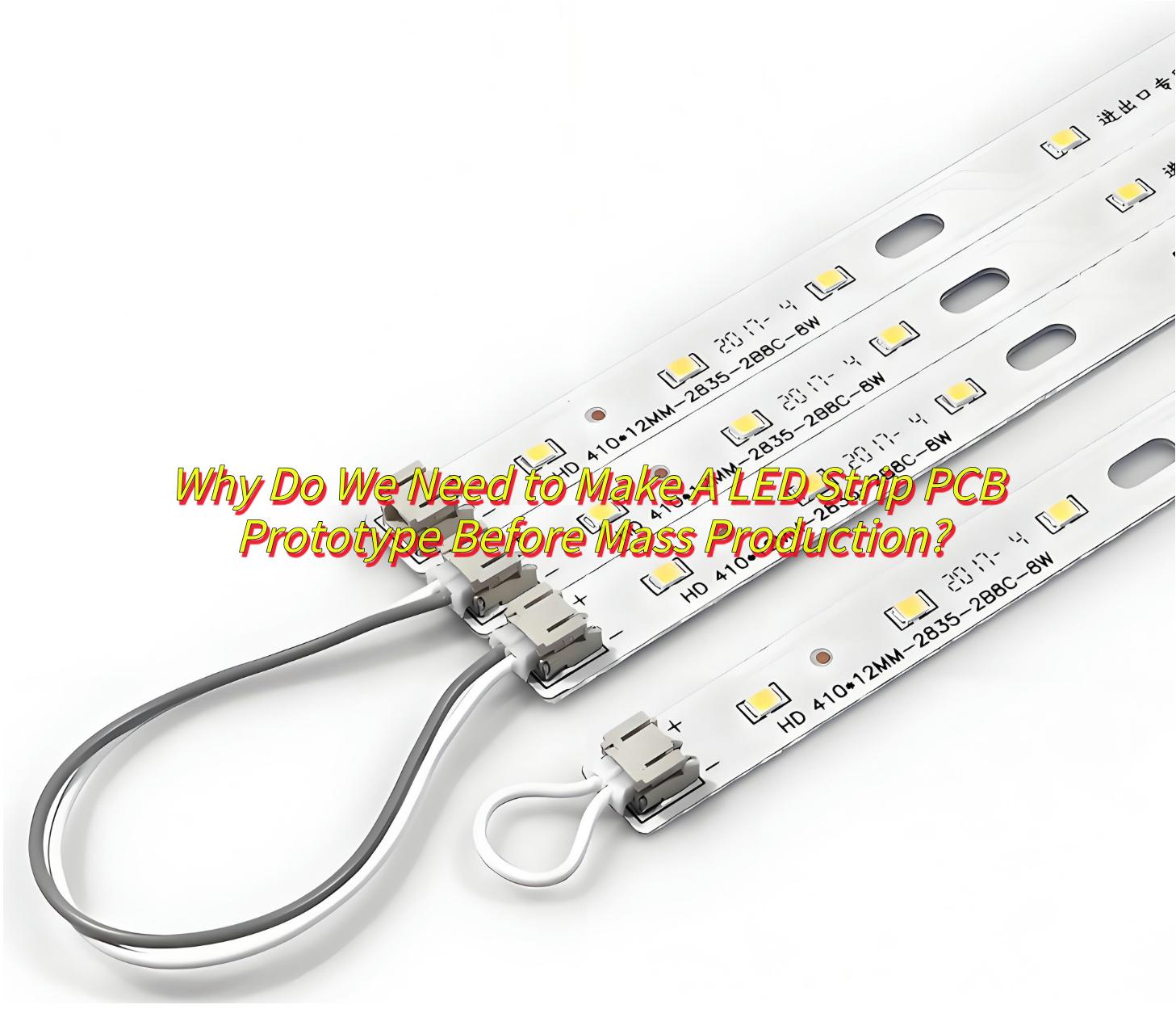
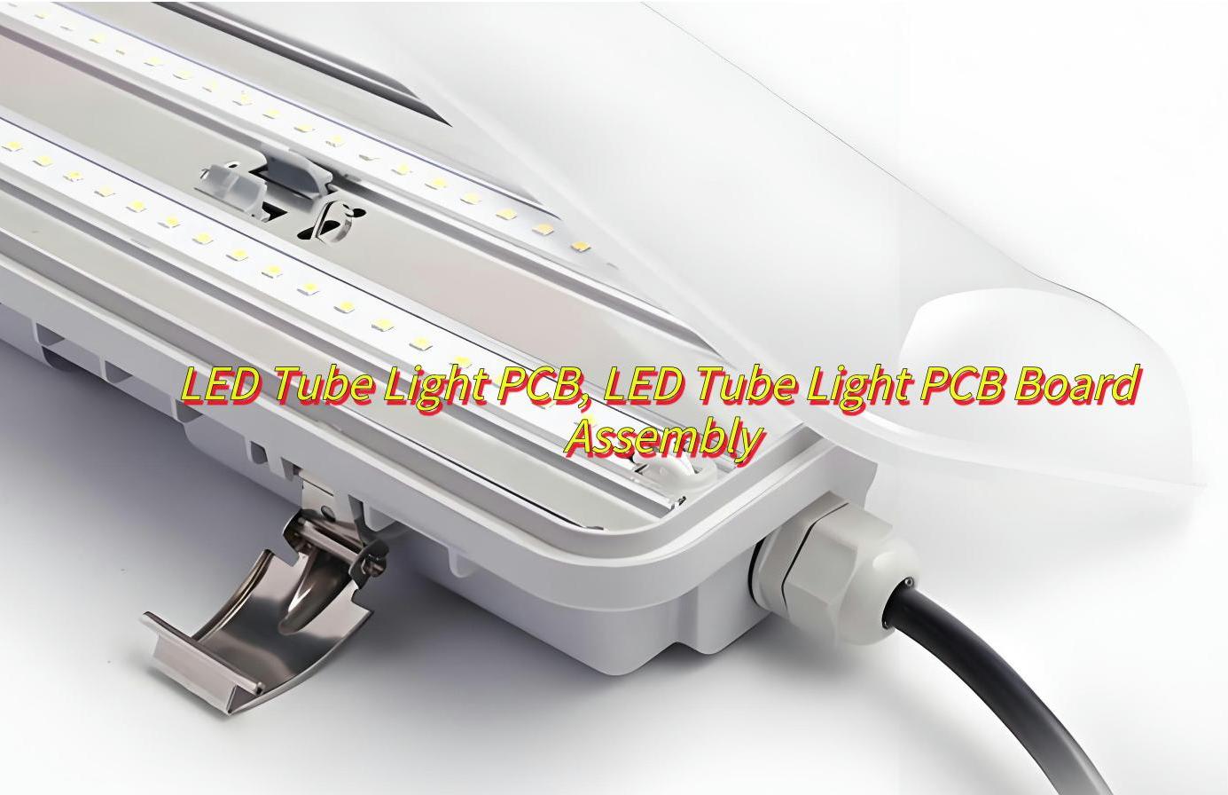
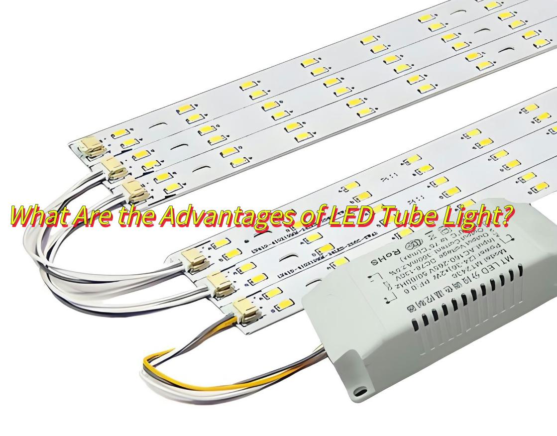
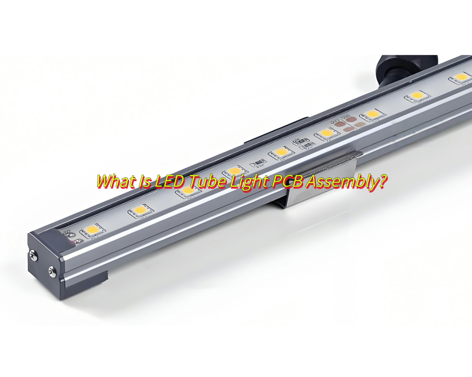
LED PCBs come in various shapes, such as round, rectangular, or custom forms, depending on the final application. For example, LED strip PCBs are often flexible and come in long, narrow shapes, while LED array PCBs may need to accommodate multiple LEDs in a compact rectangular form.
2. Thermal Management
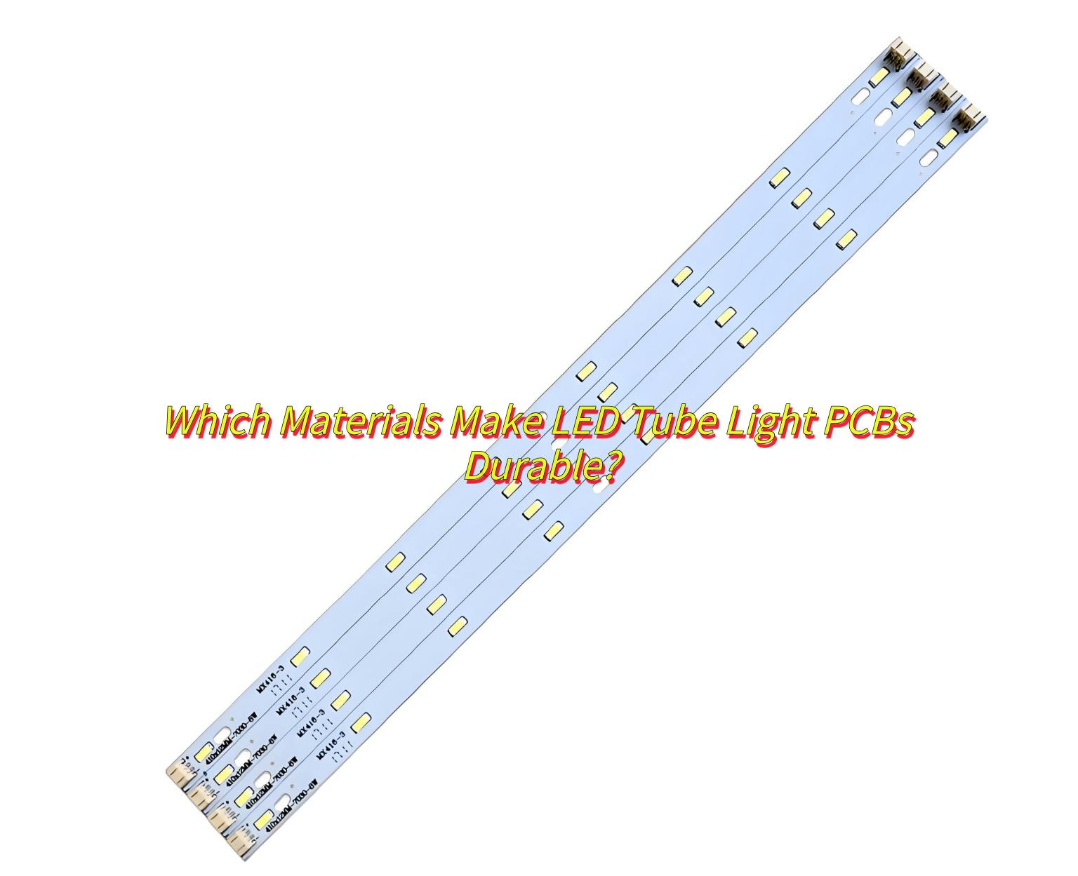
Effective thermal management is one of the most critical considerations when designing an LED PCB. LEDs generate heat during operation, and without proper heat dissipation, performance can degrade quickly, leading to shorter lifespan and possible failure. Aluminum PCBs are often used in LED designs due to their excellent thermal conductivity. Alternatively, copper-clad PCBs may be chosen for high-power applications to ensure that heat is efficiently transferred away from the LEDs.
3. Current Control
Each LED needs a current-limiting resistor to avoid excessive current that could damage the LED. In high-power LED applications, constant current drivers are often used to regulate the current supply.
4. Component Placement
Components should be arranged to minimize heat buildup, reduce interference, and maintain a clean signal path.
- LED Positioning: Place high-power LEDs in areas with better airflow or near heat sinks. Ensuring adequate space around each LED can help manage heat more effectively.
- Resistor and Capacitor Placement: Resistors and capacitors should be placed near the LEDs to minimize the impact of parasitic inductance or resistance. Proper placement also improves the overall efficiency of the circuit and minimizes signal loss.
5. Layout Optimization
The layout takes into account signal integrity and power integrity. In the layout, you need to follow the following principles:
- Power and signal lines should be as wide as possible to reduce resistance and inductance.
- The length of the power and signal lines should be as short as possible to reduce signal delay and noise.
- Sensitive signal lines should be kept away from noise sources, such as motors, switches, etc.
- The arrangement of power and signal lines should take into account the issue of electromagnetic interference (EMI).
LED PCB Design Success Cases at Best Technology
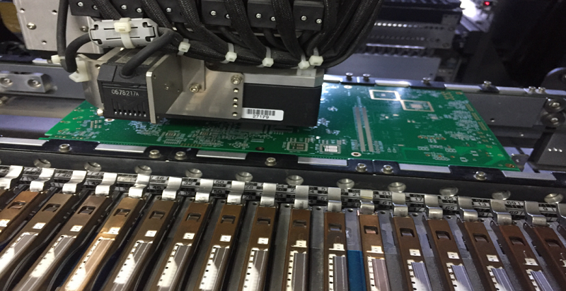
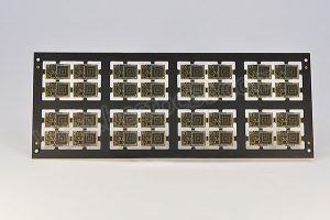
Best Technology is a leading LED PCB manufacturer in Shenzhen China, a city famous of its well-developed electronics industry. Since established in 2006, we have rich experiences in metal core PCB manufacturing, including every aluminum LED PCB and copper core LED PCBs. Different with FR4 PCB, the key manufacturing difficulty of LED PCB is its lamination between dielectric and base, we deeply know its importance, so we set a separate lamination department with experience operators to solve this problem. Additionally, our factory equipped with advanced manufacturing machines to improve our capacity and efficiency. With strong R&D team, we are able to offer better LED PCB design solution to our customers, ensure one-time prototype success. Below, we highlight several success cases that demonstrate how we served our customers.
1. High-Power LED PCB Design for Street Lighting
Customer Challenge:
One of our clients, a leading provider of outdoor lighting solutions, approached us with a high-power LED streetlight project. The primary difficulty they faced was heat dissipation. LED streetlights generate a significant amount of heat, and without effective thermal management, the lifespan of the LEDs would dramatically decrease, leading to frequent failures and increased maintenance costs. The client needed a robust and reliable LED PCB design that could handle the heat produced by high-power LEDs while ensuring energy efficiency and long operational life.
Our Solution:
We suggested aluminum-based PCBs since it has better thermal conductivity than FR4 PCB. To improve heat dissipation further, we added thermal vias and designed the layout to maximize the heat transfer from the LEDs to the surface. In this way, heat sinks can be removed to save some spaces and costs. Additionally, we incorporated constant-current drivers to maintain a stable power supply and prevent current surges that could further exacerbate the heating issue.
Outcome:
Our high-power LED PCB design successfully met the client’s stringent requirements. The energy-efficient design led to reduced operational costs, and the improved thermal management extended the lifespan of the streetlights.
2. RGB LED PCB Design for Swimming Pool
Customer Challenge:
A client in the entertainment industry required a RGB LED PCB for dynamic visual displays in a large-scale concert venue. The biggest challenge was ensuring color accuracy, brightness consistency, and signal integrity across a large array of LEDs. Given the complexity of RGB mixing, the client needed a design that would maintain color uniformity and prevent color distortion or flickering, especially during high-speed color transitions.
Our Solution:
We tackled the signal integrity problem by carefully routing the RGB signal traces to minimize interference and crosstalk. We also integrated pulse-width modulation (PWM) to control brightness, allowing for smooth color transitions and fine-tuned brightness control. The PCB layout included dedicated ground planes to prevent noise from power traces and ensured that the voltage regulators could handle the high current demands without introducing voltage fluctuations that could impact color performance.
Outcome:
The final design ensured vibrant, accurate colors and consistent brightness, even across large areas of the display. The client was able to achieve visually stunning, seamless light transitions for dynamic effects, greatly enhancing the overall viewing experience.
3. SMD LED PCB Design for Compact Devices
Customer Challenge:
A customer in the consumer electronics industry needed an SMD LED PCB for a handheld device. The main challenge here was to design a compact PCB that could handle the power requirements of high-brightness LEDs without compromising the device’s sleek profile. Additionally, the customer faced the issue of heat buildup in such a confined space, which could negatively affect both performance and lifespan.
Our Solution:
To accommodate the client’s space constraints, we employed fine-pitch SMD LEDs and used multi-layer PCB technology to stack components vertically. This allowed us to maximize the use of the available space while maintaining efficient current flow and power distribution. For heat dissipation, we incorporated thermal vias and copper planes to spread heat away from the LEDs. Our design also included current-limiting resistors and voltage regulators to stabilize the power supply to each LED, ensuring consistent performance despite the small size of the PCB.
Outcome:
The customer was extremely satisfied with the reliable, long-lasting solution, which became a cornerstone feature of their product line.
4. Simple LED PCB Design for Residential Lighting
Customer Challenge:
A client in the home lighting industry required a simple LED PCB for mass production of affordable, energy-efficient residential lighting solutions. The challenge was to design a PCB that was both cost-effective and reliable, while ensuring that the LEDs would not overheat or burn out prematurely, especially in long-duration use cases.
Our Solution:
For this project, we designed a single-layer PCB to minimize costs while maintaining functionality. We incorporated current-limiting resistors to protect the LEDs and used low-cost components that could be easily sourced for mass production. Thermal considerations were addressed by optimizing the component placement and providing ample space around the LEDs for heat dissipation. We also ensured the design could handle voltage fluctuations by incorporating a voltage regulator.
Outcome:
The design resulted in a highly affordable, yet durable LED PCB that was well-suited for high-volume production.
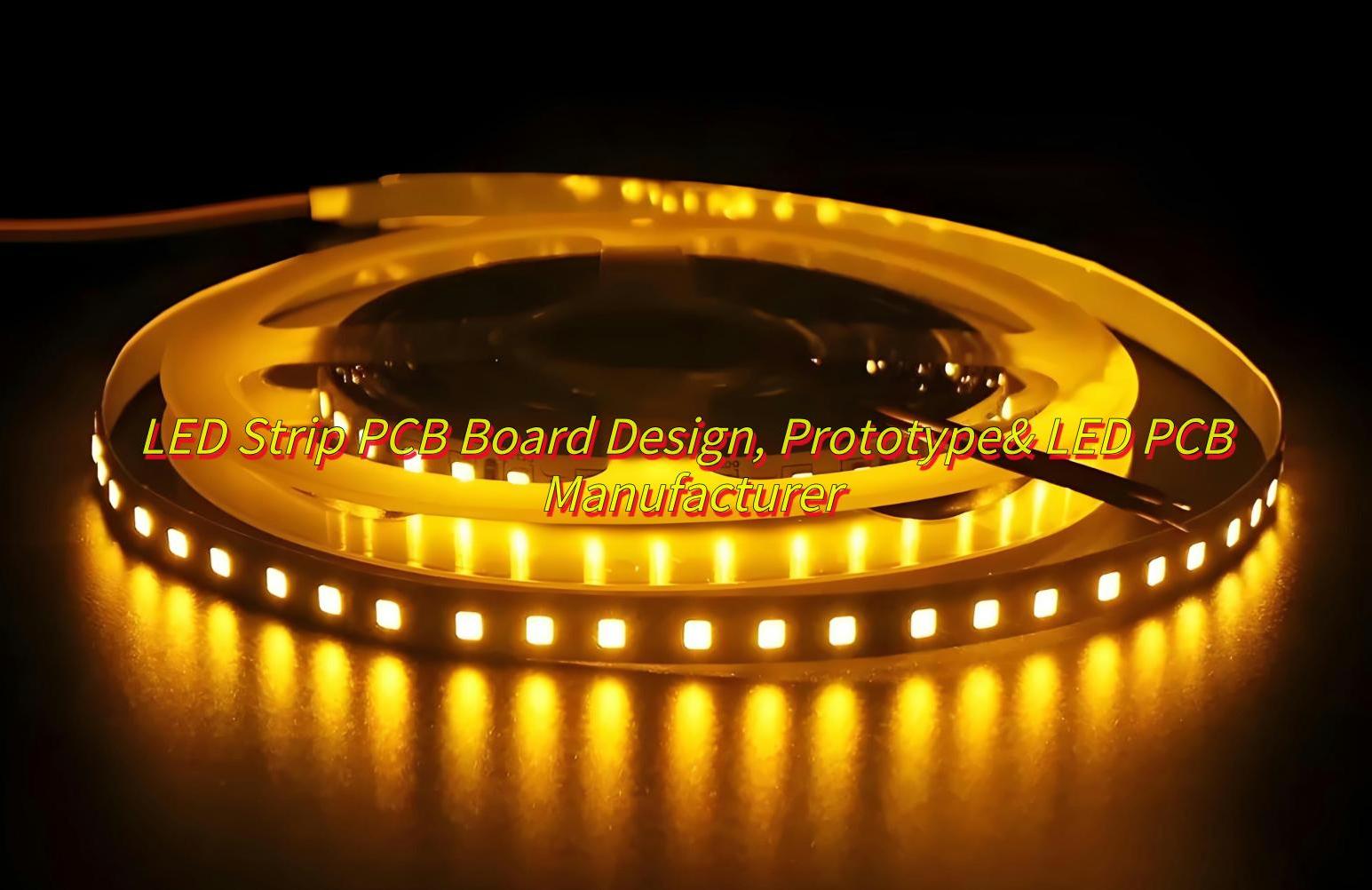
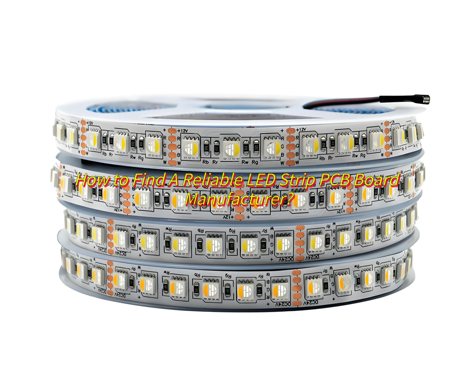
5. Flexible LED Strip PCB Design for Custom Installations
Customer Challenge:
A client involved in decorative lighting for both residential and commercial spaces required a flexible LED strip PCB that could be easily bent and shaped around various installations. The major hurdle was ensuring consistent power distribution along the strip while maintaining a compact and flexible design. The client also needed the strips to withstand outdoor conditions without compromising on performance.
Our Solution:
We designed the flexible LED PCB using polyimide film for its excellent flexibility and durability. To ensure uniform brightness across the entire length of the strip, we used constant voltage circuits and low-resistance traces to minimize power loss. We also applied encapsulation to protect the PCB from environmental factors such as moisture, UV rays, and physical wear and tear.
Outcome:
The resulting LED strip was not only flexible but also highly durable and weather-resistant, making it suitable for both indoor and outdoor use. The customer was able to offer a customizable, high-quality lighting solution that could be used in a wide range of applications, from commercial signage to home decor.
FAQs
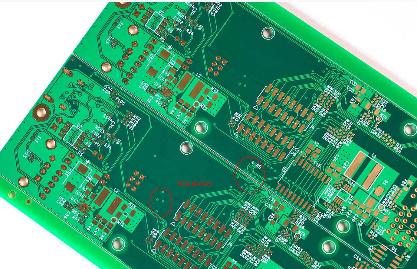
Q1: Are the via’s important for the thermal conduction?
From the via’s perspective, the via can be helpful in thermal conduction. At the same time, it is not that more heat dissipation through holes is better. The design of Via needs to be followed the minimax distance between holes. From the metal core material, the copper material is better than aluminum core in same situation. And sinkpad copper core PCB is better than copper core PCB. Because the convexity pad will be helpful in thermal conductivity. From the dielectric film, the 3W material is best. 2W material is better than 1W material. From the design of metal core PCB, the larger the area of solder mask opening means the larger the exposed copper surface outside, and the better the heat dissipation effect.
Q2: Does the dielectric in MCPCB cause problems at high temperatures?
The dielectric in MCPCB will cause problems at high temperatures, and the dielectric layer of MCPCB is the bottleneck of high temperature, because the Tg value of the layer is only 130℃.
Q3: What is the thickness of the thermal conductivity?
0.8W/m.k,Thickness=50-75um
1.0W/m.k,Thickness=75-100um;
1.5W/m.k,Thickness=100um
2.0W/m.k,Thickness=100-125um;
3.0W/m.k,Thickness=125-200um
For the breakdown, it is bigger when the line space is wider and the dielectric layer is thicker. Normally, the copper thickness is 10Z and 2OZ and surface finishing is HASL(LF), ENIG and OSP.
Q4: Can the aluminum be made as the base of sinkpad MCPCB?
Actually, the sinkpad can only use copper as the base. Because the SinkPad will etch the copper base into convex platform with Copper Etching Solution, then hollow out the Double Layer FR4 PCB, and do lamination with the convex platform. However, regarding of current technical conditions, since aluminum or aluminum alloy cannot directly react with acid, the reaction process is too complex and difficult to control, which will increase the difficulty of etching the LED pad platform. Considering the scrap rate, the process of etching LED pad platform with aluminum is more complex and the overall cost is higher.
Q5: It is possible dielectric + top metal layer to be >500um for wire bonding?
The dielectric layer and metal layer don’t affect the wire bonding, it depend on ENEPIG thickness, we do a lot of this kind of boards for our customers, as long as the do it with 3u”, then it is very good for wire bonding. If you insist on needing dielectric + top metal layer to be >500um, then the copper thickness need to be 10 OZ(350um), the price will be very high.