pcb
Home > Blog

Archive for the ‘Ceramic PCB’ Category

Everything you should know about Tg in PCB
Wednesday, January 4th, 2023

Working temperature changes can have a significant influence on the operation, reliability, lifetime and quality of products. Temperature rises results in materials expanding, however,Ā the substrate materials that PCB are made ofĀ have different thermal expansion coefficients, this causesĀ mechanical stress that can create micro-cracksĀ that may be undetected during electrical tests carried out at the end of production.

Due to the policy of RoHS issued in 2002 requiredĀ lead-free alloys for soldering. However, removing lead directly results in the rise of melting temperature,Ā printed circuit boards are therefore subject to higher temperaturesĀ during soldering (including reflow and wave). Depending on the chosen reflow process (single, doubleā€¦), it is necessary toĀ use a PCB with appropriate mechanical characteristics, especially one with suitableĀ Tg.Ā 

What is Tg?

Tg (glass transition temperature) is the temperature value that guarantees the mechanical stability of the PCB during operational life time of the PCB, it refers to the critical temperature at which the substrate melts from solid to rubberized liquid, we called the Tg point, or melting point for easy to understanding. The higher the Tg point is, the higher the temperature requirement of the board will be when laminated, and high Tg board after laminated will also be hard and brittle, which benefits for next process such as mechanical drilling (if any) and keep better electrical properties during use.
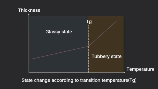
The glass transition temperature is hard to be measured accurately in considerate many of factors, as well as each material have its own molecular structure, therefore, different materials have a different glass transition temperature, and two different materials may have the same Tg value even they have different characteristics, this enable us to have an alternative choice when the needed material is out of stock.

Features of High Tg materials

  • Better thermal stability
  • Good resistance to moisture
  • Lower thermal expansion coefficient
  • Good chemical resistance than low Tg material
  • High value of thermal stress resistance
  • Excellent reliability

Advantages of High Tg PCB

In general, a normal PCB FR4-Tg is 130-140 degrees, the medium Tg is greater than 150-160 degrees, and high Tg is greater than 170 degrees, High FR4-Tg will have better mechanical and chemical resistance to heat and moisture than standard FR4, here are some advantages of high Tg PCB for your reviewing:

  1. Higher stability: It will automatically improve the heat resistance, chemical resistance, moisture resistance, as well as stability of the device if increasing the Tg of a PCB substrate.
  2. Withstand high power density design: If the device has a high power density and a fairly high calorific value, then high Tg PCB will be a good solution for heat management. 
  3. Larger printed circuit boards can be used to change the design and power requirements of the equipment while reducing the heat generation of ordinary boards, and high Tg PCBS can also be used. 
  4. Ideal choice of multi-layer and HDI PCB: Because multi-layer and HDI PCB are more compact and circuit dense, it will result in a high level of heat dissipation.Ā  Therefore, high TG PCBs are commonly used in multi-layer and HDI PCBs to ensure the reliability of PCB manufacturing.
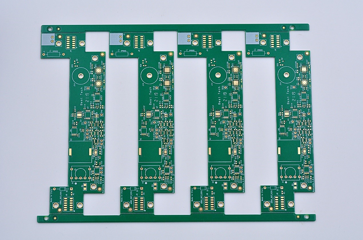
When do you need a High Tg PCB?

Normally to ensure the best performance of a PCB, the maximum operating temperature of the circuit board should be about 20 degrees less than the glass transition temperature. For example, if the Tg value of material is 150 degrees, then the actual operating temperature of this circuit board shouldnā€™t more than 130 degrees. So, when do you need a high Tg PCB?

  1. If your end application requires to bear a thermal load greater than 25 degrees centigrade below the Tg, then a high Tg PCB is the best choice for your needs.
  2. To make sure the safety when your products require an operating temperature equal or greater than 130 degrees, a high Tg PCB is great for your application.
  3. If your application requires a multi-layer PCB to meet your needs, then a high Tg material is good for the PCB.

Applications that require a high Tg PCB

  • Gateway
  • Inverter
  • Antenna
  • Wifi Booster
  • Embedded Systems Development
  • Embedded Computer Systems
  • Ac Power Supplies
  • RF device
  • LED industry

Best Tech has rich experience in manufacturing High Tg PCB, we can make PCBs from Tg170 to maximum Tg260, meanwhile, if your application need to use under extremely high temperature like 800C, you’d better use Ceramic board which can go through -55~880C.

You may also like

Suitable Choice of Ceramic Substrate for Your Application
Wednesday, December 7th, 2022

With the rapid development of ceramic industry, Ceramic Circuit Board is widely used in semi-conductors and electronic packages fields because it provides an excellent electric conductivity, low thermal expansion and good insulation properties over standard FR4 based PCBs. As you can see from our website: https://www.bestpcbs.com/products/ceramic-substrate.htm, there are various kinds of ceramic substrate materials in the market, different materials have different functions and properties. Here we illustrated the different kinds of materials in the market as below for you to choose which one is ideal for your designs when needs come out.
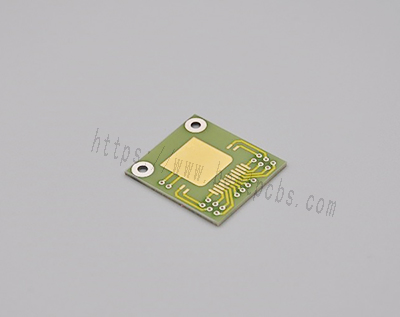
Common ceramic substrate materials

Nowadays, the most commonly material in the market is oxidation material, it always used in automobile products as its wear resistance and good strength.

Besides, there are some nitrides and silicious can be used in high power products.

For a quick look, here I listed as following:

  • Alumina Oxide (Al2O3)
  • Alumina Nitride (ALN)
  • Beryllium Oxide (BeO)
  • Silicon Nitride (Si3N4)
  • Zirconium Oxide (ZrO2)
  • Silicon Carbide (SiC)

Characteristics of different substrate materials

Alumina Oxide (Al2O3)

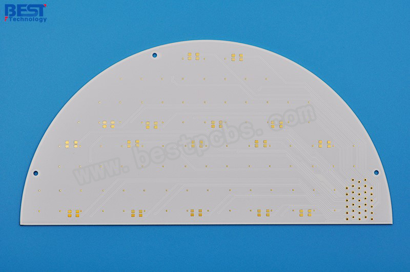
Alumina substrate characterize as a pure white substrate and the most commonly used ceramic substrate material in the electronics industry because of its high strength and chemical stability compared to most other oxide ceramics in terms of mechanical, thermal and electrical properties, and the richful source of raw materials is suitable for a variety of technical manufacturing and different shapes. The most commonly used Alumina Oxide are 96% alumina and 99.6% alumina.

  • 96% alumina can be used to fabricate Thick Film Ceramic Circuits as it has excellent electrical insulation, mechanical strength, good thermal conductivity, chemical durability and dimensional stability. The surface roughness is generally 0.2~0.6Ī¼m, and the maximum using temperature of the substrate can reach 1600ā„ƒ
  • 99.6% alumina is the mainstay of most Thin-film electronic substrate applications, commonly used in circuit generation for sputtering, evaporation and chemical vapor deposition of metals. 99.6% alumina has higher purity, smaller grain size, and excellent surface smoothness than 96% alumina (the surface roughness is generally 0.08~0.1Ī¼m), and it can withstand maximum 1700Ā°C temperature when applied in applications.

Alumina Nitride (ALN)

Currently, Alumina Nitride won the high attention of the public by means of two key excellent properties: one is high thermal conductivity. Alumina nitride offers a big increasing in thermal conductivity (170Wm.k), which is approximately 100-200 times than FR4 substrates did, while alumina oxide only offers 24W/m.K.

Another characteristic is silicon-matched expansion coefficient of 4.7ppm/Ā°C 20~300Ā°C, this makes it suitable for used in extremely harsh environments likely in high temperatures. The disadvantage is that even an extra thin oxidation will affect the thermal conductivity. Only by strictly controlling the material and process, can aluminum nitride substrate be produced with good consistency. Thatā€™s why the alumina nitride is expansive than alumina oxide.

By visually, alumina nitride has an off-white color, that give us a chance to distinguish it with alumina oxide easily.

Beryllium Oxide (BeO)

Beryllium Oxide has a high thermal conductivity than alumina, therefore, it almost used where high thermal conductivity required.  But when the temperature exceeds 300Ā°C, it drops quickly. It is not as widely used as alumina oxide or aluminum nitride, the most important thing is that its toxicity limits its development.

Silicon Nitride (Si3N4)

Silicon Nitride is a material with high fracture toughness and strong heat resistance are often used as alternative materials for modules in recent years. With strong mechanical, high temperature resistance, corrosion resistance and wear resistance, it is widely used in automotive shock absorber, engine, especially automotive IGBT products, as well as traffic track, aerospace and other fields.

Zirconium Oxide (ZrO2)

Zirconium Oxide is popular as its exceptional strength, toughness, biocompatibility, high fatigue and wear resistance (15times of alumina oxide) render it optimal for dental applications.

Silicon Carbide (SiC)

The essence of silicon carbide ceramic substrate is a silicon material, which determines its high current density characteristics due to its superior thermal conductivity.

In the meantime, the higher band gap width determines the higher breakdown field and higher operating temperature of silicon carbide (SiC) ceramic circuit board. 

The core advantages of silicon carbide are high temperature resistance, high pressure resistance, wear resistance, low loss and high frequency work.Ā  Therefore, it is used for products with high heat dissipation, high thermal conductivity, large current, large voltage and high frequency operation.

Send us inquiry for fabrication

At present, you should have a brief acknowledge about different ceramic substrate materials and their characteristics, and you should be able to decide which materials is most suitable for you. If you still have some concerns or different opinions about substrate for Ceramic pcb, welcome to contact us, Best Tech will offer you free advice and technical support for ceramic substrate choice.

You may also like

Why ENEPIG More Suitable for Ceramic PCB Wire Bonding?
Thursday, October 20th, 2022

There are many surface treatment choices that can be used on Ceramic PCB, but why ENEPIG is one of options we always recommend to our customers whom have wire bonding demands?

In the application of Ceramic PCB, COB or wire bonding was widely used for the packaging technology in thin, short, high speed of electronic products. The Chip On Board (COB) technology refers to a technology in which bare chips are directly attached to the PCB board and then connected electronically through metal wires, namely ā€œWire Bondingā€. Due to gold wire has an excellent electrical conductivity, thermal conductivity, corrosion and oxidation resistance, gold wire is often used as a main bonding material in microelectronics packaging.

What is ENEPIG?

ENEPIG, is a type of surface treatment on Printed Circuit Boards and ceramic PCB, the full name of it is Electroless Nickel ā€“ Electroless Palladium ā€“ Immersion Gold, now it is widely used in wire bonding field.

How does it work and what’s the standard thickness of each layer?

  • Electroless Nickel: Nickel acts as a barrier layer, preventing copper from interacting with the other metals involved in this plating technology, particularly gold. The layer is deposited on the catalytic copper surface using an oxidation-reduction reaction. The result is a layer that is between 2.0 to 5.0 microns thick.
  • Electroless Palladium: Palladium is a relatively stable metal at room temperature, and it is difficult to be oxidized within 400ā„ƒ. The chemically deposited palladium layer has a neat lattice arrangement, uniform grain size and compact structure. Adding palladium layer between nickel layer and gold layer can effectively prevent the diffusion of nickel layer to gold layer. The Palladium is a layer with a thickness between 0.03 to 0.10 microns, it also depends on the final applications.
  • Immersion Gold: The main function of the gold layer is to bond with the gold wire. If there is no palladium layer as a diffusion barrier between the nickel layer and the gold layer, the gold layer can also bond with the gold wire after reflow, as long as the gold layer reaches a certain thickness. For example, when the thickness of the electroplated nickel gold reaches 0.3um, it can bond with the gold wire. In addition, gold itself has a good bonding ability with gold wire, and in ENEPIG process, due to the palladium layer protects the gold layer from the pollution of nickel, only a thin gold layer (0.03um~0.05umm) is needed to have a good bonding property. Thisā€™s why thereā€™s cost advantage of ENEPIG than that of thicker ENIG.
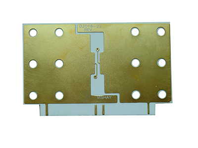
(ENEPIG product)

Why choose ENEPIG?

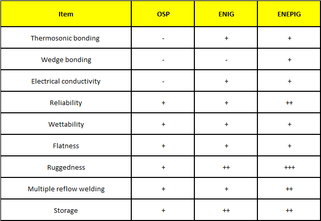
ENIPIG has a good wiring bonding ability, solder joint reliability, multiple reflow soldering and excellent storage time, can correspond to and meet the requirements of a variety of different assemblies.Ā  Below is a comparison about performance of different surface treatments:

(Comparison-about-performance-of-different-surface-treatments)

AdvantagesĀ  of ENEPIG

  • ā€œBlack Nickelā€ free — The palladium layer separates the Nickel layer from the gold layer, it can prevents the mutual migration of gold and nickel, so no black nickel will appear
  • Excellent gold wire bondability — the gold plating/coating is very thin, can be used for gold wire bonding as well aluminum wire bonding
  • Palladium acts as an additional barrier layer to further reduce copper diffusion to surface, thus ensuring good solderability
  • Cost-effective than ENIG
  • Lead-free nickel
  • Good compatibility between coating and solder paste
  • Very suitable for packaging components such as SSOP, TSOP, QFP, TQFP, PBGA

Best Technology is a 16+ years PCB manufacturer and we made many ENEPIG PCBs and ceramic PCBs for our customers, welcome to contact us if you have demands on ENEPIG PCB.

You may also like

What are the Factors Affecting the Thermal Conductivity of AlN Ceramic Substrate?
Tuesday, May 31st, 2022

The Introduction of AlN Ceramic

With hexagonal wurtzite structure and no other homomorphic isomers, AlN, aluminum nitride, is a structurally stable covalent bond compound, whose crystal structure is AlN4 tetrahedron formed by the dismutation of aluminum atom and adjacent nitrogen atom. And its space group is P63mc, belonging to hexagonal system.

The Features of AlN Ceramic

  1. High thermal conductivity, which is 5 to 10 times than that of aluminum oxide ceramic.
  2. Coefficient of thermal expansion (4.3*10-6/ā„ƒ) matches the semiconductor silicon material (3.5-4.0*10-6/ā„ƒ).
  3. Great mechanical properties.
  4. Excellent electrical performance, with high insulation resistance and low dielectric loss.
  5. Multi-layer wiring can be carried out to achieve high density and miniaturization of packaging.
  6. Non-toxic, conducive to environmental protection.
Ceramic PCB

Factors Impacting on the Thermal Conductivity of AlN Ceramic

At 300K, the theoretical thermal conductivity of AlN single crystal material is as high as 319 W/(mĀ·K). But in the actual production process, its thermal conductivity will still be affected, which is often lower than the theoretical value due to the influence of various factors such as the purity and internal defects (dislocations, pores, impurities, lattice distortion) of material, grain orientation and sintering process.

Effect of Microstructure on Thermal Conductivity

The heat conduction mechanism of single crystal AlN is phonon heat transfer, hence the thermal conductivity of AlN may be mainly influenced by the scattering control of grain boundary, interface, second phase, defect, electron and phonon itself. In accordance with the solid lattice vibration theory, the relation between phonon scattering and thermal conductivity ā€œĪ»ā€ is as follows: Ī»= L / 3CV.

In the formula, C is the heat capacity; V represents the average velocity of phonons; and L stands for the mean free path. And it can be seen from the equation that the thermal conductivity (Ī») of AlN has direct ratio with the mean free path (L), for which the larger ā€œLā€ is, the higher the thermal conductivity is. From the perspective of microstructure, the scattering can be caused by the interaction between phonons and phonons, phonons and impurities, and phonons and grain boundary.  It will affect the mean free path of phonons, and thus impact on the thermal conductivity.

It can be learnt from above that the microstructure of AlN has a great influence on its thermal conductivity. Therefore, it is necessary to make AlN crystals with fewer defects and impurities in order to obtain AlN ceramics with high thermal conductivity.

Effect of Oxygen Impurities Content on Thermal Conductivity

There are studies show that AlN has a strong affinity with oxygen so that it is easy to be oxidized, leading to the formation of aluminum oxide film on its surface. Owing to the dissolution of oxygen atoms in Al2O3, the nitrogen in AlN is replaced, resulting in aluminum void and oxygen defect. In this way, it will bring about the increase phonon scattering and decrease of mean free path hence the thermal conductivity will be reduced.

Oxygen Content in AlN (wt%)Thermal Conductivity (W/mĀ·K)
0.31130
0.24146
0.19165
0.13171
0.12185

So, it can be concluded that the types of defects in AlN lattice are related to the concentration of oxygen atoms.

  • When the oxygen concentration is lower than 0.75%, oxygen atoms evenly distributed in the AlN lattice, replacing the position of nitrogen atoms. And then the aluminum void is accompanied by it.
  • When the oxygen concentration is not less than 0.75%, the position of Al in aluminum nitride lattice will have a change. Then the aluminum void will disappear, causing octahedral defects.
  • When the oxygen concentration is higher, the lattice will produce extension defects such as polytype, inversion domain and oxygen-containing stacking fault. Moreover, based on thermodynamics, it is found that the amount of oxygen in AlN lattice is under the influence of Gibbs free energy (Ī”GĀ°). The larger the Ī”GĀ° is, the less oxygen is in the lattice, hence there will be a higher thermal conductivity.

Therefore, the thermal conductivity of aluminum nitride is seriously affected by the existence of oxygen impurities, which is a key point resulting in the decrease of thermal conductivity.

Thermal Conductivity can be Enhanced by Suitable Sintering Aids

In order to improve the thermal conductivity of AlN, the required sintering aids need to be added to lower sintering temperature and remove oxygen in lattice.

As matters stand, the addition of multiple composite sintering additives is followed with more interests. And the experiment shows that relatively dense AlN samples with less oxygen impurities and the secondary phase can be obtained by adding the composite sintering aids, Y2O3-Li2O, Y2O3-CaC2, Y2O3-CaF2, Y2O3-Dy2O3, to aluminum nitride.

In a word, selecting appropriate composite sintering additives can help to get lower sintering temperature and effectively purify the grain boundary, so as to obtain AlN with high thermal conductivity.

In case if you have any other questions aboutĀ ceramic PCBĀ orĀ MCPCB, you are welcome to contact us via email atĀ sales@bestpcbs.com. We are fully equipped to handle yourĀ PCBĀ orĀ MCPCBĀ manufacturing requirements.

You may also like

Pros and Cons of the Ceramic PCB
Friday, May 27th, 2022

Ceramic PCB is used in various fields because of its high-quality thermal and mechanical advantages. The boardā€™s unique features and high thermal conductivity have enabled it to be used in devices big and small. But meanwhile, it is not flawless. There are also some disadvantages.

Ceramic PCB

Pros of ceramic PCB

It is supposed that you are familiar with the features below that the ceramic PCB has.

  • Excellent thermal conductivity.
  • Good insulation.
  • High temperature resistance.
  • Great mechanical properties.
  • Compatible with CTE (Coefficient of Thermal Expansion) of components.
  • High-density assembly possible.
  • Non-toxic, conducive to environmental protection.

Cons of ceramic PCB

There are also a few disadvantages that can be found in ceramic PCB. Some of the disadvantages are stated below.

  • Cost—It has a higher cost compared to other printed circuit boards.
  • Handling—Since ceramic is fragile, it entails careful handling. As ceramic PCB is made for tight spaces, it is very small and this makes it even harder to handle.
  • Availability—It is not as widely available.

Everything has two sides. And ceramic PCB has no exception. But if considering all the advantages and disadvantages, ceramic PCB still takes the win amongst all other boards.

So, this is the end of the article about the advantages and disadvantages of the ceramic PCB. In case if you have any other questions about ceramic PCB or MCPCB, you are welcome to contact us via email atĀ sales@bestpcbs.com. We are fully equipped to handle yourĀ PCBĀ orĀ MCPCBĀ manufacturing requirements.

You may also like

Thermal Conductivity—Aluminum PCB vs Ceramic PCB Series 2
Tuesday, April 19th, 2022

Last time we have talked about the structure difference between the aluminum PCB and ceramic PCB. So, based on the different structures, whose thermal conductivity is better?

We have known that a single layer aluminum PCB is made up of copper layer, dielectric layer and aluminum layer. Meanwhile, the dielectric layer is the decisive factor affecting the thermal conductivity.

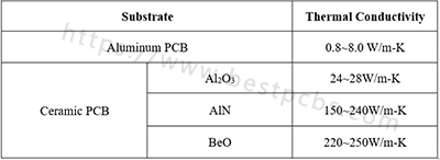
Generally, its thermal conductivity ranges from 0.8 to 3.0 W/m-K, but can up to 8.0 W/m-K. So, in terms of heat dissipation, the aluminum substrate does much better than FR-4 substrate. And it is a good choice for LED lighting products with high power.

Aluminum PCB

However, the heat-conducting property of ceramic PCB is superior to that of the aluminum PCB.

Since ceramic itself is an insulating material with a great heat-conducting property, it does not need a dielectric layer. Therefore, the heat can be dissipated directly through the ceramic.

Because of its excellent performance in heat dissipation, it is particularly suitable for the lighting product with ultra high power and those products which have a high demand of heat dissipation.

Ceramic PCB

To summarize, clearly, we can know from the table below that ceramic PCB does better than aluminum PCB in terms of thermal conductivity and heat dissipation. And this is mainly because of the dielectric layer, which is related to the functions of bonding, insulation and heat conduction.

The better the heat conduction performance of the insulating layer, the more conducive it is to the diffusion of heat generated during the operation to the device, hence it will be more conducive to lower the operating temperature of the device. That is to say, aluminum PCB will be subject to the dielectric layer, while ceramic PCB will not be restricted.    

And, this is the end of the comparison of the thermal conductivity between aluminum PCB and ceramic PCB. If you still have any questions about them, please feel free to contact us.

You may also like

Differences in Structureā€”ā€”Aluminum PCB vs Ceramic PCB Series 1
Monday, March 21st, 2022

It is supposed that we are familiar with both aluminum PCB and ceramic PCB. But if juxtaposing them, which one will be better by one tally? So, we are about to talk about some differences between them in terms of structure.

Aluminum PCB

Aluminum substrate namely uses aluminum as substrate, which has a good heat dissipation capacity. Generally, it is single-sided, and also can be double-sided while multi-layer aluminum PCB is a little bit hard to manufacture. Besides, a single layer aluminum PCB is made up of copper layer, dielectric layer and aluminum layer.

Structure of Aluminum PCB

Ceramic PCB

Ceramic PCB namely uses ceramic as substrate. Apart from the material, the structure is the biggest difference between ceramic PCB and aluminum PCB. Since ceramic itself is an insulating material, it does not need a dielectric layer. Its structure is as follows.

Structure of Ceramic PCB

Therefore, whether there is a dielectric layer is the main difference in structure between aluminum PCB and ceramic PCB. And dielectric layer plays an important role in thermal conductivity. So, what is the relationship between dielectric layer and thermal conductivity? And whose thermal conductivity is better between aluminum PCB and ceramic PCB?

We will talk about it next time. And if you would like to know the answer, please feel free to contact us, or you can continuously follow our blog site, we will keep updating more information about the differences between aluminum PCB and ceramic PCB on it.

You may also like

Does ceramic PCB is suitable for SMT
Monday, December 20th, 2021

Ceramic PCB is becoming more and more popular due to ceramic PCB with a lot of advantageous performance.

  1. For example, ceramic PCB with good anti-abrasiveĀ function because with palladium, the more palladium, anti-abrasive function is better.
  • Ceramic PCB is very good for withstanding high and low temperature too, -55 degree to 850 degrees.
  • Ceramic PCB with great heat dissipation function, ceramic PCB can conduct the heat away very fast and keep the working temperature stable.
  • Ceramic PCB with great heat dissipation function, the thermal conductivity is much better than other PCB, it is very good for high power LED lighting application.

All the ceramic PCB is suitable for SMT, but the SMT is a different from other PCBs, need to control the temperature strictly, and also need to pay high attention to hand it, because ceramic PCB is very fragile, it can be broken very easily.

Please contact sales@bestpcbs.comƂ to know more about ceramic PCB with SMT.

You may also like

Ceramic PCB antennas for Bluetooth sports headset
Thursday, November 11th, 2021

What is the function of the built-in ceramic antenna for the s Bluetooth sports headset?

Ceramic antenna is another miniaturized antenna suitable for Bluetooth devices. The types of ceramic antennas are divided into block-shaped ceramic antennas and multilayer ceramic antennas. The block-shaped antenna is to use high temperature to sinter the whole ceramic body at one time, and then print the metal part of the antenna on the surface of the ceramic PCB.

Ceramic PCB for Bluetooth sports headset

The firing of multilayer antennas by low-temperature co-firing. The multilayer ceramic PCB are laminated and aligned and then sintered at high temperature. Therefore, the metal conductor of the antenna can be printed on each ceramic dielectric layer according to the design needed, which can reduce the size of the antenna size and then can achieve the purpose of hiding the antenna. Since the dielectric constant of the ceramic is higher than other PCB, so using ceramic antennas can effectively reduce the size of the antenna, it is very good for Bluetooth sports headset application.Ā 

Ceramic PCB for Bluetooth sports headset

The material of the ceramic antenna is ceramic, and the weight is only 200g. Its frequency range is between 902MHz and 928MHz. In terms of dielectric loss, the ceramic medium has a smaller dielectric loss than the PCB, so it is in the low power consumption rate. The Bluetooth module is very suitable for it. The effect of the ceramic antenna is stronger than that of the on-board antenna. Generally, there are ANT access feet and ground feet, which are also very convenient to use.

Ceramic PCB for Bluetooth sports headset

The principle of ceramic antennas is divided into two parts: one is the transmitting antenna and the other is the receiving antenna.

  • Porcelain antenna transmitting antenna uses an electrode called “antenna” to turn the high-frequency electric field formed between the antenna and the ground into electromagnetic waves, which can be emitted and propagated to a distance.

Ceramic antenna Receiving antenna uses an electrode called an “antenna” to induce electromagnetic waves from the air into an electric field, generate high-frequency signal voltage, and send it to the receiver for signal processing.

PleaseƂ feel free to contact sales@bestpcbs.comƂ if you want to know more about ceramic PCB

You may also like

Ceramic PCB is suitable for UVC-LED
Wednesday, September 8th, 2021

Due to COVID-2019, UVC-LED is becoming more and more popular.

The wavelength of UVC-LED is 100-275nm, 265 nm is the best!

Why UVC-LED is becoming more and more popular?

Because UVC-LED has a lot of advantages for sterilization.

High efficiency: The UVC segment ultraviolet light emitted by UVC-LED generally kills bacteria and viruses within a few seconds.

Extensive bactericidal effect: UVC-LED can kill a lot of bacteria.

Safety and environmental protection (without mercury): The most obvious advantage of UVC-LED devices over traditional mercury-excited ultraviolet lamps is that the germicidal light source does not contain mercury or heavy metals, and is simple to operate, safer and more reliable.

Small size, flexible design, easy installation: UVC-LED devices are small in size, and the sterilization device is flexible in design. It can be used in small spaces where traditional ultraviolet mercury lamps cannot be used. It is more in line with the future development trend of high efficiency, small size and integration.

Why ceramic PCB is suitable for UVC-LED?

Because UVC-LED is sensitive to heat.

Due to the low external quantum efficiency (EQE) of UVC-LEDs, only about 1-3% of the input power is converted into light, while the remaining 97% is basically converted into heat. If the heat cannot be dissipated in time and the LED chip is kept below its maximum operating temperature, it will directly affect the service life of the chip, and it may even be unusable.

Due to the small size of UVC-LED, most of the heat cannot be dissipated from the surface, so the back of the LED becomes the only way to effectively dissipate heat. After years of development, UVC-LED is basically based on a flip-chip solution with a high thermal conductivity aluminum nitride substrate. Aluminum nitride (AlN) PCB made by Best Technology has high thermal conductivity (thermal conductivity 180 W/(mK) ~ 260 W/(mK)), which meets the needs of high heat dissipation of UVC-LED and effectively extends the service life of UVC-LED.

Please feel free to contact sales@bestpcbs.comĀ to know more about ceramic PCB for UVC-LED.

Ceramic PCB for UVC LED
AlN Ceramic PCB

You may also like