pcb
Home > Blog

Archive for the ‘Ceramic PCB’ Category

American customers visited Best Technology
Thursday, August 30th, 2018

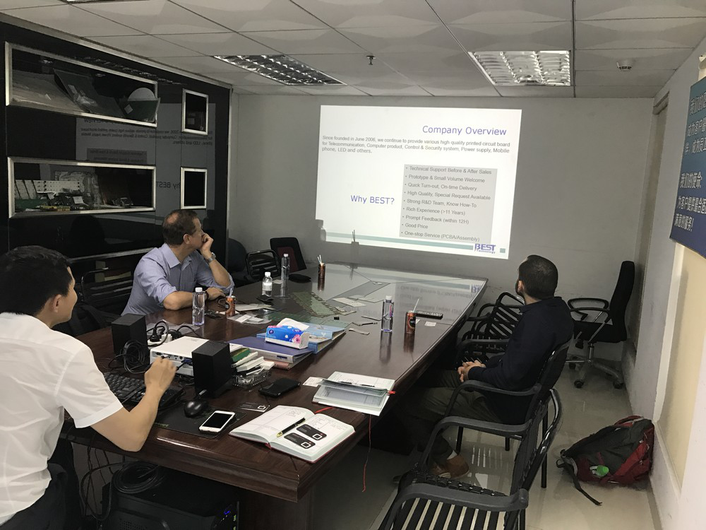
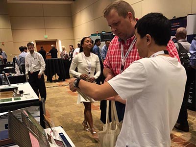
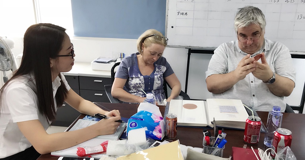
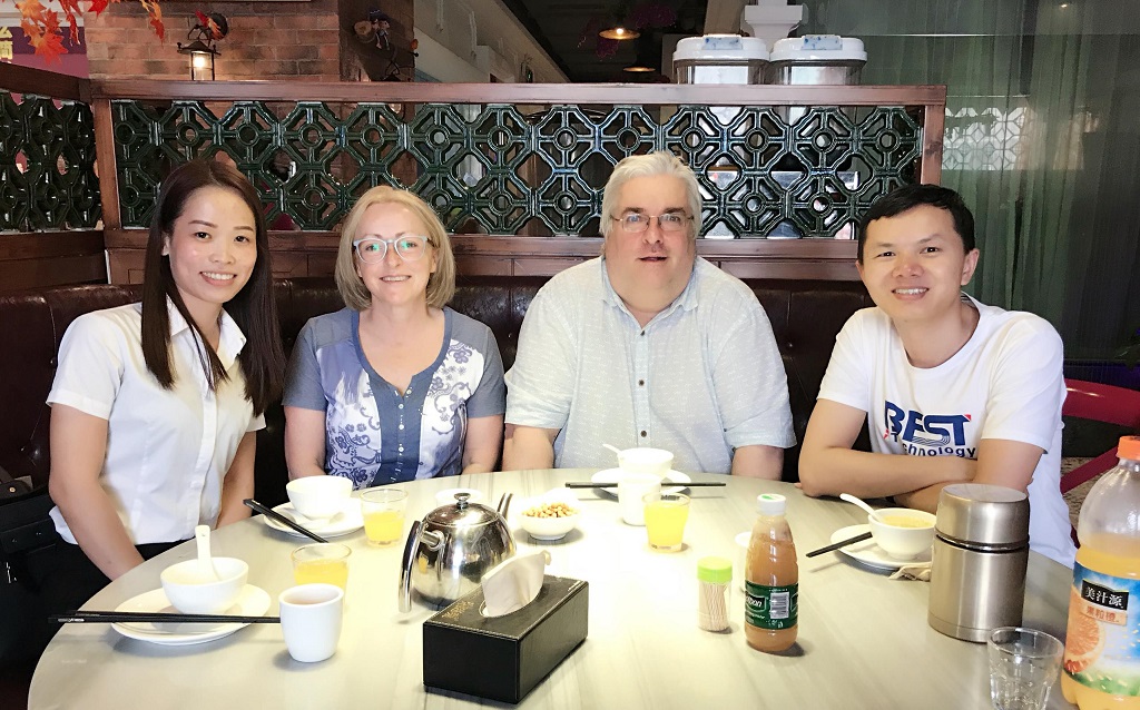
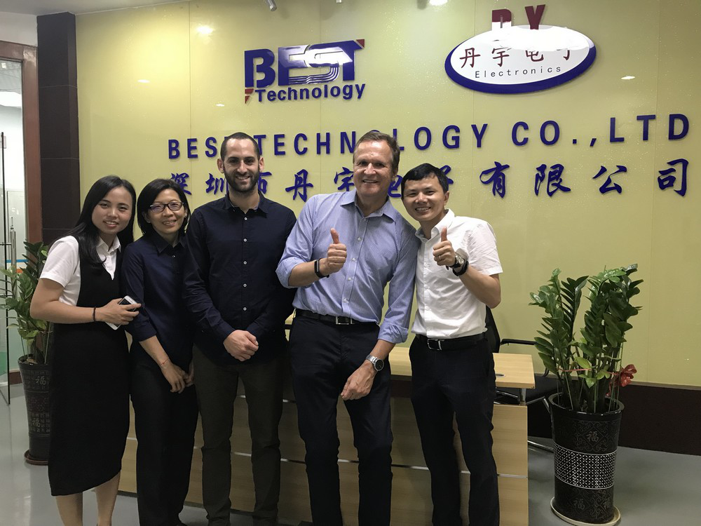
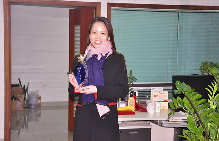
Providing customers with the most suitable products and the most satisfactory service is our mission. The high quality service of our company has attracted many customers to visit. On Aug. 9th, 2018, it was really our honor to have the nice American customers visiting Best Technology.

Taking a photo in Best Technology office
Picture1: Taking a photo in Best Technology office
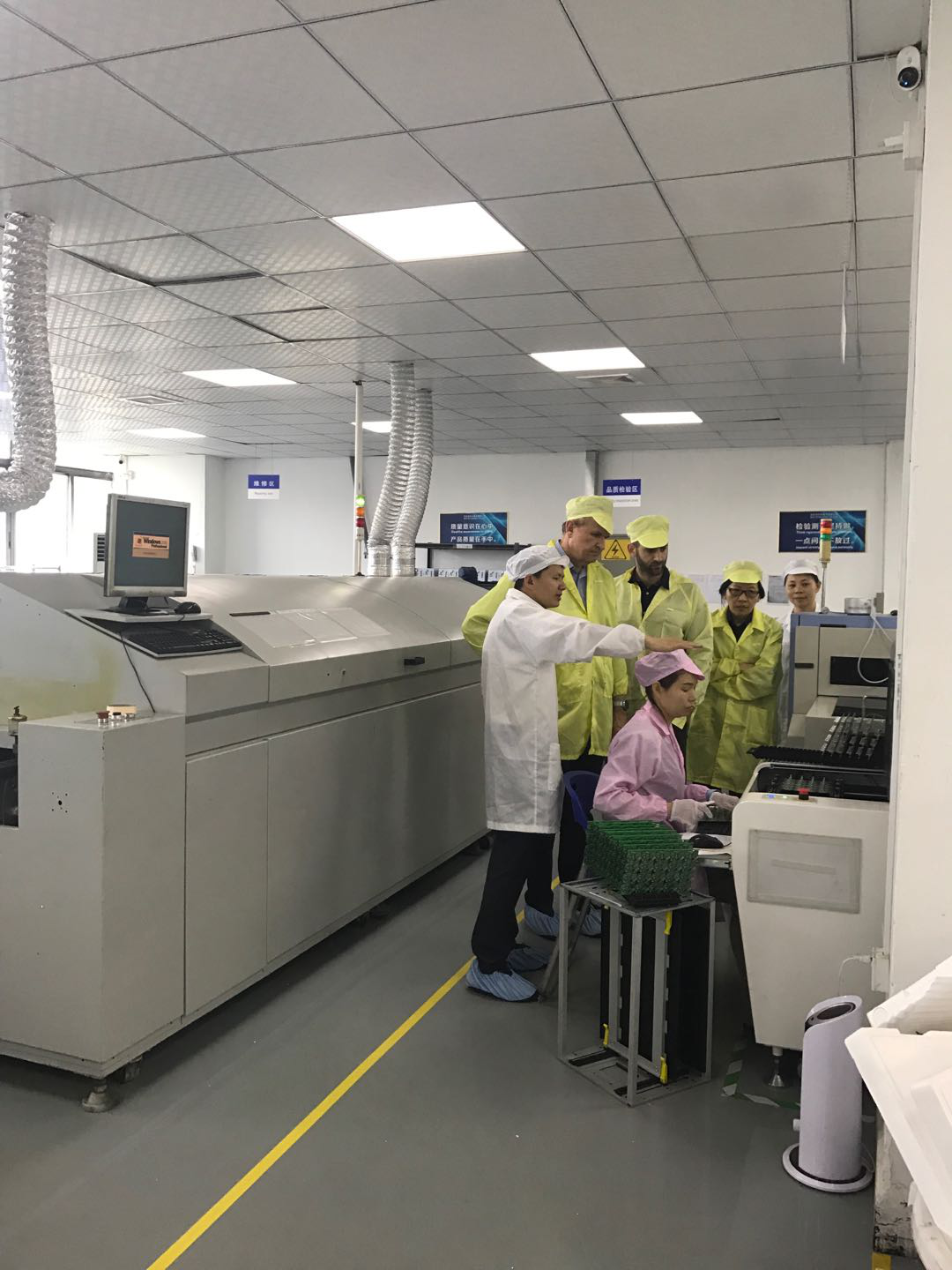
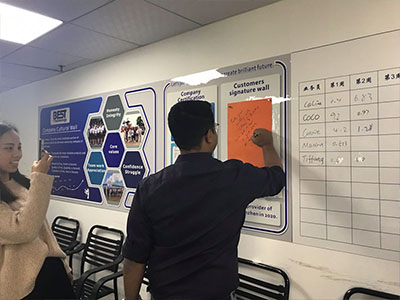
Visiting the drilling house
Picture2: Visiting the drilling house

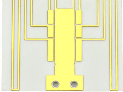
We have met each other before. The point to the meeting was to discuss the matters that something need to pay attention to cooperation in the follow-up. What’s more, they would like to get more information about our products, such as thick film ceramic PCB, thin film ceramic PCB and DCB Ceramic PCB.

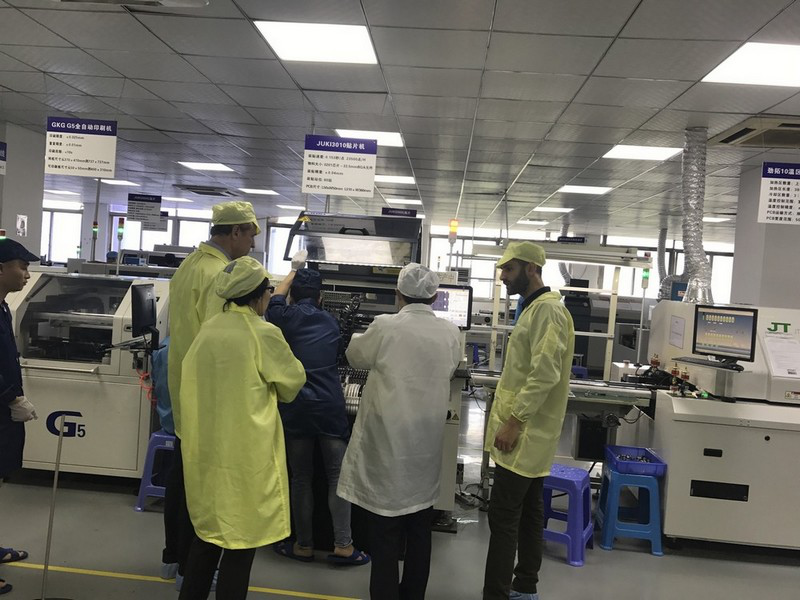
Board routing process
Picture3: Board routing process

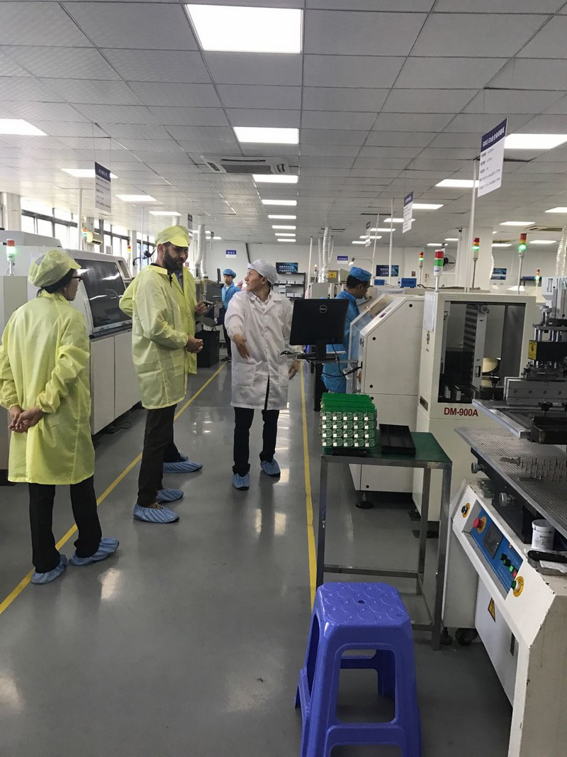
Meanwhile, the customers also wanted to visit our factory of printed circuit board to see the production process and capacity of the printed circuit board. So after the short meeting, we took the customers to visit the different workshops of production and explained the details that need to be paid attention to in each process of production.

  The customers were really satisfied with our services and looked forward to our next cooperation.

You may also like

Irish customer visit Best Technology on Aug. 28th, 2018
Wednesday, August 29th, 2018

On Aug. 28th, 2018, we had customers coming from Ireland. It is the first time that they have come to visit our company to see the samples. We talked about the current situation in UK and it will give our company more new chances to provide Circuit Boards to EU. Believe our Ceramic PCB will support them to develop more market in EU.

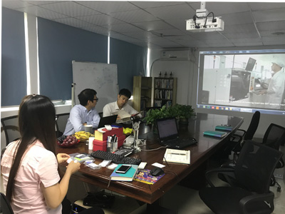
Customers see the samples in the meeting room

Customers see the samples in the meeting room

We also provide other kinds PCB to customers, such as Rigid-flex circuit, FPC, metal core PCB, Ceramic PCB , as well as some  special PCB,  Heavy copper PCB,  High Tg PCB,   PCB assembly  products.

After seeing the samples, we had a delicious lunch:

Having lunch with customers

Having lunch with customers

As a professional PCB vendor, Best Technology is always dedicated to provide the most suitable products and most satisfied services for customers. If you would like to know more information, please click here: https://www.bestpcbs.com/

You may also like

Welcome Israel Friends visit us
Friday, April 27th, 2018

In the morning of April 24th, 2018, our customer from Israel visited our company. They are very nice and easygoing.

Firstly we had a short meeting in our office to discuss some PCBA projects and component, also we invite them to see our company’s video, which they know more about our capability on PCB, Rigid-flex circuit, FPC, metal core PCB, Ceramic PCB and lead time for different circuit boards.


After that, we moved to our SMT plant, where is only 15 minutes far from our office.

In our PCB Assembly plant, we show customers PCBA (SMT) process: First put PCB on Auto-loading machine, then transfer to Auto-Solder-paste-printer, after than go to the next step of components pick & place by SMT machine, after visual checking, board will go throw to reflow oven, QC will check each piece of board after reflowing and then do function testing, or move to AOI process to make sure all components are on the correct position and direction, as well as X-ray testing for the boards with BGA.


Each step was monitor and operators are following up with the SOP, to make sure quality is always controlled, and customer are interesting in how we test the assembly boards using testing fixture.


Customer is very happy with our SMT procedure and become more confident in placing more circuit board and PCBA order with Best Technology. After the meeting, we have a quick but delicious Chinese lunch together. And we will visit that customer in the end of May and believe by that time, we can do more things together, as well as good memories with each other.

Appreciate again for their valuable time to visit us, that’s our great pleasure to have that forenoon with them. Look forward seeing them again in Israel in the end of May.

We always welcome customer to visit us, so that they can know about what we can make, not only providing various types of printed circuit board, but also always supporting customer best service with good price.


You may also like

Company PCB & SMT Video Online Now!
Sunday, October 25th, 2015

Good news! Our company Video of PCB & SMT was online now!  You can see our team member, facility, production capability (includes FR4 PCB, Metal Core PCB, Ceramic PCB, Flexible Circuit, SMT (PCBA), to see how we continue to improve ourselves, to provide best service to our customers.

Please watch the following video on YouTuBe if you cannot open the above video.

Remember Best Technology will be your best choice of printed circuit board, most reliable partner in China!

Welcome to contact us today for more inquiries of various circuit boards.

You may also like

What the Maximum Current the Thick Film Ceramic PCB can be Carried?
Tuesday, January 27th, 2015

A lot of customers ask us what the biggest current his circuit can be carried, or how can I got a 6 Amps trace? We believe most of engineer design the thick film ceramic PCB, he will consider that, so we share information bellowing and hope it’ll be helpful for you.

When you try to know current, you also need to know the watts of trace will be, and then need to know the power density of thick film ceramic PCB firstly. The power density for conductor itself should be limited to max 600 Watt/inch2 of conductor surface. And power density for an Al2O3 substrate should be limited to 8 Watts/in2 (for the total of all conductors on top of it).

If you have a Ag conductor line of 0.3inch long, 0.010 inch wide (=30 square (0.3/0.01)), the surface area is 0.3 x 0.01 = 0.003 in2. This means the carrying powder P is limited to 600 (power density) x 0.003 (area) = 1.8 watts.

Assume conductor resistivity is 6mOhm/sq/12.5um (material P/N: ESL9562), the resistance value R = 30 sq x 6mOhm = 0.18 ohm.

Power = I2 x R, or I2 =Power/R=1.8/0.18 = 10, so the carrying current limit I = 3.16 amps. Or in a short equation,

I (amps) = line width (inch) x (power density)1/2 / (sheet resistance, ohm) 1/2

  1. If the trace keep 0.3 inch long, but change width to 0.02inch, (=15 square (0.3/0.02), the surface area is 0.3 x 0.02 = 0.006 in2. This means the carrying powder P is limited to 600 (power density) x 0.006 (area) = 6 watts.
    And resistance value for that trace will be 15 square x 6mOhm = 0.09 ohm, and then 3.6/0.09= 40, I=6.325 amps.
  2. If the trace width keep 0.01inch, but change line to 0.6 inch long (=60 square (0.6/0.01), the surface area is 0.6 x 0.01 = 0.006 in2. This means the carrying powder P is the same as 6 watts. (600×0.006).
    But the resistance value for that trace will change to be 60 square x 6mOhm = 0.36 ohm, and then 3.6/0.36= 10, I=3.16 amps. So you can see, it’s no useful to change the trace line.

So if you want to have bigger current for thick film ceramic PCB, then you need to increase the width of trace.

Hope above is clear for everybody. Please leave your comments on that power density of thick film ceramic PCB.

You may also like

Bigger size of Ceramic PCB is Available Now!
Wednesday, December 10th, 2014

Good news! This month we have used a new machine which can print much bigger size of silver palladium, Gold palladium, and glass glaze on Thick Film Ceramic PCB.

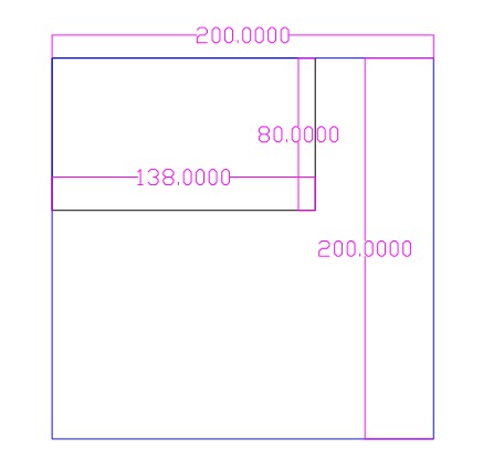
Currently the normal dimension in thick film Ceramic PCB is about 80 x 138mm and that size has already limited a lot of designs. You can’t put too much trace, PAD on such smaller size board, and the you have to use 2 layer, or 4 layers ceramic board to put more trace. And of course, that will increase a lot of cost definitely!

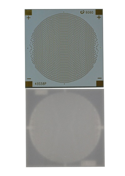
Now, we can make 200 x 200mm (8×8 inch). Thinking about the normal 80x138mm and you will find out this is an extreme improving! See bellowing pictures show the comparing!

Ceramic PCB size comparing

Ceramic PCB size comparing

So now you don’t need to worry about the size! You can design as big as you want!

And we are also continuing to adopt first-of-art machine and technology to make bigger size, higher quality Ceramic PCB!

Please contact us if you have more good idea, or suggestion about Ceramic PCB.


You may also like