LiDAR (Light Detection And Ranging, referred to as “LiDAR”) measurement is a system that integrates three technologies: laser, GPS (Global Positioning System), and IMU (Inertial Measurement Unit, inertial measurement unit), used to obtain data and Generate accurate DEMs (Digital Elevation Models). The combination of these three technologies can highly accurately locate the spot of the laser beam on the object, and the ranging accuracy can reach the centimeter level. The biggest advantage of lidar is accurate, fast, and efficient operation.

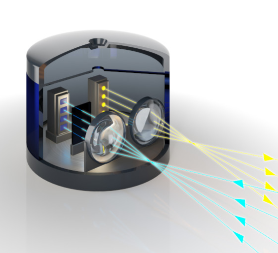
Lidar is currently widely used in the field of driverless cars and robots. It is known as the “eye” of a generalized robot. It is an active measurement device that measures the precise distance between an object and a sensor by emitting laser light.
As an indispensable sensor for L3 and above automatic driving, lidar has significantly improved the reliability of the automatic driving system with its excellent ranging capability, high angular resolution and sensitivity to ambient light, and has become the key to improving reliability. A key element of autonomous driving systems, but its application is constrained by cost and technical challenges.
In the past, lidar was difficult to apply to mass-produced vehicles due to its high cost. However, recently, with the continuous evolution of technology and market competition, the cost of lidar has gradually decreased, thereby accelerating its application in the field of autonomous driving.
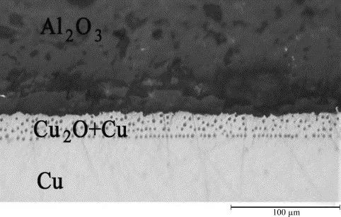
In this evolution process, the emergence of ceramic substrates has played a vital role in the breakthrough of lidar technology – 905nm wavelength lidar has become mainstream. Traditional materials such as FR-4 and FE-3 are difficult to meet the high heat dissipation requirements of lidar, while ceramic substrates rely on their excellent thermal conductivity. For example, the thermal conductivity of aluminum nitride ceramic substrates is as high as 200W/M.K. It effectively solves the heat dissipation problem and provides a guarantee for the stability and life of the lidar.
In lidar, the transmitter is one of the links with the highest value and the highest barriers. On the transmitter side, with the rise of China’s domestic industrial chain and the adjustment of the overall technical route of the industry, among them, 905nm VCSEL laser chips and other products have achieved breakthroughs in the market and become a hot topic in the industry.
The “heart” of the transmitter is the light source. Laser transmitter is the core component of laser technology, and its composition includes laser working medium, excitation source and resonant cavity. In this system, why choose a ceramic substrate as a component? The main reason lies in its unique advantages in heat dissipation. Especially for VCSEL (Vertical Cavity Surface Emitting Laser) chips, due to their low power conversion efficiency, the problem of heat dissipation is particularly prominent. The application of ceramic substrates has become the best choice to solve the problem of thermoelectric separation.
The ceramic substrate has excellent heat dissipation performance and can effectively conduct the heat generated inside the laser transmitter. The high thermal conductivity of the ceramic substrate allows it to efficiently conduct heat generated inside the lidar, preventing performance degradation due to overheating. In addition, ceramic materials have the advantages of high strength, hardness, thermal shock resistance, insulation, and chemical stability, which can further extend the service life of products, improve sensitivity, and enhance the response speed of lidar.
Ceramic substrates also enable high-density assembly, supporting miniaturization and integration of devices. Its stability ensures that the sensor signal is not distorted, and the matching with the thermal expansion coefficient of the chip ensures the reliability of the product in harsh environments such as high temperature, high vibration, and corrosion. In addition, the metal crystallization performance of the ceramic substrate is excellent, which ensures the stability of the circuit and further improves the quality control level of the lidar.
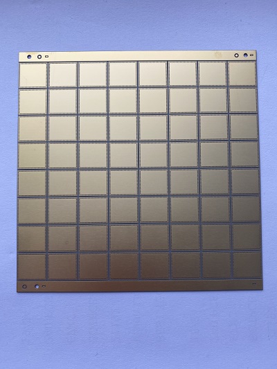
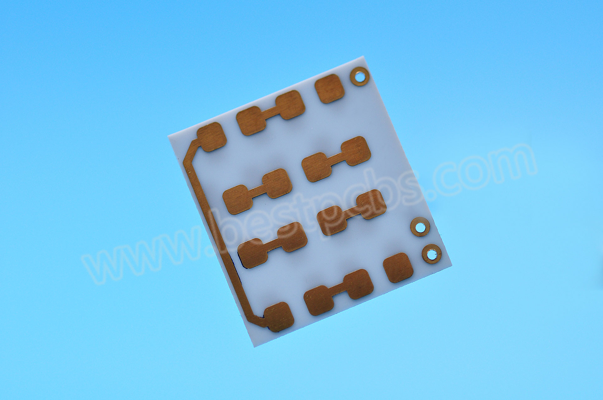
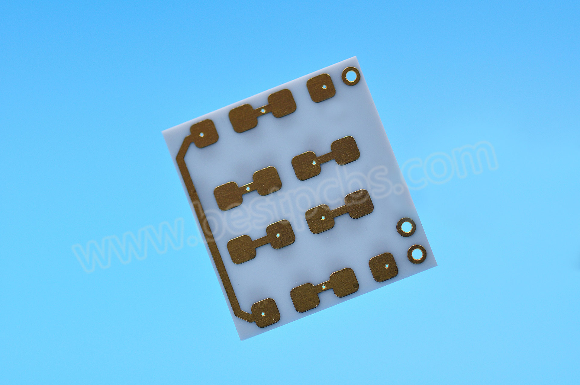
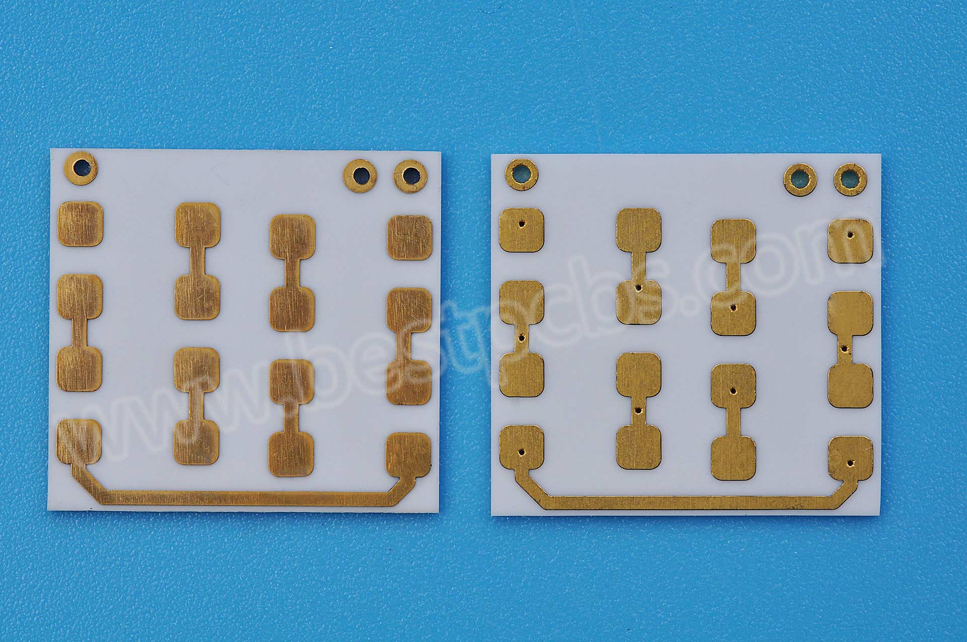
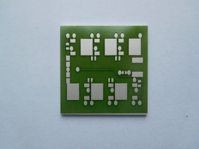
As a leading manufacturer of ceramic substrates, Best Technology provides a variety of ceramic substrates of different materials, including 96% alumina, 99% alumina, aluminum nitride, zirconia, silicon nitride, sapphire ceramic bases, etc. The heat dissipation properties of these different materials are different, such as aluminum nitride (AlN): thermal conductivity of 170-230 W/mK, silicon nitride (Si3N4): thermal conductivity of 20-80 W/mK, sapphire (Al2O3): thermal conductivity Coefficient 25-40W/mK.
Therefore, choosing a high-quality ceramic substrate not only helps to solve the problem of thermal and electrical separation of laser emitters, but also provides stable heat dissipation and electrical performance, providing reliable support for efficient operation and performance improvement of laser emitters. In the development of lidar technology, ceramic substrates play an increasingly important role, providing key support for performance breakthroughs and innovations in laser transmitters. We are witnessing a revolution in the auto industry brought about by China’s autonomous driving assistance systems.
If you are designing a ceramic PCB and seeking a reliable manufacturer, welcome to leave you message or contact us directly.