pcb
Home > Blog

Archive for the ‘FAQ’ Category

PCB Stencil: What is Stencil in PCB & How to Use PCB Stencil
Tuesday, February 18th, 2025

What is a Stencil in PCB?

A PCB stencil is a precision tool used in the process of assembling printed circuit boards. Its main function is to apply solder paste to the board in a controlled manner, ensuring the paste only reaches the pads where components will be mounted. By creating uniform paste deposits, the stencil facilitates the correct soldering of components during the assembly process, contributing significantly to the quality and reliability of the final product.

PCB Stencil: What is Stencil in PCB & How to Use PCB Stencil

What Does a Stencil Do?

A PCB stencil plays several crucial roles in the PCB assembly process, including:

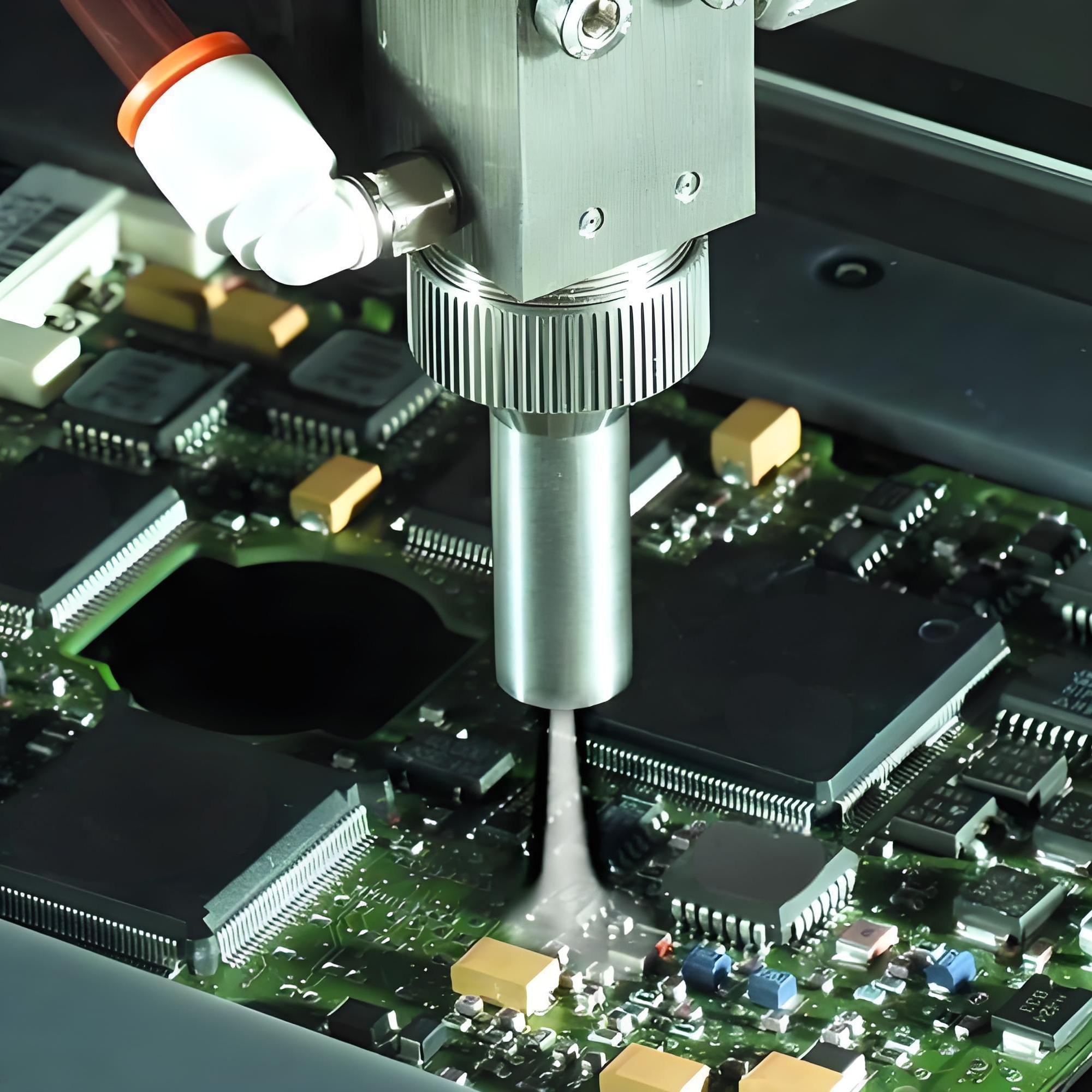
1. Applies Solder Paste: The primary function of a stencil is to accurately apply solder paste to the PCB. The paste is deposited onto the pads of the PCB through the openings in the stencil, ensuring the right amount of paste is used for each component.

2. Improve Precision: By using a stencil, manufacturers can achieve highly precise solder paste placement. This is especially important for fine-pitch components, where precision is key to avoiding defects like bridging or insufficient solder.

3. High Efficiency: Stencils speed up the solder paste application process, making it more efficient than manual paste application. This is particularly beneficial in high-volume manufacturing, where consistency and speed are vital.

4. Reduces Human Error: Using a stencil minimizes the chances of human error in solder paste application. This leads to more consistent and reliable results, reducing the likelihood of defects in the final product.

5. Facilitates High-Volume Production: Stencils are essential for mass production, allowing manufacturers to quickly and efficiently apply paste across multiple PCBs with high consistency.

6. Improves Reflow Soldering: With the right amount of solder paste applied, the stencil helps ensure that the reflow soldering process is carried out effectively, leading to strong and durable solder joints.

What is a PCB Stencil Consist of?

A PCB stencil consists of several crucial components that work together to ensure precise solder paste application. These elements include:

1. Frame

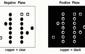
The frame is essential for holding the stencil in place during the application process. It is categorized into movable frames and fixed frames. The movable frame attaches the steel plate directly to the frame, allowing the template to be reused. On the other hand, the fixed frame uses adhesive to attach the wire mesh to the formwork. For optimal performance, a strong frame with uniform steel tension—typically between 35 and 48 N/cm²—is preferred. The normal fixed frame tension is between 35 N to 42 N, ensuring stability and accuracy.

2. Sheet Plates

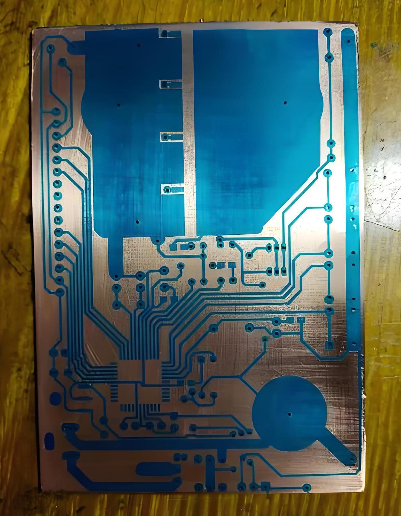
High-quality stainless steel plates such as 301/304 stainless steel are commonly used because they offer excellent mechanical properties, significantly increasing the service life of the stencil. Other materials such as copper plates, nickel alloy, and polyester may also be used, depending on the specific application requirements.

3. Mesh

The mesh is used to fix the steel plates and formwork in place. There are two main types of mesh: stainless steel mesh and polymer polyester mesh. Stainless steel mesh is typically around 100 mesh and ensures stable tension, but it can deform and lose tension over time. Polyester mesh, on the other hand, is made from an organic fabric that doesn’t easily deform and has a longer service life, making it a more durable option for long-term use.

4. Adhesive (Glue)

The glue used in PCB stencils serves as the binding material that attaches the trellis frame to the steel sheet. It is an essential part of maintaining the integrity and stability of the stencil. The adhesive used needs to provide strong adhesion and be able to withstand heavy cleaning with various plate cleaners without losing its effectiveness.

Together, these components—frame, sheet, mesh, and glue—combine to form a PCB stencil that ensures accurate, consistent, and efficient solder paste application during the PCB assembly process.

What Are the Different Types of Stencils?

There are various types of PCB stencils, each designed for specific applications and production requirements:

  • Laser-Cut Stencils: These are the most accurate and commonly used type. Laser cutting provides high precision, making these stencils perfect for fine-pitch components or designs with intricate details.
  • Etched Stencils: Etching is an older method but still used for simpler projects. Though less precise than laser-cut stencils, etched stencils are still valuable for projects where absolute precision is not as critical.
  • 3D Printed Stencils: 3D printing technology has opened up a new avenue for creating PCB stencils. This method is ideal for low-volume or prototype PCB assembly, offering flexibility and faster turnaround times for custom designs.
  • DIY Stencils: For hobbyists or small-scale production, DIY methods using materials like adhesive-backed foil or plastic sheets can be used to create simple stencils. These are cost-effective but come with trade-offs in precision and durability.
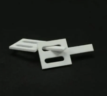
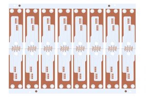
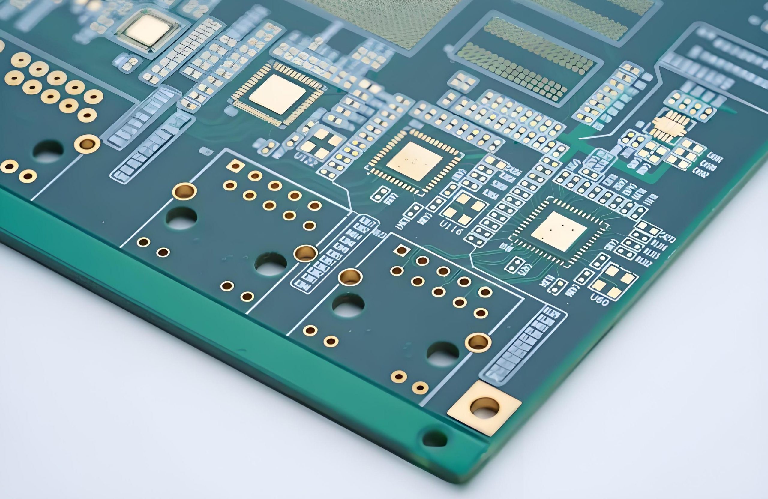
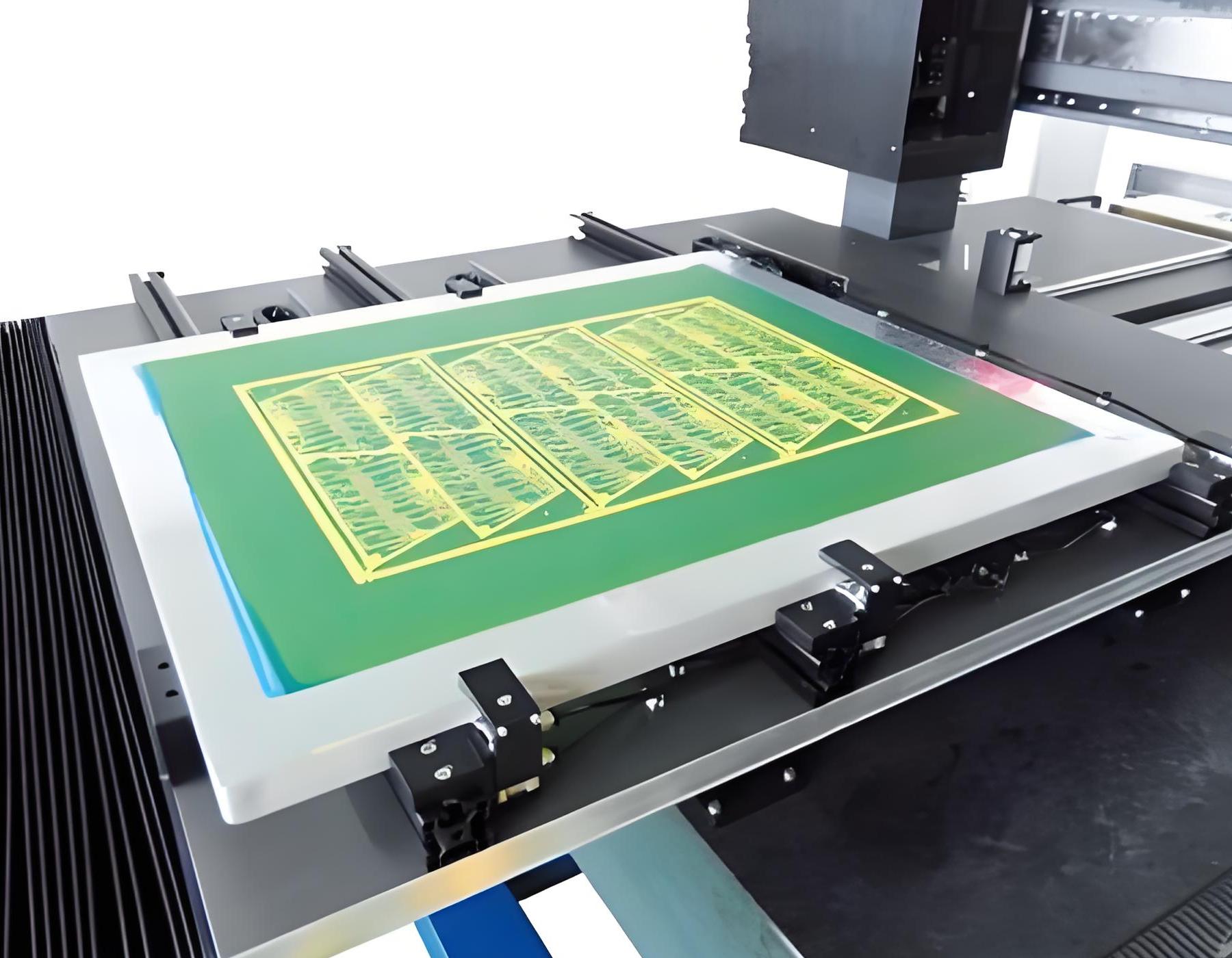
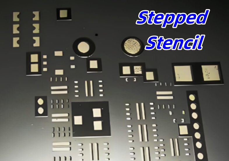
  • Stepped Stencil: A stepped stencil features varying thicknesses across different areas of the stencil. These thickness changes, or “steps,” allow the stencil to deposit different amounts of solder paste for different components on the same PCB. Stepped stencils are particularly useful when there is a mix of fine-pitch components and larger, more spaced-out components on the same board. Below is a typical photo of stepped stencil.
PCB Stencil: What is Stencil in PCB & How to Use PCB Stencil

PCB Stencil HS Code

The HS code for PCB stencils is 7314490000.

This code is specifically used for steel product, which includes PCB stencils used in the manufacturing process. It’s important to use the correct HS code for shipping and customs purposes to ensure smooth international transactions.

Warm Notice:

It’s always advisable to check with your local customs authority for any updates or specific requirements based on your region or the material type.

PCB Stencil Thickness

The thickness of a PCB stencil is an important factor in ensuring the correct amount of solder paste is applied. Generally, the stencil thickness ranges between 0.08 mm to 0.20 mm.

And it depends on the smallest spacing of the components on the PCB.

  • For BGAs or ICs with a 0.35mm pitch, a stencil of 0.08mm or thinner is recommended. If the entire PCB features such fine-pitch components, a stencil thickness of 0.06mm or even 0.05mm is more suitable.
  • For BGAs or ICs with a pitch of 0.4mm or greater, a 0.1mm thick stencil is acceptable. In some cases, for BGAs with a slightly larger pitch, a 0.08mm thick stencil may also be considered. When dealing with BGAs or ICs that have a pitch of 0.5mm or more, a 0.12mm thick stencil is the optimal choice.

Moreover, the stencil thickness affects both its suitability and lifespan. Thinner stencils, like 0.08mm, are ideal for high-precision solder points. On the other hand, thicker stencils, such as 0.12mm, are better for scenarios where component spacing is larger, ensuring greater stability and strength.

PCB Stencil Material

The material selection for PCB stencils influences the overall performance and durability of the tool. Common materials include:

  • Stainless Steel: As the most popular option, stainless steel provides the necessary durability, resistance to corrosion, and ease of cleaning required for frequent use in high-precision environments.
  • Nickel: While not as common as stainless steel, nickel-based stencils are valued for their flexibility and wear resistance. They are often chosen for specific applications requiring extra resilience.

The material selected must align with the type of PCB being produced, ensuring long-term effectiveness.

How to Make a PCB Stencil?

Creating a PCB stencil requires both precision and attention to detail. The process typically involves:

1. Designing the Stencil

    The stencil design is created based on the PCB layout, ensuring the paste is applied to the correct pads.

    2. Selecting the Material

    Choose either stainless steel or nickel, depending on the project requirements.

    3. Cutting or Etching the Design

    For laser-cut stencils, a laser cutter is used to cut out the design with high precision. Etched stencils use chemical etching to create the openings.

    4. Testing the Stencil

    After the stencil is manufactured, it is tested to ensure that it meets the design specifications and can transfer solder paste accurately.

    How Do You Solder a PCB with Stencils?

    Soldering a PCB with a stencil involves several steps:

    1. Place the PCB: The PCB is positioned on a flat surface or assembly board.

    2. Align the Stencil: The PCB stencil is carefully placed on top of the PCB, ensuring that the openings align with the pads.

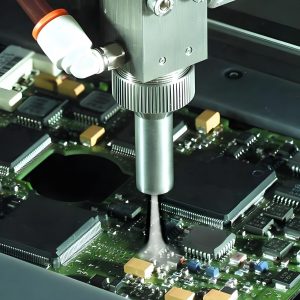
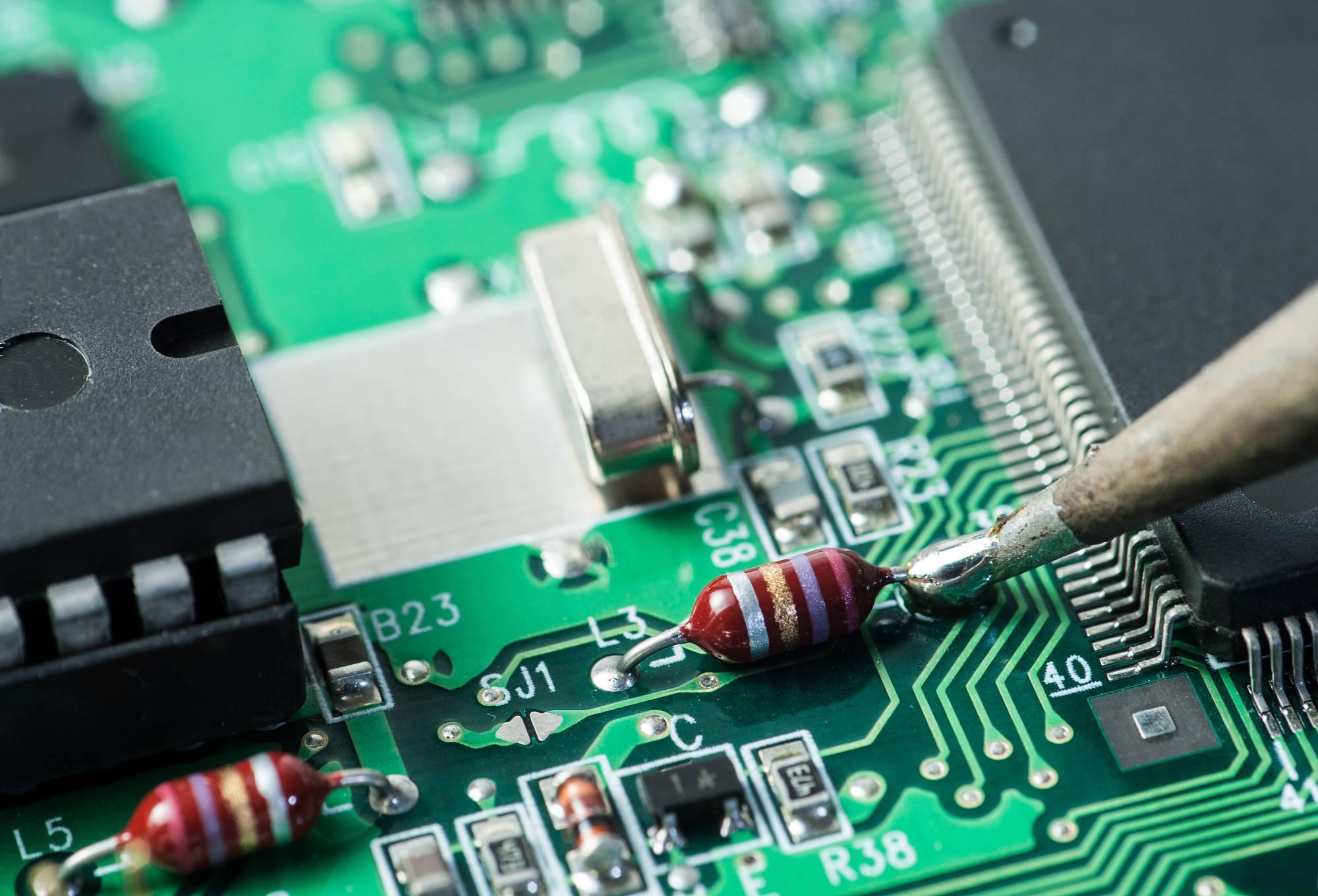
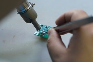
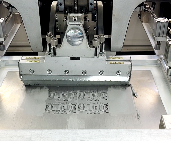
    3. Apply Solder Paste: Solder paste is applied over the stencil using a squeegee or automated machine, filling the openings on the stencil.

    PCB Stencil: What is Stencil in PCB & How to Use PCB Stencil

    4. Remove the Stencil: The stencil is carefully lifted off, leaving solder paste on the pads.

    5. Place Components: Components are placed onto the paste before the board is sent through a reflow oven, where the paste melts and creates strong, reliable solder joints.

    PCB Stencil: What is Stencil in PCB & How to Use PCB Stencil

    How Much Does a PCB Stencil Cost?

    The cost of a PCB stencil varies depending on the material, thickness, design complexity, and order volume. On average:

    • Laser-cut stencils can range from $50 to $200 for single units, with bulk orders offering reduced prices.
    • Etched stencils tend to be more affordable, typically priced around $30 to $100 depending on size and complexity.
    • 3D printed stencils are generally more expensive due to the novelty of the technology, with prices starting around $100 for small projects.

    For high-volume production, manufacturers often work with suppliers to negotiate bulk pricing.

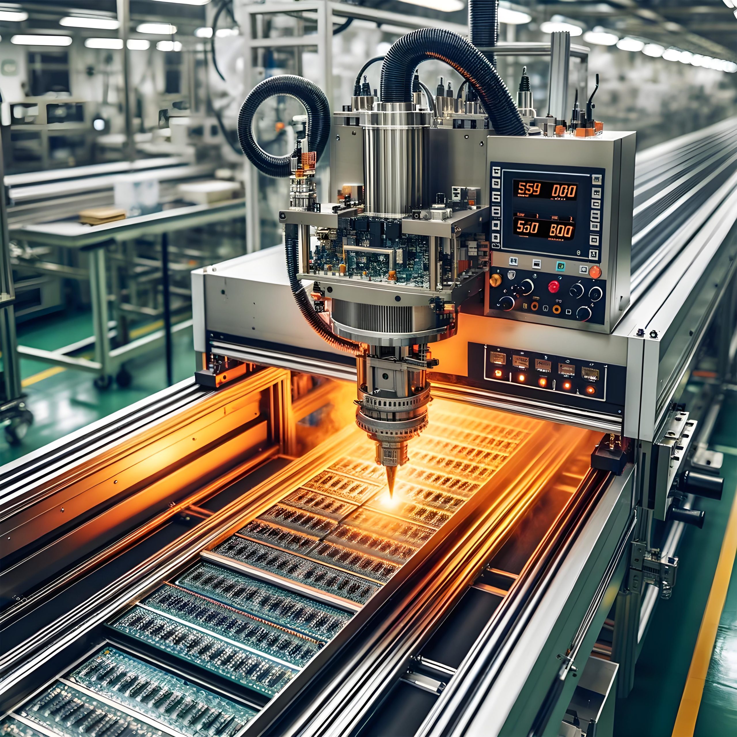
    Stencil PCB Printers vs. PCB Stencils

    While PCB stencils manually apply solder paste, PCB stencil printers are automated machines designed for mass production. The printer ensures the paste is applied consistently and accurately across the entire board, which is ideal for high-volume manufacturing.

    The main difference is in automation. Stencil printers remove the need for manual labor, reducing the chance of human error and speeding up production time. On the other hand, manual PCB stencils are still effective for small-scale or custom PCB production, though they may require more time and care.

    PCB Stencil Manufacturer – Best Technology

    At Best Technology, we specialize in producing high-quality PCB stencils designed to meet the most demanding needs of the PCB assembly industry. With over 18 years of experience, we provide custom stencil solutions, ensuring your production runs smoothly and efficiently.

    Whether you’re looking for a laser-cut, etched, or 3D printed stencil, our team offers precision and flexibility to help bring your designs to life. Choose Best Technology for your PCB stencil needs and experience the difference in quality and service. For more information, e-mail us at sales@bestpcbs.com.

    You may also like

    PCB Protection: What is PCB coating?
    Tuesday, February 18th, 2025

    PCB coating is a layer of special material applied on the surface of PCB to protect the circuit board from environmental factors (such as moisture, dust, chemical corrosion, etc.) while improving its electrical insulation, welding performance and mechanical strength. Common coating types include organic coating, metal plating, conformal coating, etc., which are applied by spraying, dipping or brushing.

    PCB Protection: What is PCB coating?

    What is conformal coating on pcb?

    Conformal coating is a protective layer applied to a PCB to shield the board’s components from external contaminants like dust, moisture, and chemicals.

    Unlike encapsulation, which surrounds the entire assembly, conformal coating is a thin, flexible layer that conforms to the shape of the PCB and its components. The coating allows the PCB to remain functional while also protecting it from environmental stresses.

    The purpose of conformal coating is to enhance the reliability and longevity of PCBs by protecting them from elements that could cause short circuits, corrosion, or other types of damage.

    It is particularly critical in industries where the PCB is exposed to harsh environments or where the failure of a PCB could have severe consequences.

    Why conformal coating is used in pcb?

    There are several reasons why conformal coating is essential for PCBs:

    • Protection from Moisture: Moisture is one of the biggest threats to PCBs. The coating provides a moisture-resistant barrier, reducing the risk of corrosion and electrical shorts.
    PCB Protection: What is PCB coating?
    • Dust and Contaminant Shielding: Dust, dirt, and other environmental contaminants can easily find their way onto uncoated PCBs. A conformal coating prevents this by creating a physical barrier.
    • Chemical Resistance: Many industrial environments expose PCBs to chemicals, oils, and solvents. A good conformal coating can offer protection against these substances, preserving the integrity of the PCB.
    • Electrical Insulation: In certain cases, conformal coatings help isolate electrical components from one another, preventing unwanted connections or short circuits.
    • Thermal Resistance: In some instances, conformal coatings can help dissipate heat, allowing the PCB to operate more efficiently in high-temperature environments.

    In summary, PCB coatings ensure better reliability, enhanced performance, and longer lifespan, especially in medical, automotive, and aerospace sectors.

    Can conformal coating be removed?

    Yes, conformal coating can be removed, though the process is often delicate and requires careful handling.

    PCB coating removal is generally done when there’s a need for repair, modification, or redesign of the PCB. However, the removal process must be approached with caution to prevent damaging the underlying components.

    Some coating removal techniques include using:

    • Chemical Strippers: These are special solvents designed to break down and dissolve the coating.
    • Mechanical Methods: Using tools like abrasive pads or brushes, the coating can be scrubbed off.
    • Heat Application: For certain coatings, heat guns or infrared ovens can soften the coating, making it easier to remove.

    Each method should be selected based on the type of coating and the sensitivity of the PCB components.

    How to remove conformal coating from pcb?

    • Choose the Right Method: Select a removal technique based on the type of coating and the nature of the PCB.
    • Use Protective Gear: Always wear gloves, goggles, and a mask to avoid exposure to chemicals and solvents.
    • Apply Solvent: If using a chemical stripper, apply it carefully to the PCB using a brush or cloth. Allow the solution to sit for a few minutes to break down the coating.
    • Scrub Off the Coating: Use a soft brush or sponge to scrub the coating off. Avoid using hard bristles that could damage the PCB.
    • Rinse and Dry: Once the coating has been removed, rinse the PCB with water or alcohol to remove any chemical residues. Allow the PCB to dry completely before reapplying a new coating or proceeding with repairs.

    What is the best coating for PCB?

    The best coating for PCB depends on various factors, including the environment in which the PCB will operate, the level of protection needed, and the specific requirements of the project.

    • Acrylic Coating: This is one of the most common PCB coatings due to its excellent moisture resistance, ease of application, and good overall protection. It is clear, which makes it ideal for applications where visual inspection is needed.
    • Silicone Coating: Known for its flexibility and high-temperature resistance, silicone coating is often used in PCBs that will be exposed to high heat or thermal cycling.
    PCB Protection: What is PCB coating?
    • Polyurethane Coating: Offering high durability and excellent resistance to environmental factors, polyurethane coating is ideal for industrial applications that require both moisture and chemical resistance.
    • Epoxy Coating: Epoxy coatings provide strong protection against mechanical wear and harsh environments but are less flexible than other coatings.
    • Parylene Coating: Parylene is a highly effective coating for PCBs, offering protection from chemicals and moisture while maintaining a very thin and uniform layer. It is commonly used in medical and aerospace applications.

    Each type has its advantages, so it’s essential to select the one that best fits your needs.

    What is the cheapest PCB finish?

    When it comes to PCB finishes, the cost can vary widely depending on the type of finish chosen.

    Acrylic coatings are often considered among the most affordable options, providing good protection for general applications.

    However, when specific environmental conditions require more advanced coatings (like Parylene or silicone), the cost can be higher.

    Opting for a lower-quality coating may result in increased wear and tear or reduced protection, leading to failures over time.

    How to measure conformal coating thickness?

    Too thick a coating can cause unwanted stress on components, while too thin a layer might not provide sufficient protection.

    The most common methods for measuring coating thickness are:

    • Micrometers: Special digital micrometers can be used to measure the thickness of the coating with great precision.
    • Ultrasonic Testing: This non-destructive method uses sound waves to measure the thickness of coatings.
    • Coating Thickness Gauges: These handheld tools use electromagnetic induction or eddy current technology to measure coating thickness quickly and accurately.

    It’s vital to measure coating thickness regularly during the application process to maintain consistent protection across the entire PCB.

    What are the drawbacks of conformal coating?

    While conformal coatings offer numerous benefits, there are some drawbacks to consider:

    • Limited Protection for Physical Damage: While they protect against moisture and contaminants, coatings don’t provide protection against physical impacts or harsh mechanical stresses.
    • Coating Removal Complexity: Removing conformal coatings can be tricky and requires specialized techniques and tools.
    • Potential for Uneven Coating: If the coating process is not executed correctly, it could result in areas where the coating is too thick or thin, leading to reduced protection or malfunctioning.
    • Increased Component Stresses: Some coatings, especially those that are too thick or rigid, can put additional strain on the components, leading to potential damage over time.

    Despite these drawbacks, the benefits of conformal coatings often outweigh the disadvantages, especially when dealing with sensitive electronics exposed to harsh environments.

    How do you apply conformal coating to PCB?

    Applying conformal coating to PCBs can be done through several methods, including:

    • Spraying: Spray applications are one of the most common methods for applying conformal coatings. It provides even coverage and is suitable for large-scale production.
    PCB Protection: What is PCB coating?
    • Dipping: In this method, the entire PCB is dipped into a bath of conformal coating material, allowing it to coat the board evenly.
    • Brushing: For smaller batches or repairs, brushing is a viable method.
    • Selective Coating Machines: These machines can apply conformal coatings only to the areas of the PCB that need protection, minimizing wastage.

    Each method has its benefits, and the choice depends on the specific project and production needs.

    Conclusion:

    PCB coating is an essential protective measure that ensures PCBs can withstand environmental challenges while maintaining functionality.

    At Best Technology, Our experienced engineers will help you choose the best solution for your project, ensuring your PCBs are protected and reliable. For more information, contact us at sales@bestpcbs.com

    You may also like

    Let you know what are electron devices and circuits
    Tuesday, February 18th, 2025

    What are electron devices and circuits? Electronic devices are basic components that realize signal processing and control functions, such as resistors and capacitors; circuits are systems formed by connecting these devices through conductive paths to complete specific functions. PCB is a physical platform that carries and connects electronic devices and is the foundation of modern electronic devices.

    Let you know what are electron devices and circuits

    What are electronic devices and circuits?

    At their core, electronic devices and circuits refer to components and systems that use electricity to perform specific tasks. Electronic devices are typically powered by electrical energy, and they rely on electronic circuits to direct and manage that energy.

    Electronic circuits are pathways made from various components like resistors, capacitors, diodes, and transistors that regulate the flow of electric current.

    When these components are connected in the right way, they allow an electronic device to work as intended. In essence, electronic devices are powered by circuits that control and manipulate electrical signals.

    The PCB inside your laptop connects different electronic components, allowing your computer to process data and interact with the user.

    What is considered an electronic device?

    Electronic devices are any tools or gadgets that use electrical energy to function. These devices rely on electronic circuits to operate and perform various functions, ranging from simple tasks to complex operations.

    • Smartphones and Tablets: These handheld devices contain a variety of electronic circuits that allow them to perform tasks like communication, entertainment, and productivity.
    • Computers: Laptops and desktops are complex electronic devices that include hundreds of electronic circuits working together to execute a wide range of functions.
    • Medical Devices: Devices like pacemakers, insulin pumps, and blood pressure monitors depend on electronic circuits to monitor and regulate various bodily functions.
    • Home Appliances: Everyday appliances such as refrigerators, air conditioners, and washing machines all rely on electronic circuits for automation and efficiency.

    These examples show that electronic devices vary greatly in function, but they all share one thing in common: they rely on electronic circuits to work.

    How to study electronic devices and circuits?

    Understanding electronic devices and circuits requires a combination of theory and hands-on learning. Here’s how to get started:

    • Learn the Basics: Start by understanding the fundamental components of electronic circuits like resistors, capacitors, transistors, and diodes.
    Let you know what are electron devices and circuits
    • Circuit Theory: To design and analyze circuits, this includes concepts like Ohm’s Law, Kirchhoff’s Laws, and understanding voltage, current, and resistance.
    • Hands-On Practice: Use a breadboard and other tools to build circuits.
    • Simulation Tools: Software like LTSpice or Multisim allows you to simulate circuits before physically building them.
    • Learn PCB Design: PCBs are at the heart of most electronic devices. Understanding how to design and manufacture PCBs is crucial for working with electronic circuits in real-world applications.

    What is the most basic circuit?

    The most basic circuit consists of three essential components: a power source, a load, and a conductor. This simple combination forms what is known as a series circuit.

    • Power Source: Provides the necessary electrical energy. In most cases, this could be a battery or a power supply.
    • Load: This is the component that consumes the electrical energy. A simple example is a light bulb that glows when connected to a circuit.
    • Conductor: The path through which electricity flows. Typically, wires or traces on a PCB are used as conductors.

    In a basic circuit, the power source sends current through the conductor, which powers the load. If any part of the circuit is broken, the current can no longer flow, and the circuit will not function.

    What are the basic types of circuits?

    Circuits can be divided into two main categories: series circuits and parallel circuits.

    • Series Circuits: In a series circuit, components are connected end-to-end, so the current flows through each component one after the other. The total resistance in the circuit is the sum of the individual resistances. If one component fails, the entire circuit is interrupted.
    Let you know what are electron devices and circuits
    • Parallel Circuits: In a parallel circuit, components are connected across the same two points, allowing the current to flow through multiple paths. If one path fails, the other paths will continue to function.

    Both types of circuits are essential in the design of electronic devices and circuits, and each has its specific applications depending on the device’s needs.

    What is the difference between circuits and devices?

    Circuits refer to the interconnected electrical components that manage the flow of electric current, while devices are the finished products that rely on those circuits to perform specific tasks.

    Circuits are made up of components such as resistors, capacitors, diodes, and transistors that interact to control and direct electrical energy.

    Devices, on the other hand, use these circuits to perform particular functions. A smartphone, for example, is a device that contains electronic circuits responsible for signal processing, battery management, and touch interaction.

    In short, circuits form the foundation of devices, but devices are what provide tangible functionality to users.

    What are the examples of electrical and electronic devices?

    Both electrical devices and electronic devices are widely used across different industries and everyday life. Let’s take a look at some examples of each:

    Electrical Devices: These include simple devices that convert electrical energy into other forms of energy, such as:

    • Electric fans
    • Heaters
    • Toasters

    Electronic Devices: These devices control electrical energy to perform more complex tasks, often involving signal processing, such as:

    Let you know what are electron devices and circuits
    • Smartphones
    • Computers
    • Medical devices (like ECG monitors)
    • TVs and radios

    Conclusion:

    When it comes to electronic devices and circuits, whether you are designing PCBs for smartphones, medical devices, or any other application, it is essential to have a good grasp of circuit theory and practical design techniques. At Best Technology, we specialize in providing top-quality PCBs for all your electronic device needs.

    For more information or to discuss your PCB requirements, please contact us at sales@bestpcbs.com

    You may also like

    PCB soldering process: What is the PCB soldering temp?
    Monday, February 17th, 2025

    PCB soldering temp varies due to different soldering processes and materials. Manual soldering temperature is generally between 300℃ and 350℃; wave soldering temperature is usually between 245℃ and 265℃; reflow zone temperature of reflow soldering is generally between 210℃ and 240℃. The lead-free soldering standard is 260℃±5℃, while the lead soldering standard is 230℃±5℃.

    PCB soldering process: What is the PCB soldering temp?

    What is the best soldering temperature for PCB?

    The ideal soldering temp depends on the type of solder used. Most lead-based solders melt at around 183°C (361°F), while lead-free solders require about 217-227°C (423-441°F).

    For manual soldering, a soldering iron temperature of 300-350°C (572-662°F) works well for most applications. Using a temperature-controlled soldering iron helps maintain precision.

    For automated soldering, such as wave or reflow soldering, temperature profiles are more complex. A gradual heating and cooling process ensures strong and reliable joints.

    Do you need flux to solder PCB?

    Yes, flux is essential. It removes oxidation, allowing solder to flow smoothly and bond properly. Without flux, solder may form weak or unreliable joints.

    Most solder wires have flux inside, but extra flux may be needed for complex PCB assemblies. For surface-mount devices (SMDs), a no-clean or rosin flux is commonly used.

    Using the right flux improves soldering efficiency and enhances the durability of the connections.

    What temperature does PCB solder reflow at?

    Reflow soldering is used for SMD assembly. It follows a controlled temperature profile to melt solder paste and bond components.

    PCB soldering process: What is the PCB soldering temp?

    A typical lead-free reflow profile includes:

    • Preheat: 150-200°C (302-392°F)
    • Soak: 200-217°C (392-423°F)
    • Reflow peak: 230-250°C (446-482°F)
    • Cooling: Gradual cooling to below 180°C (356°F)

    Lead-based solder requires lower peak temperatures, around 215-225°C (419-437°F).

    What temperature do you solder header pins to PCB?

    Header pins require a stable temperature between 320-350°C (608-662°F) for effective soldering.

    Using a lower temperature can result in cold joints. Higher temperatures may damage the plastic housing or PCB pads. A controlled approach ensures strong electrical and mechanical connections.

    Flux application also helps the solder flow better, improving joint quality.

    What temperature is flexible PCB soldering?

    Flexible PCBs (FPCs) are heat-sensitive. Excessive heat can damage the substrate. A controlled soldering temperature of 280-320°C (536-608°F) works best.

    For reflow soldering, a peak temperature of 230-245°C (446-473°F) is common. Careful handling and gradual heating prevent warping or delamination.

    Low-temperature solder pastes can also be used to reduce thermal stress on flex circuits.

    What temperature is SMD soldering?

    SMD soldering involves reflow, hot air, or manual soldering techniques. The temperature depends on the method used:

    • Reflow soldering: 230-250°C (446-482°F) peak temperature.
    • Hot air rework: 280-350°C (536-662°F) depending on component size.
    • Manual soldering: 300-350°C (572-662°F) with a fine-tip iron.

    Precise temperature control is critical to avoid thermal damage to small SMD components.

    What temperature should SMT soldering be?

    Surface-mount technology (SMT) soldering mainly relies on reflow soldering, where temperature must be carefully controlled.

    PCB soldering process: What is the PCB soldering temp?

    A standard SMT soldering profile includes:

    • Preheat: 150-180°C (302-356°F)
    • Soak: 180-220°C (356-428°F)
    • Peak: 230-250°C (446-482°F) for lead-free solder
    • Cooling: Gradual cooling to prevent thermal stress

    SMT soldering ensures high precision and reliability, making it the preferred method for modern PCB assembly.

    What wattage for pcb soldering?

    Soldering iron wattage impacts performance. For PCB work, 30-60W irons are ideal.

    • 30W-40W: Suitable for fine soldering tasks.
    • 50W-60W: Best for general PCB soldering, including through-hole and SMD.
    • Above 60W: Needed for heavy-duty tasks, like soldering large connectors.

    A temperature-controlled soldering station provides better accuracy and prevents overheating.

    What is the temperature range for pcb soldering process?

    The full temperature range for PCB soldering varies by method:

    PCB soldering process: What is the PCB soldering temp?
    • Manual soldering: 300-350°C (572-662°F)
    • Wave soldering: 245-265°C (473-509°F)
    • Reflow soldering: 230-250°C (446-482°F)
    • Hot air rework: 280-350°C (536-662°F)

    Different materials and components may require adjustments. Following the right temperature range ensures better quality and durability.

    Conclusion:

    Soldering temp is critical for PCB assembly. The right temperature ensures strong, reliable joints while preventing component damage.Each soldering method requires specific temperature settings. Whether manual soldering, SMT, or reflow, precision control is key.

    For expert PCB soldering and assembly solutions, trust Best Technology. Contact us at sales@bestpcbs.com for expert PCB solutions.

    You may also like

    What Is LED Polarity and Why Does It Matter?
    Monday, February 17th, 2025

    What Is LED Polarity and Why Does It Matter? LED polarity is one of the most important things to understand when working with LEDs, especilly in PCB assembly. A wrong LED polarity put will cause the failure of the PCB product. Unlike regular bulbs, LEDs only work if they are connected the right way. If you mix up the positive and negative sides, the LED won’t light up. So, whether you’re building a simple LED circuit, installing LED light strips, or working with surface-mount LEDs, understanding LED polarity helps prevent issues. In this guide, we’ll answer the most common questions about LED polarity and explain how to identify and test LED connections correctly.

    What Is LED Polarity and Why Does It Matter?

    What Is LED Polarity?

    LED polarity refers to the direction in which an LED must be connected to a power source. Since LEDs are diodes, they allow current to flow in only one direction. This means that one leg of the LED must be connected to the positive side of the power supply, while the other must go to the negative side.

    Each LED has two legs:

    • Anode (+): This is the positive leg. It needs to be connected to the positive terminal of the power source.
    • Cathode (-): This is the negative leg. It must connect to the negative terminal.

    If the LED is wired incorrectly, it won’t light up because no current will flow through it. Some LEDs may even get damaged if too much voltage is applied in the wrong direction.

    Do LEDs Have Polarity?

    Yes, LEDs have polarity, and they must be connected correctly to function. Unlike traditional incandescent bulbs that work regardless of connection direction, LEDs only operate when the anode is connected to the positive voltage and the cathode to the ground.

    The reason for this is that LEDs are light-emitting diodes. Diodes are semiconductor components that allow current to pass in one direction while blocking it in the other. When you reverse the polarity of an LED, it stops conducting electricity, which means it won’t produce light.

    LED Polarity Symbol

    If you look at circuit diagrams, you’ll notice a special symbol used for LEDs. The LED polarity symbol is similar to a regular diode symbol but has two arrows pointing away from it to indicate light emission. Below are the common led polarity symbols used in the industry:

    What Is LED Polarity and Why Does It Matter?

    Are LED Light Bulbs Polarity Sensitive?

    It depends on the type of LED light bulb.

    • AC-powered LED bulbs (like household LED light bulbs) are usually not polarity sensitive because they contain internal rectifiers that convert AC to DC.
    • DC-powered LEDs (such as those used in automotive applications, flashlights, or indicator lights) are polarity sensitive and will not work if connected incorrectly.

    When working with DC-powered LED systems, checking the wiring is crucial. Many LED strips and car LEDs have markings to indicate which side should connect to positive and which should go to negative.

    How Do You Identify the Polarity of an LED?

    There are several ways to determine LED polarity:

    1. Check the Lead Length

    If it has leds, check the lead length is the most important method to identify:

    • The longer lead is the anode (+).
    • The shorter lead is the cathode (-).
    What Is LED Polarity and Why Does It Matter?

    This method works well for new LEDs, but if the leads are trimmed, other methods may be needed.

    2. Look for a Flat Edge

    On many through-hole LEDs, the cathode side has a flat edge on the plastic casing. This marking helps quickly identify polarity. (Please refer above images of LED).

    3. Inspect the Internal Structure

    If you have a clear LED, you can look inside:

    • The larger internal piece is usually the cathode (-).
    • The smaller piece is the anode (+).

    This method works well for transparent or diffused LEDs but is harder for small surface-mount LEDs.

    4. Use a Multimeter

    A digital multimeter with a diode test function can confirm polarity. When the red probe touches the anode and the black probe touches the cathode, the LED will glow slightly or show a voltage reading. If no reading appears, reverse the probes.

    What Happens If LED Polarity Is Reversed?

    If the LED is connected backward, it won’t light up. Unlike incandescent bulbs, which work in either direction, LEDs only allow current to flow in one way. Here are some common issues if LED polarity is reversed:

    1. No Light Emission: Since LEDs are polarized components, they only work when connected correctly. If the polarity is reversed, current cannot flow, and the LED will not light up.

    What Is LED Polarity and Why Does It Matter?

    2. Potential Damage: In some cases, a reversed connection may cause damage. Excessive reverse voltage or current can harm the internal structure of the LED.

    3. Overheating: Incorrect polarity may lead to improper current flow, generating excess heat. This can affect both the LED and nearby circuit components.

    4. Short Circuit Risk: A severe polarity reversal could create a short circuit, which may harm the power source or other connected components.

    5. Unstable Lighting: In rare cases, an incorrectly wired LED may flicker or dim unpredictably instead of staying off completely.

    In most cases, a reversed LED will not get damaged unless the voltage is too high. However, some circuits use protection resistors or diodes to prevent issues caused by incorrect polarity.

    Does LED Polarity Matter?

    Yes, LED polarity matters because LEDs are diodes that function only when connected correctly. If you ignore polarity, the LED won’t work. In some cases, incorrect wiring can cause damage, especially in high-power LEDs or integrated circuits.

    To avoid problems:

    • Always check the polarity markings before connecting an LED.
    • Use a multimeter if unsure.
    • Follow circuit diagrams carefully.

    How to Check an LED with a Multimeter?

    Using a multimeter is one of the easiest ways to test an LED’s polarity and functionality. Here’s a step-by-step guide:

    1. Set the Multimeter to Diode Test Mode

    Most digital multimeters have a diode test mode, usually marked with a diode symbol (a triangle pointing to a line). If your multimeter doesn’t have this mode, use the resistance (Ω) setting on the lowest range.

    2. Identify the Probes

    • The red probe is the positive (+) lead.
    • The black probe is the negative (-) lead.

    3. Connect the Probes to the LED Legs

    Touch the red probe to one leg and the black probe to the other.

    • If the LED lights up faintly or shows a voltage reading (typically 1.8V to 3.5V, depending on the LED type), the red probe is on the anode (+), and the black probe is on the cathode (-).
    • If nothing happens, swap the probes and try again.

    4. Interpret the Results

    • If the LED lights up, it means it is working, and you have identified the correct polarity.
    • If the LED doesn’t light up in either direction, it may be faulty or burned out.
    • If using the resistance mode, a working LED will show a resistance value in one direction and an infinite resistance (OL) in the other.

    5. Testing Surface-Mount LEDs (SMD LEDs)

    Since SMD LEDs are small and lack long leads, identifying polarity can be tricky. Many have a small marking on the cathode side. To test them:

    • Use fine-tip multimeter probes.
    • Hold the probes gently on the pads.
    • Observe if the LED lights up or if a voltage reading appears.

    A multimeter is a quick and reliable tool to check LED polarity before installing it in a circuit.

    Which Side of the LED Should You Put a Resistor?

    A resistor is needed to control current flow and protect the LED. The resistor can go on either side of the LED—anode or cathode—without affecting polarity. However, placing it on the anode side (+) is common for consistency in circuit designs.

    Without a resistor, the LED might receive too much current, which could shorten its lifespan or cause it to burn out.

    FAQs

    1. Can LED polarity be ignored?

    No, LED polarity is essential for proper operation. If wired incorrectly, the LED will not work.

    2. Do surface-mount LEDs have polarity?

    Yes, surface-mount LEDs have polarity. Manufacturers usually mark the cathode with a dot or a line.

    3. What happens if an LED is connected to AC power?

    An LED without a rectifier will flicker or not work properly on AC power. A rectifier or resistor is needed for AC operation.

    4. How do I fix a reversed LED?

    Simply swap the connections. If the LED hasn’t been damaged, it should work fine.

    5. Why do some LEDs have built-in resistors?

    Built-in resistors simplify wiring by ensuring safe current levels. These LEDs can be directly connected to power sources without extra components.

    You may also like

    What is impedance controlled PCB for medical device?
    Monday, February 17th, 2025

    Impedance controlled PCB for medical device is a circuit board that ensures signal integrity and stability by precisely controlling the characteristic impedance of PCB traces. It is used in medical equipment to process weak bioelectric signals or high-frequency signals, such as electrocardiographs, ultrasonic diagnostic equipment, etc., to reduce signal reflection and interference and improve the accuracy of diagnosis and treatment.

    What is impedance controlled PCB for medical device?

    What is controlled impedance in pcb?

    Impedance control in PCB refers to the practice of ensuring the resistance to alternating current (AC) is consistent across the entire PCB. This resistance is known as impedance, and controlling it means that the PCB will behave predictably when transmitting signals, especially at high frequencies.

    The primary goal of impedance control is to maintain signal integrity, ensuring that signals are transmitted without distortion or reflection, which can lead to errors and system failure.

    For medical devices, where accuracy is paramount, maintaining controlled impedance is vital for reliable operation.

    Whether for analog signals in imaging equipment, digital signals in diagnostic tools, or communication signals in wearable health devices, impedance mismatches can cause disruptions, leading to inaccurate readings or device malfunction.

    What is the standard impedance of a pcb?

    The standard impedance of a PCB is typically defined as either 50 ohms or 75 ohms, depending on the design requirements.

    50-ohm impedance is commonly used for high-speed signal transmission, such as in RF circuits, while 75-ohm impedance is used for applications requiring high-frequency signal transmission, like video equipment.

    For controlled impedance PCBs, the value of impedance can be tailored based on the application. Impedance values are calculated during the design phase, and various factors such as trace width, trace spacing, and PCB material are taken into consideration.

    Why is impedance matching important in pcb?

    Impedance matching is essential in any electronic circuit, but it is even more crucial in high-frequency applications such as medical devices.

    What is impedance controlled PCB for medical device?

    Without proper impedance matching, signal reflections can occur, which can distort the signal and cause errors. This can severely impact the performance of a medical device, where precise signal transmission is needed to provide accurate data.

    Signal integrity is critical when dealing with devices like ECG machines, MRI scanners, and hearing aids. When impedance is matched correctly, signals travel with minimal distortion, allowing the device to operate optimally and produce reliable data.

    When does a pcb require impedance control?

    Impedance control becomes necessary when a PCB handles high-speed signals, such as in RF circuits, communications, and data transmission.

    Medical devices like imaging equipment, patient monitoring systems, and wearable health devices often fall into this category due to the need for high-speed data processing and communication.

    In general, impedance control should be used whenever a circuit requires:

    • High-frequency operation (above 100 MHz)
    • High-speed signal integrity
    • Minimized noise or crosstalk between signal lines

    If your device involves analog or digital signal processing, especially in an environment where accuracy is critical, impedance control is vital.

    What are the factors affecting impedance in pcb?

    Impedance control in PCB design involves careful calculation and consideration of the following factors:

    • Trace Width: The width of the signal traces directly affects impedance. Wider traces lower impedance, while narrower traces increase it.
    • Trace Spacing: The space between signal traces also affects impedance. The closer the traces, the lower the impedance, and the wider the separation, the higher the impedance.
    What is impedance controlled PCB for medical device?
    • PCB Material: The dielectric constant of the PCB material plays a significant role in impedance control. Materials like FR4 or specialized materials with lower dielectric constants are often used for controlled impedance designs.
    • Trace Length: Long traces can cause signal delay and reflection. By limiting the length or controlling the impedance over the entire trace, you can ensure signal integrity.
    • Ground and Power Planes: Well-designed ground and power planes reduce noise and minimize the risk of impedance mismatch by providing a stable reference.

    How does impedance affect signal quality?

    Impedance mismatch can cause signal reflections, attenuation, and distortion.

    In PCB design, mismatched impedance leads to data loss, slower transmission speeds, and errors in signal interpretation. This can have serious implications in medical devices where accurate and real-time data transmission is critical.

    In particular, RF circuits in medical devices rely heavily on impedance control. If the impedance is not matched correctly, it could cause errors in data processing, affecting everything from patient monitoring to diagnostic imaging.

    How do you avoid high-frequency interference in pcb?

    To avoid high-frequency interference (EMI or electromagnetic interference) in impedance controlled PCBs, several steps can be taken:

    • Careful Routing: Ensure traces are short and direct. Avoid sharp bends and keep signal paths as clean as possible.
    • Ground and Power Planes: Well-planned and solid ground planes reduce noise and minimize interference.
    • Shielding: Use shielding materials to contain signals and prevent them from radiating interference.
    • Signal Trace Spacing: Keep sensitive signal traces apart to reduce crosstalk and interference between them.
    • Use of Ferrite Beads or Filters: These can help reduce high-frequency noise in specific sections of the PCB.

    For medical devices, it’s crucial to follow these steps to prevent interference that could lead to inaccurate readings or signal loss.

    What are the applications of controlled impedance pcb?

    Impedance controlled PCBs have broad applications in medical devices and other high-frequency technologies. Some key uses include:

    • Medical Imaging Devices: Accurate data transmission is needed in MRI, CT scanners, and ultrasound systems, where high-frequency signals are common.
    What is impedance controlled PCB for medical device?
    • Wearable Medical Devices: Devices such as heart rate monitors, smartwatches, and glucose monitors rely on impedance-controlled PCBs to ensure stable signal quality over Bluetooth or Wi-Fi.
    • Patient Monitoring Systems: Continuous data transmission in these systems requires accurate, low-noise signals to maintain the health and safety of the patient.
    • Diagnostic Equipment: Impedance-controlled designs are critical in devices used for blood analysis, ECG/EKG, and other diagnostic purposes that need to maintain the integrity of analog signals.

    Conclusion:

    When designing printed circuit boards for medical devices, ensuring high signal integrity is critical. One of the most important aspects of achieving this is impedance control.

    If you’re looking for high-quality, impedance-controlled PCBs for medical devices, Best Technology is your trusted partner. Contact us at sales@bestpcbs.com to learn more.

    You may also like

    What is a dc to ac inverter? DC to AC Power Inverters
    Friday, February 14th, 2025

    What is a dc to ac inverter? A DC to AC inverter is a power conversion device whose core function is to convert DC power (such as power from batteries or solar panels) into AC power (usually 220V, 50Hz sine wave) to meet the power needs of home appliances or industrial equipment.

    What is a dc to ac inverter? DC to AC Power Inverters

    Why do you need an inverter?

    An inverter converts direct current (DC) into alternating current (AC). DC electricity flows in one direction. Batteries, solar panels, and DC sources provide DC power.

    AC, however, is the standard for household and industrial applications. It’s used in most appliances, tools, and electrical systems.

    An inverter bridges this gap. It allows DC sources to power AC devices.  Without inverters, these integrations would be impossible.

    Moreover, inverters play a critical role in off-grid systems. They ensure that stored DC power can be converted into usable AC electricity.

    Additionally, in emergency backup systems, inverters ensure critical devices stay powered during outages.

    Inverters are also indispensable in the context of electric vehicles (EVs). They manage the conversion of stored DC power in batteries into AC to drive the motors, showcasing their versatility across various fields.

    How does a dc to ac inverter work?

    The operation of a DC to AC inverter involves electronic circuitry. The primary function is to reverse the polarity of the DC power.

    What is a dc to ac inverter? DC to AC Power Inverters

    By switching it back and forth rapidly, the inverter creates an AC signal. This signal matches the frequency and voltage requirements of the intended AC load.

    Most inverters work in two main stages:

    • DC Conversion: The inverter boosts the DC voltage. This step ensures the output voltage meets the AC system’s requirements.
    • AC Conversion: The inverter’s switching mechanism converts the boosted DC into AC.

    High-frequency switching devices like transistors or MOSFETs control this process. Advanced inverters even mimic a pure sine wave output, ensuring compatibility with sensitive electronics.

    How inverters convert dc to ac?

    The conversion process involves these steps:

    • Oscillation: The inverter creates an oscillating signal using electronic components like oscillators.
    • Switching: Transistors switch the DC polarity at the desired frequency, forming a square wave.
    • Voltage Transformation: A transformer adjusts the waveform’s voltage to meet AC standards.
    • Waveform Smoothing: Filtering components smooth the signal into a sine wave or modified sine wave.

    Different inverter designs vary in complexity, but the fundamental process remains the same.

    Pure sine wave inverters produce the cleanest and most stable AC output. Modified sine wave inverters are more affordable but may not suit all devices, especially sensitive electronics.

    What does a DC to AC inverter do?

    In simple terms, it powers AC devices using DC sources.

    • Renewable Energy Systems: Solar panels generate DC power, but homes use AC. Inverters handle the conversion seamlessly.
    • Portable Power: Inverters in vehicles or remote setups allow AC devices to run on batteries.
    • Uninterruptible Power Supplies (UPS): Inverters ensure a continuous power supply during outages by converting battery-stored DC into AC.
    What is a dc to ac inverter? DC to AC Power Inverters
    • Industrial Applications: Machinery and tools often require AC power, even in DC-heavy environments.
    • Emergency Backup: During power outages, inverters maintain power to essential devices, ensuring safety and functionality.
    • Smart Grids: Inverters play a key role in modern smart grids by balancing energy inputs and outputs efficiently.

    In essence, DC to AC inverters expand the usability of DC energy sources and enable energy resilience.

    How efficient are DC to AC inverters?

    Modern inverters boast impressive efficiency levels. Many exceed 90% efficiency. However, efficiency depends on several factors:

    • Design: Pure sine wave inverters are more efficient but costlier than modified sine wave types.
    • Load: Light loads often result in higher losses. Inverters perform best near their rated capacity.
    • Quality: High-quality components and circuitry minimize energy loss.
    • Thermal Management: Proper cooling systems enhance performance by preventing overheating.

    Efficient inverters reduce energy waste, making them ideal for sustainable energy applications. For example, in solar power systems, high-efficiency inverters maximize the use of stored energy, reducing overall costs.

    Additionally, technological advancements continue to push efficiency levels even higher, making them more eco-friendly and cost-effective.

    What is the difference between converter and inverter?

    While both devices deal with energy conversion, their purposes differ:

    • Converters: Convert AC to DC. Examples include phone chargers and adapters.
    • Inverters: Convert DC to AC. They power AC devices from DC sources.

    Converters are used to power DC devices from AC mains. Inverters enable the reverse, powering AC systems from DC sources. Both devices complement each other in systems like renewable energy setups and electric vehicles.

    In specific scenarios, hybrid systems utilize both converters and inverters to ensure bidirectional energy flow. This dual functionality optimizes energy usage and storage, particularly in renewable energy setups.

    What is the difference between a rectifier and an inverter?

    Rectifiers and inverters perform opposite tasks:

    What is a dc to ac inverter? DC to AC Power Inverters
    • Rectifier: Converts AC to DC. Used in power supplies and battery chargers.
    • Inverter: Converts DC to AC. Used for powering AC devices and grids.

    Rectifiers often work with inverters in systems where bidirectional energy flow is required. This coordination ensures optimal energy management.

    Conclusion:

    DC to AC inverters play a vital role in modern energy systems. They enable seamless integration of DC sources into AC-powered environments. For reliable and high-performance PCB solutions tailored to inverter circuits, Contact us at sales@bestpcbs.com

    You may also like

    What is pcb sbu technology? HDI PCB manufacturer
    Friday, February 14th, 2025

    What is pcb sbu technology? SBU technology in PCB refers to “Sequential Build Up”, which is a technology used to manufacture high-density interconnect (HDI) multi-layer PCBs. It achieves higher wiring density and smaller board size by stacking additional conductive and insulating layers layer by layer on the basis of traditional multi-layer boards and using micro-vias (blind or buried vias) to achieve inter-layer connections.

    What is pcb sbu technology? HDI PCB manufacturer

    What is pcb sbu technology?

    PCB SBU technology stands for Sequential Build Up technology. It is an advanced process used in the manufacturing of high-density interconnect (HDI) PCBs.

    This technique involves building up multiple layers of a PCB in a sequential manner, typically starting from the inner layer and adding layers progressively.

    Each layer is added using specialized processes that make it possible to create smaller vias, more complex routing, and finer features compared to traditional PCB manufacturing.

    SBU technology is essential in HDI PCB production, which is commonly used in devices that require high performance in a compact form factor, such as smartphones, medical devices, automotive electronics, and other modern electronic systems.

    By using SBU technology, multiple layers can be stacked with precision while maintaining the electrical performance and signal integrity required by these applications.

    What is HDI PCB?

    An HDI PCB (High-Density Interconnect PCB) is a type of printed circuit board that offers higher density and more compact designs.

    HDI PCBs are designed to handle fine-pitch components, high-frequency signals, and miniaturized electronic devices. They use advanced manufacturing techniques such as microvias, blind vias, and buried vias, making them the preferred choice for high-performance applications.

    HDI boards are typically characterized by:

    • Smaller and finer traces – Supporting higher component density.
    • Microvias – Very small holes used to connect different layers in the PCB.
    • Blind and buried vias – Vias that only connect specific layers, improving space utilization.
    • Stacked or staggered via construction – For reducing board size and increasing routing flexibility.

    By leveraging HDI technology, manufacturers can create more compact and efficient PCBs that perform exceptionally well in the most demanding electronic applications.

    What is a buried hole?

    A buried hole is a via that connects two inner layers of a PCB but does not go through the entire thickness of the board. These vias are entirely enclosed within the PCB layers and are not visible on the outer surfaces.

    What is pcb sbu technology? HDI PCB manufacturer

    Buried holes are commonly used in HDI designs to enable multi-layer connections while optimizing the space on the outer layers for components and routing.

    How Buried Holes Benefit PCB Design:

    • Maximized board space – Since they don’t take up space on the outer layers.
    • Reduced signal interference – By isolating inner-layer connections from the external surface.
    • Improved electrical performance – Essential for high-speed, high-frequency designs.

    Buried holes are particularly beneficial in high-performance electronic devices that require dense component placement without compromising the integrity of the signal paths.

    What is a blind hole?

    A blind hole is a via that connects an outer layer to one or more inner layers of the PCB, but does not extend all the way through the board.

    It is “blind” because it doesn’t go all the way through the PCB like a through-hole. These types of vias are often used when connections need to be made between surface components and inner layers without occupying precious outer-layer space.

    Benefits of Blind Holes:

    • Space-saving – No need for holes that go all the way through the board.
    • Enhanced routing flexibility – Allows for more efficient use of the board’s surface.
    • Reduced component size – Perfect for designs with high-density components that need a compact form.

    Blind vias help ensure that HDI boards can be designed with multiple layers, allowing for more complex circuits without increasing board size. They are ideal for devices with multi-functional, high-density circuit layouts.

    What is a microvia?

    A microvia is a very small via used in HDI PCB designs to create electrical connections between the layers. Microvias are typically laser-drilled, allowing for precise and tiny holes that are ideal for high-density applications.

    They generally have a diameter of less than 150 microns, making them perfect for high-frequency, high-speed circuits that need to minimize space without sacrificing performance.

    Key Advantages of Microvias:

    • Reduced board size – Enables more compact designs without compromising performance.
    • Improved electrical performance – Allows for shorter signal paths and fewer signal losses.
    • Better signal integrity – Minimizes the risk of signal interference and distortion.
    • Enhanced routing flexibility – Provides designers with more options for creating high-density, complex circuits.

    Microvias are indispensable for modern PCB designs that demand high performance, miniaturization, and advanced electrical features.

    What are the advantages of Sbu technology?

    Sequential Build-Up (SBU) technology offers several key advantages, especially in the production of HDI PCBs.

    By allowing for the precise construction of multi-layered boards with intricate features, SBU technology helps manufacturers achieve designs that would be impossible with traditional PCB technologies.

    What is pcb sbu technology? HDI PCB manufacturer

    Key Benefits of SBU Technology:

    Enhanced Performance in Smaller Footprints – By using fine-pitch components, microvias, and blind or buried vias, SBU technology enables the creation of small, highly efficient circuits.

    • Faster Production Cycle – The sequential build-up process reduces the overall time required to produce multi-layer boards compared to conventional methods.
    • Cost-Effective for Prototyping – Ideal for low to medium-volume runs, where modifications can be made quickly without the need for large-scale tooling changes.
    • Better Signal Integrity – The small via sizes and precise routing make SBU technology particularly effective for high-speed, high-frequency designs.
    • Flexibility in Layer Design – SBU allows for a more flexible design process, offering greater options in terms of layer stack-ups and via types.

    Overall, SBU technology empowers PCB designers to achieve advanced, high-performance circuits while maintaining cost-effectiveness and design flexibility.

    What is the difference between PCB substrate and laminate?

    The terms substrate and laminate are often used interchangeably in the context of PCB manufacturing, but they refer to different parts of the PCB construction process.

    • Substrate – The substrate is the core material of the PCB. It is typically made of fiberglass (FR4) or ceramic and provides the foundational structure on which the circuit layers are built.
    • Laminate – A laminate refers to the outer layer material that is bonded to the substrate. It is often a combination of resins and copper foil.

    Key Differences:

    Substrate is the primary base material, while laminate is used to build up the layers on top of the substrate.

    Substrate provides mechanical support, whereas laminate contributes to the board’s electrical properties.

    Both are crucial components in the production of HDI PCBs and other advanced circuit boards, ensuring strength, reliability, and functionality.

    What is the difference between PCB and package substrate?

    The main difference between a PCB substrate and a package substrate lies in their intended function and design:

    • PCB Substrate – Primarily used for circuit boards, these substrates provide structural support for the PCB’s electrical connections.
    What is pcb sbu technology? HDI PCB manufacturer
    • Package Substrate – This is used in chip packaging and provides connections between the chip and the external circuit.

    The PCB substrate is mainly concerned with signal routing and electrical connections, while the package substrate focuses more on chip integration and interfacing with external systems.

    Conclusion:

    PCB SBU technology has revolutionized the way high-density interconnect (HDI) PCBs are designed and manufactured.

    At Best Technology, we leverage our extensive expertise and advanced manufacturing capabilities to produce top-tier HDI PCBs with SBU technology. For inquiries, contact us at: sales@bestpcbs.com

    You may also like

    What is laser direct imaging(LDI) in PCB manufacturing?
    Thursday, February 13th, 2025

    Laser direct imaging (LDI) is an advanced PCB manufacturing technology that uses a computer-controlled laser beam to directly expose circuit patterns on a PCB substrate coated with photosensitive material. This technology can achieve high-precision imaging effects and significantly improve production efficiency and imaging quality.

    What is laser direct imaging?

    Laser Direct Imaging (LDI) is an advanced PCB manufacturing technique that directly transfers circuit patterns onto a photoresist-coated board using laser technology.

    What is laser direct imaging(LDI) in PCB manufacturing?

    Unlike traditional photolithography, which relies on photomasks, LDI uses computer-controlled lasers to etch intricate designs with extreme precision.

    This method significantly enhances accuracy, speed, and flexibility, making it a preferred choice for modern PCB production, especially for high-density interconnect (HDI) boards.

    How does LDI differ from traditional imaging?

    Traditional PCB imaging depends on photomasks to transfer circuit designs onto the PCB. This process involves multiple steps, including photomask fabrication, manual alignment, and exposure to UV light.

    Since photomasks are physical templates, they can degrade over time, leading to inconsistencies in production.

    LDI eliminates these challenges by using digital laser beams to expose the photoresist layer directly, ensuring greater precision and efficiency. Here’s how LDI stands out:

    • No photomasks required – Eliminates costs and maintenance associated with masks.
    • Higher precision – Laser beams can achieve much finer line widths than traditional methods.
    • Fast design modifications – Digital files allow for easy and quick adjustments.
    • Less material waste – Reduces the need for physical stencils, making the process eco-friendly.

    Why is LDI important for PCB manufacturing?

    The demand for compact, high-performance electronics continues to grow. LDI technology plays a crucial role in meeting these demands by allowing manufacturers to create complex circuit layouts with extreme accuracy.

    What is laser direct imaging(LDI) in PCB manufacturing?

    Key Benefits of LDI in PCB Production:

    • Fine-line circuit imaging – Supports line widths as small as 50 microns or less.
    • Better alignment precision – Perfect for multilayer PCBs where layers must align perfectly.
    • Faster turnaround time – Since no photomasks are required, production cycles are shorter.
    • Cost-effective for prototypes – Ideal for low to medium-volume production runs.
    • Reduces defects – Eliminates common photolithography issues like misalignment and dust contamination.

    What is LDI used for in PCB manufacturing?

    LDI is especially valuable for:

    • HDI PCBs – Enables the creation of extremely fine pitch traces.
    • Flexible & Rigid-Flex PCBs – Ensures precise patterning for flexible circuits.
    • Prototyping & Small Batch Production – Reduces the need for costly photomask production.

    What are the steps in the laser imaging process?

    The LDI process follows a precise workflow to ensure accurate circuit patterning on the PCB. Here’s how it works:

    • Pre-Processing & Design Preparation – The PCB layout is converted into a digital file for LDI processing.
    • Photoresist Application – The PCB is coated with a light-sensitive photoresist layer.
    • Laser Exposure – High-precision UV lasers expose the design directly onto the photoresist.
    • Development Process – Unexposed photoresist is removed, revealing the circuit pattern.
    • Etching & Stripping – Unwanted copper is etched away, leaving the final circuit traces.
    • Quality Inspection – The board undergoes optical and electrical testing to ensure precision.

    How does laser direct imaging work?

    LDI uses a high-intensity laser beam to directly expose the photoresist layer on the PCB without needing a photomask. The system moves the laser precisely across the board, creating circuit traces based on a digitally stored layout.

    What is laser direct imaging(LDI) in PCB manufacturing?

    Since the laser operates with pinpoint accuracy, it ensures perfect pattern alignment, making it especially useful for HDI and multilayer PCB manufacturing.

    What are the advantages of laser direct imaging?

    LDI has transformed the PCB manufacturing industry with its unmatched speed, accuracy, and efficiency.

    1. Enhanced Precision

    • Allows for narrow trace widths and tight spacing.
    • Reduces alignment errors in multilayer PCBs.
    • Supports the production of high-density circuit boards.

    2. Eliminates Photomasks

    • No need to create, store, or maintain expensive photomasks.
    • Digital files can be easily modified for design updates.

    3. Faster Production Cycles

    What is laser direct imaging(LDI) in PCB manufacturing?
    • Reduces imaging time compared to traditional methods.
    • Supports rapid prototyping and quick design changes.

    4. Cost-Efficiency for Prototyping & Low-Volume Runs

    • Ideal for custom PCB designs and small-batch production.
    • Avoids high costs associated with mask creation.

    5. Consistent & Reliable Results

    • No photomask degradation means every board is identical.
    • Reduces defects like overexposure, misalignment, and contamination.

    What are the disadvantages of laser direct imaging?

    Despite its benefits, LDI is not without challenges. Here are some considerations:

    • 1. High Initial Investment: LDI equipment is more expensive than traditional imaging tools.
    • 2. Higher Power Consumption: Laser systems require significant energy to operate efficiently.
    • 3. Not Always Ideal for High-Volume Production: For very large-scale manufacturing, traditional photolithography may still be more cost-effective.

    Conclusion:

    Laser Direct Imaging has revolutionized PCB manufacturing, offering higher accuracy, efficiency, and flexibility compared to traditional imaging techniques.

    If you need precision-engineered PCBs with LDI technology, Best Technology is your trusted partner. Contact us at: sales@bestpcbs.com

    You may also like

    What is VCUT in PCB? & PCB depaneling
    Thursday, February 13th, 2025

    What is VCUT in PCB? VCUT in PCB is a V-shaped cutting process, which is used to pre-cut V-shaped grooves on PCB boards to facilitate the subsequent separation of panels into individual PCB boards. VCUT is usually used to improve production efficiency, reduce material waste, and ensure convenience and reliability during the separation process.

    What is a VCUT?

    In the simplest terms, VCUT (also referred to as V-grooving) is a technique used in the PCB manufacturing process to create separation lines between individual PCBs within a panel.

    What is VCUT in PCB? & PCB depaneling

    The “V” shape refers to the groove that is milled or etched into the PCB panel along the designated cutting lines. These grooves are typically one-third of the thickness of the PCB, ensuring that the boards can be easily separated later with minimal stress.

    Unlike traditional cutting methods that involve more physical force or mechanical pressure, VCUT offers a controlled and precise way of creating separation, allowing manufacturers to handle larger panels while preserving the integrity of the individual PCBs.

    What is VCUT in PCB?

    In the context of PCB manufacturing, VCUT is a technique employed to prepare PCBs for depaneling, the process of separating individual boards from a larger panel.

    The V-shaped grooves are cut along predetermined paths, which weakens the area between each PCB, allowing them to be broken apart easily.

    VCUT is used primarily for single-sided or double-sided PCBs that have simple, regular shapes. It’s particularly popular in high-volume production because it significantly reduces the labor and time involved in depaneling.

    However, VCUT requires careful planning to ensure that the depth and angle of the grooves do not compromise the PCB’s quality or the integrity of the components.

    How Are PCBs Cut?

    There are several methods used to cut PCBs during the manufacturing process, each suited for specific needs and types of designs. Here are the most common techniques:

    • VCUT (V-Grooving): This method creates a V-shaped groove between individual PCBs, allowing them to be separated by simply bending along the groove. This process is simple, cost-effective, and efficient for high-volume runs of PCBs with straightforward designs.
    • Router Cutting: Router cutting uses rotating blades to cut along a pre-programmed path. Router cutting allows for precise cuts, but can take longer compared to V-cutting.
    • Laser Cutting: Laser cutting employs a laser beam to vaporize the material along a path. This method is precise and can cut through both rigid and flexible materials. However, it is slower and more expensive than V-cut or router cutting, making it ideal for high-precision applications or prototyping.
    What is VCUT in PCB? & PCB depaneling
    • Punching: Punching involves using a die to punch out individual PCBs from a panel. This method is fast and works well for simple designs. However, it can result in rough edges and requires additional tooling costs.
    • Sawing: Sawing uses a rotating blade to cut through the PCB panel. This method can handle thick panels but tends to create heat during cutting, which could potentially damage sensitive components.

    Each method has its pros and cons, but VCUT remains one of the most popular choices for high-volume production due to its speed, simplicity, and low cost.

    What Are the Different Types of PCB Cutting?

    The different types of PCB cutting are:

    • VCUT (V-Grooving): Ideal for separating individual PCBs along a predefined path.
    • Router Cutting: Uses rotating tools for cutting along complex shapes.
    • Laser Cutting: Utilizes lasers for precise cutting, ideal for intricate designs.
    • Punching: A fast, high-volume method that uses a die to punch out PCBs.
    • Sawing: Uses blades to cut thick panels but can create heat that damages components.

    Can I Cut PCB with Scissors?

    Cutting with scissors can lead to imprecise cuts, jagged edges, and potential damage to the PCB or its components. The pressure applied when cutting with scissors could also cause the PCB to bend or crack, rendering it unusable.

    It’s always best to use proper equipment designed for PCB cutting, such as a router, laser cutter, or, most commonly, the VCUT method.

    What is the V-Cut Process?

    The VCUT process consists of several critical steps:

    • Designing the Panel: Before the cutting process, a PCB designer arranges multiple circuit boards into a panel to optimize space.
    What is VCUT in PCB? & PCB depaneling
    • Creating V-Grooves: After the panel is designed, V-shaped grooves are cut along the designated paths between the individual PCBs. The depth and angle of the grooves are carefully controlled to ensure proper separation.
    • Soldering Components: The components are mounted and soldered onto the PCB before the V-cuts are made. This allows for efficient handling and processing of the entire panel before the boards are separated.
    • Separation: After soldering, the individual PCBs are separated by bending the panel along the V-grooves. The grooves weaken the PCB at specific points, allowing for easy breakage without causing stress on the components.
    • Testing and Inspection: After the separation process, each PCB is carefully tested to ensure it meets the required specifications.

    What Are the Rules for VCUT PCB?

    When performing VCUT on a PCB, there are several important rules to follow:

    • Groove Depth: The depth of the V-cut should typically be one-third of the thickness of the PCB. This ensures that the boards can be separated easily without compromising their structural integrity.
    • Groove Angle: Common angles for VCUT are 30°, 45°, or 60°, depending on the thickness and material of the PCB.
    • Component Clearance: Ensure that components are placed at least 1mm away from the V-groove to avoid damaging them during the separation process.
    • Panel Design: The layout of the PCB panel should allow for V-grooves to be placed without interfering with critical components or circuits.

    What is the Angle of a PCB V-Cut?

    The angle of a PCB V-cut typically ranges from 30° to 60°. The most commonly used angle is 45°. The specific angle chosen depends on the thickness of the PCB and the materials used.

    What is VCUT in PCB? & PCB depaneling

    A steeper angle may facilitate easier separation, but it requires greater precision and control during the cutting process.

    Conclusion:

    Understanding the VCUT process is essential for anyone involved in PCB manufacturing or assembly. It provides a precise, efficient way to separate PCBs from a panel, ensuring the boards maintain their integrity and functionality.

    At Best Technology, we are experts in PCB manufacturing and VCUT techniques. Please contact us at sales@bestpcbs.com. We look forward to working with you!

    You may also like