pcb
Home > Blog

Archive for the ‘FAQ’ Category

What is Circular Alumina PCB? Ceramic pcb
Thursday, January 9th, 2025

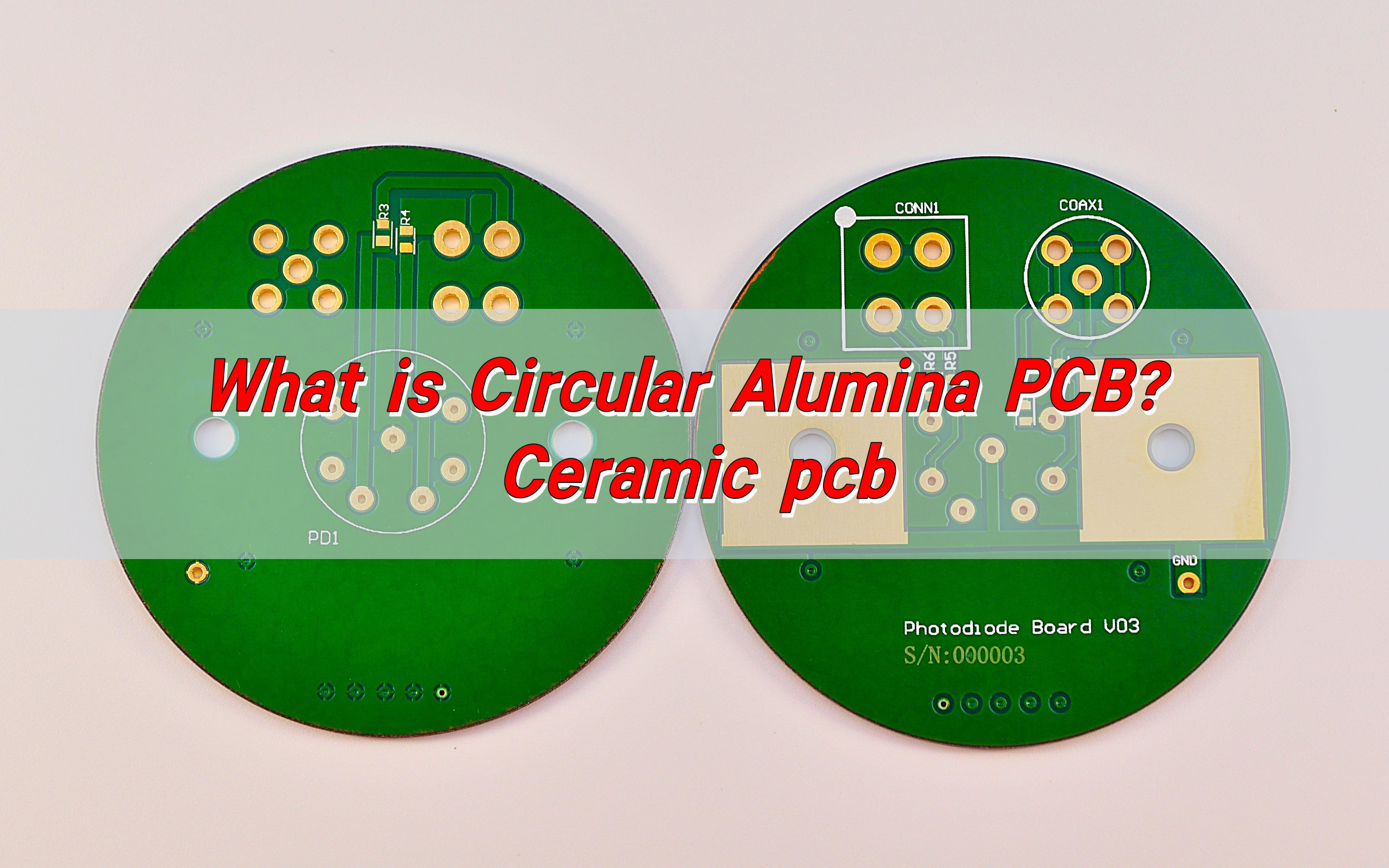
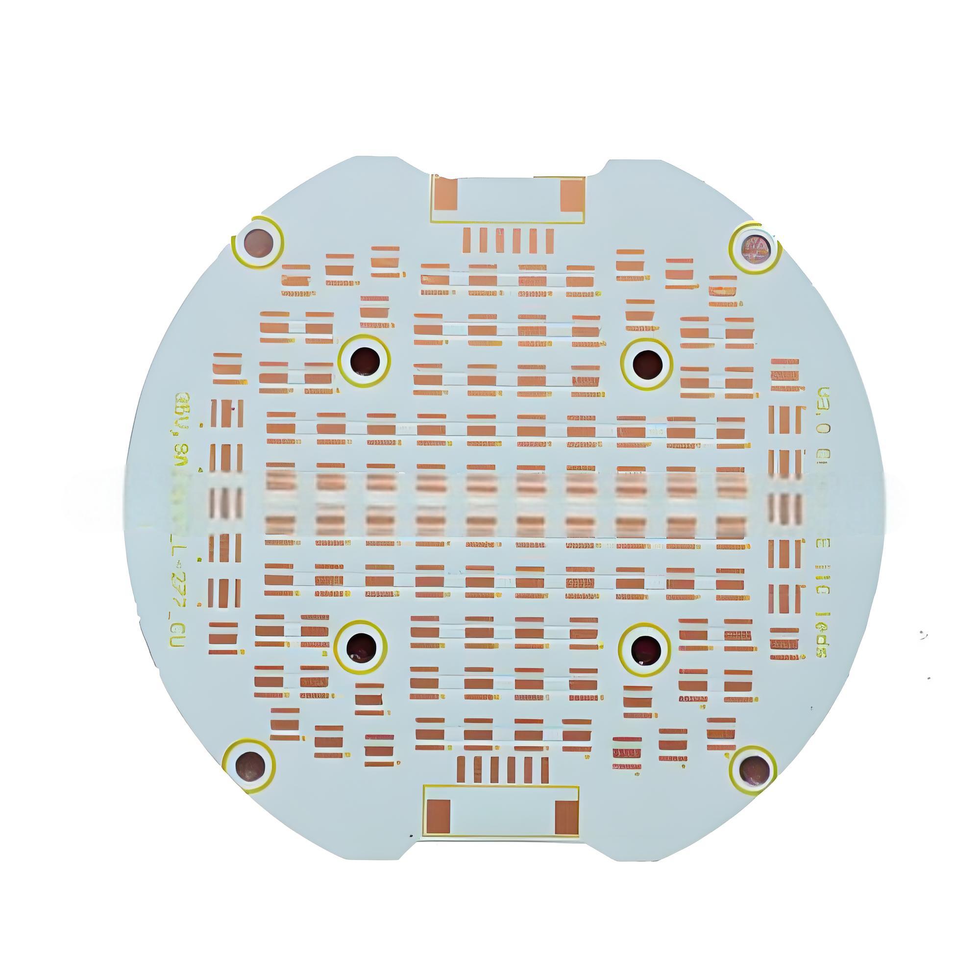
What is Circular Alumina PCB? Circular Alumina PCB is a special shape of printed circuit board, whose substrate material is alumina. Alumina PCB has excellent thermal conductivity and electrical insulation properties, so it is often used in electronic devices that require high heat dissipation and high insulation. The circular design allows this PCB to have greater design flexibility in space-constrained application scenarios.

What is Circular Alumina PCB? Ceramic pcb

What is Alumina PCB?

An alumina PCB is a type of ceramic PCB that is made using alumina (Al₂O₃), a form of aluminum oxide. It’s commonly used in applications where high thermal conductivity, electrical insulation, and mechanical strength are required.

Alumina has excellent electrical insulating properties, making it an ideal substrate for high-performance electronic devices. It can handle high-power applications and is used in industries like automotive, aerospace, telecommunications, and medical devices.

Alumina PCB materials are generally available in different grades, with 96% alumina being the most common, although higher purities like 99% alumina are also available for specialized applications.

What is a Ceramic PCB?

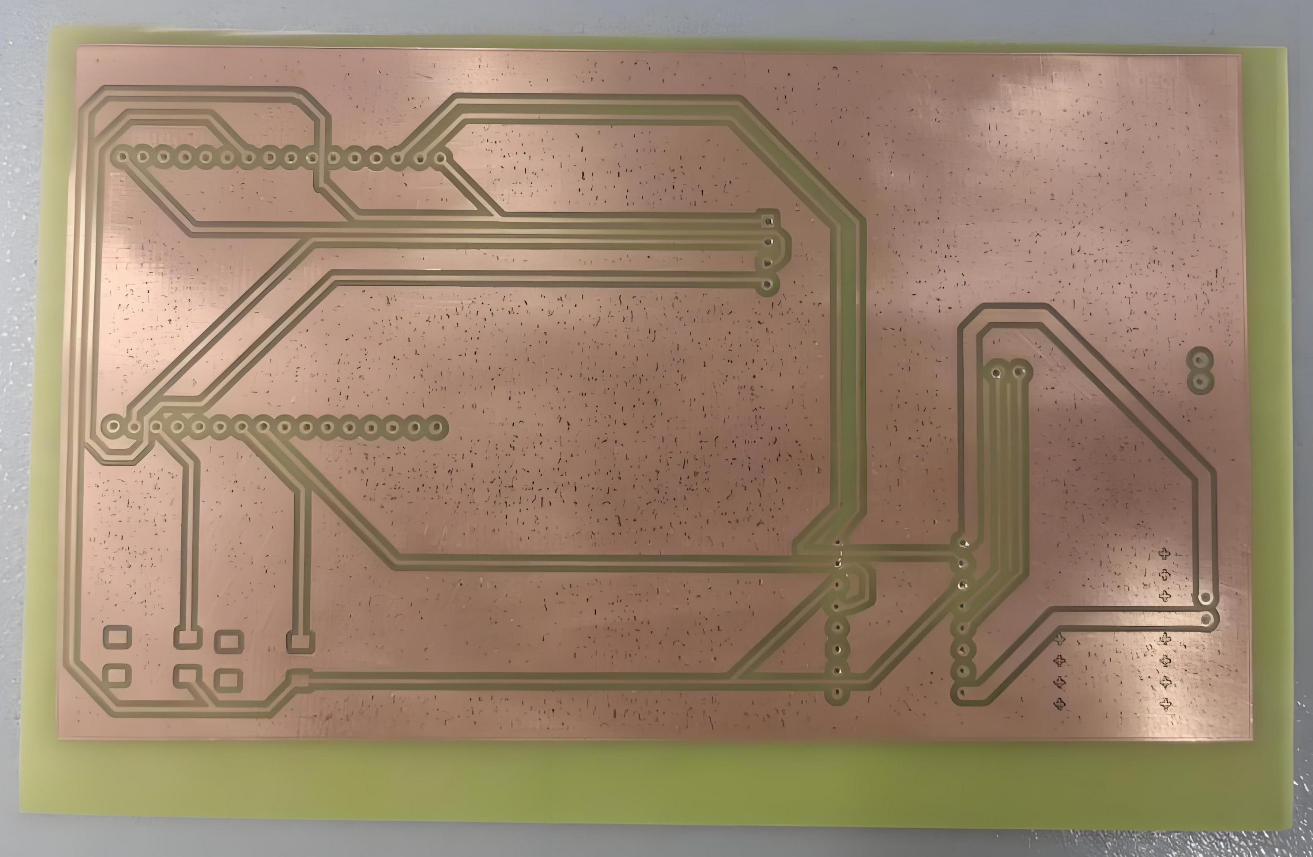
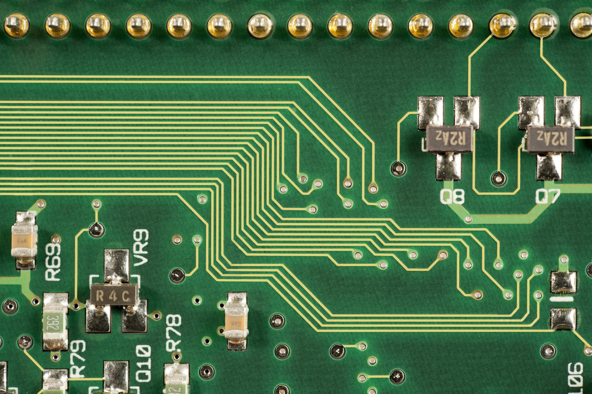
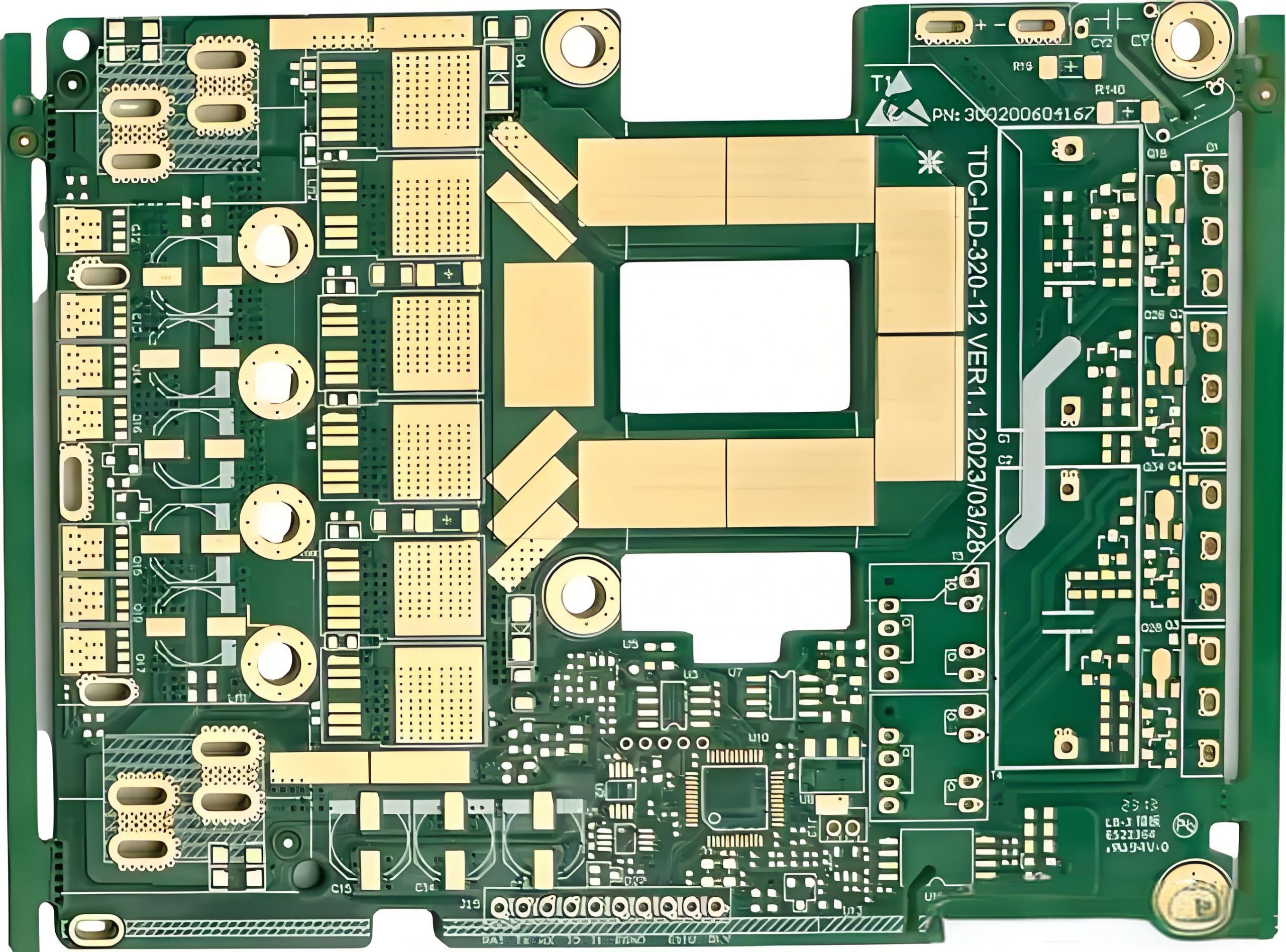
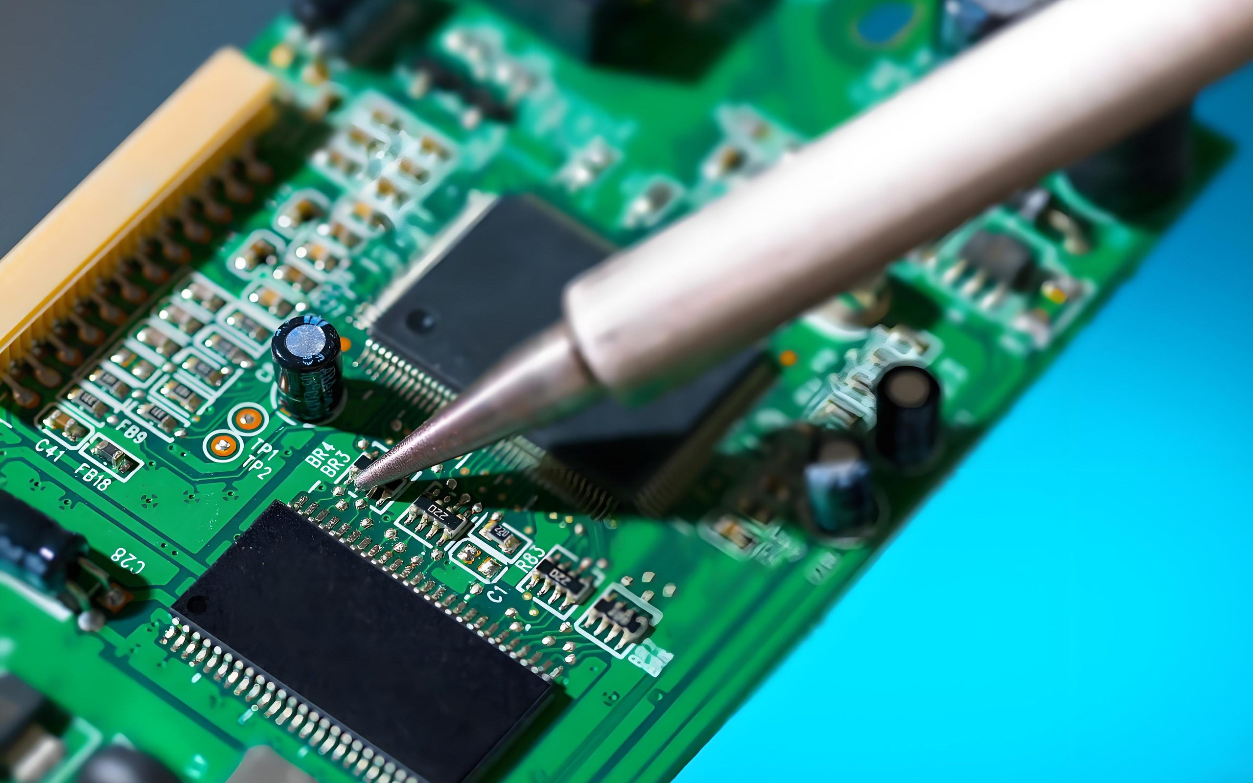
A ceramic PCB is a type of printed circuit board that uses ceramic material as a substrate. Unlike traditional FR4 PCBs, which use fiberglass-based epoxy resin, ceramic PCBs offer significantly better heat dissipation and electrical performance. This makes them an essential component in high-power and high-frequency applications.

Alumina is one of the most widely used materials for ceramic PCBs, thanks to its balanced combination of thermal and electrical properties.

What is Circular Alumina PCB? Ceramic pcb

Ceramic PCBs, including alumina PCBs, are more rigid, more durable, and better suited for environments with high temperature and stress. These PCBs can be designed with complex features, making them adaptable to a wide range of electronic products.

Is Alumina the Same as Ceramic?

Yes, alumina is a type of ceramic material, but not all ceramics are alumina. Alumina (Al2O3) is one of the most commonly used ceramic materials in PCB manufacturing due to its excellent properties, such as high thermal conductivity and electrical insulation.

Other types of ceramic materials used in PCBs include aluminum nitride (AlN), which offers even better thermal conductivity, and beryllium oxide (BeO), which is known for its high thermal conductivity and electrical properties.

So while alumina is a ceramic, the term “ceramic PCB” covers a broader range of materials.

How Thick is Alumina PCB?

The thickness of alumina PCB can vary depending on the specific needs of the application. Typically, alumina ceramic PCBs are manufactured in thicknesses ranging from 0.2 mm to several millimeters. The standard thickness for alumina substrate PCBs is about 0.5 mm to 1 mm, but it can be customized according to the requirements of the design.

The thickness of the PCB affects its ability to dissipate heat and handle electrical signals, so selecting the right thickness for your application is essential. Thicker boards offer better thermal management, while thinner boards are more suitable for compact designs where space is at a premium.

What is the Dielectric Constant of Alumina PCB?

The dielectric constant of alumina PCB typically ranges between 9 and 10, depending on the purity of the material and its specific formulation. The dielectric constant is a measure of the material’s ability to store electrical energy in an electric field, and it plays a crucial role in the performance of a PCB, especially in high-frequency applications.

A lower dielectric constant allows for faster signal transmission, which is why alumina PCB boards are often used in RF (radio frequency) and microwave circuits. However, the dielectric constant also needs to be matched to the requirements of the circuit to ensure the best performance. Alumina’s dielectric constant is ideal for most general-purpose applications, making it a versatile choice for many industries.

Is Higher Dielectric Constant Better for PCB?

Not necessarily. While a higher dielectric constant can be beneficial in certain applications, it does not always translate into better performance. The choice of dielectric constant depends on the nature of the application.

In general, higher dielectric constants are preferred in situations where energy storage is critical, such as in capacitors. However, for high-speed signal transmission, a lower dielectric constant is usually preferred, as it allows signals to travel faster with less signal loss.

Alumina’s dielectric constant strikes a good balance for most general applications, providing reliable performance across various circuit types.

What is Alumina PCB Used For?

Alumina PCBs are used in a wide range of applications where high-performance and reliability are critical. Some of the primary uses include:

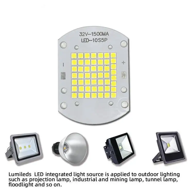
  • Power Electronics: Alumina PCBs are ideal for high-power applications, such as power supplies, LED lighting, and motor drivers, thanks to their excellent thermal conductivity.
What is Circular Alumina PCB? Ceramic pcb
  • RF and Microwave Circuits: The material’s low signal loss and high thermal conductivity make it perfect for radio frequency (RF) and microwave applications.
  • Aerospace and Defense: The aerospace industry often uses alumina ceramic PCBs due to their resistance to harsh environmental conditions, as well as their high thermal performance.
  • Automotive Electronics: Automotive applications, such as engine control units (ECUs) and power modules, benefit from the reliability and durability of alumina PCBs.
  • Medical Devices: Many medical devices require components that can operate in extreme conditions, and alumina PCBs are an excellent choice for these applications.
  • Telecommunication Equipment: The need for reliability and performance in telecom systems makes alumina a key material in the manufacturing of components like signal processors and amplifiers.

The circular alumina PCB is particularly useful in applications where the board needs to have a rounded or disk-like shape for integration into specific enclosures or devices.

What are the Disadvantages of Alumina PCB?

While alumina PCBs offer many advantages, there are some drawbacks to consider, though they are few. Some of the potential disadvantages include:

  • Brittleness: Ceramic materials like alumina can be brittle and prone to cracking or breaking under mechanical stress. Proper handling during manufacturing and assembly is required to minimize the risk of damage.
  • Cost: Alumina PCB boards are generally more expensive than traditional FR4 boards, mainly due to the cost of raw materials and the specialized manufacturing process. However, for high-performance applications, the benefits far outweigh the costs.
What is Circular Alumina PCB? Ceramic pcb
  • Manufacturing Complexity: The production of alumina ceramic PCBs is more complex compared to other types of PCBs, requiring specialized equipment and processes, which may add to the lead time.
  • Limited Design Flexibility: Although alumina PCBs are highly customizable, they are not as versatile in terms of form factors and design as some other PCB materials, like FR4. Designing highly intricate, fine-pitch circuits on alumina can be more challenging.

Despite these limitations, alumina remains a highly popular choice for a wide variety of high-performance applications, particularly where durability, heat dissipation, and electrical insulation are key requirements.

Conclusion:

The circular alumina PCB is a highly effective and versatile option in the world of high-performance electronics. Its combination of excellent thermal conductivity, electrical insulation, and mechanical strength makes it ideal for demanding applications in fields like telecommunications, aerospace, automotive, and medical devices.

BEST Technology specializes in manufacturing circular alumina PCBs with excellent manufacturing capabilities. Circular alumina PCBs are made of high-purity alumina materials, which have excellent thermal conductivity, mechanical strength and electrical insulation. They are widely used in LED lighting, automotive power control modules and other fields. If you have any needs, please feel free to contact us at sales@bestpcbs.com.

You may also like

What is 0.4mm thickness PCB? Ultrathin PCB
Thursday, January 9th, 2025

What is 0.4mm thickness PCB? 0.4mm thickness PCB is an ultra-thin printed circuit board with a thickness of only 0.4 mm. This type of PCB has high requirements in design and manufacturing, because its thinness makes it easy to cause problems such as warping and deformation during processing. 0.4mm thickness PCB is usually used in electronic devices with strict requirements on space and weight. It can meet the development trend of miniaturization and thinness of modern electronic products.

What is 0.4mm thickness PCB? Ultrathin PCB

What is a 0.4mm Thickness PCB?

A 0.4mm thickness PCB refers to a printed circuit board with a thickness of 0.4 mm. ‌This thickness of PCB is generally considered to be the minimum thickness starting point for multi-layer PCB design, suitable for application scenarios that require highly integrated and compact design‌.

0.4mm PCB has the following characteristics:

  • Thin design‌: Suitable for electronic products that require highly integrated and compact design, such as smartphones, tablets and other portable devices.
  • High reliability: Due to its thin design, 0.4mm PCB performs well in complex wiring and fine design, and can provide stable electrical performance and mechanical strength.
  • ‌Cost-effectiveness‌: Although the manufacturing process is more complicated, the overall cost is relatively low because it uses less material.

0.4mm PCB is mainly used in the following fields:

  • Portable devices: Such as smartphones, tablets, wearable devices, etc., which require lightweight and powerful circuit boards.
  • High-density interconnect applications: In occasions where high integration and complex wiring are required, 0.4mm PCB provides a better solution.
  • Radio frequency identification (RFID) and smart cards: Such as RFID tags, IC cards, SIM cards, etc., these applications require circuit boards that are both thin and reliable.

What are the advantages of 0.4mm thickness PCB?

0.4mm thickness PCB has the following advantages:

  • Reduced material cost: Due to the use of less expensive materials such as copper, the material cost of 0.4mm thickness PCB is lower.
  • Compatibility with advanced technologies: PCBs of this thickness are compatible with advanced technologies such as laser direct imaging and can be used without damaging flexible circuits.
What is 0.4mm thickness PCB? Ultrathin PCB
  • High reliability: Ultra-thin PCBs can host custom repeatable routing paths, reduce rework, and have higher reliability.
  • Strong protection: The conductors on these PCBs have a polyimide cover layer to protect against a range of potentially harsh conditions, such as vibration and acceleration on the joints.
  • High durability: 0.4mm thick PCBs can withstand millions of bending cycles and are suitable for applications that require frequent bending.

In addition, 0.4mm thick PCBs are suitable for a variety of application scenarios, including RFID smart cards, IC cards, SIM cards, electronic tags, mobile phone charging modules, wearable devices, etc.

What are the disadvantages of 0.4mm thickness PCB?

The disadvantages of 0.4mm thickness PCB mainly include the following aspects:

  • Difficulty in manufacturing: Due to the thinness of 0.4mm thickness PCBs, they are easily affected by external factors during the manufacturing process, which increases the difficulty and cost of manufacturing.
  • Lower mechanical strength: Thinner PCBs are more likely to deform or be damaged when subjected to external forces, especially in environments with high-frequency vibration or mechanical shock, which may affect their stability and reliability.
  • Poor heat dissipation: Thinner PCBs have a relatively small heat dissipation area, which is not conducive to the rapid dissipation of heat, and may cause local overtemperature, affecting the stable operation of electronic components.
  • Increased welding difficulty: During the welding process, thinner PCBs are easily affected by the welding temperature, which may cause loose welding points or welding defects.
  • Signal transmission problems: Thinner PCBs may affect the integrity and transmission speed of signals due to the shorter signal path when transmitting high-frequency signals.

How to make 0.4mm thickness PCB?

There are many aspects to consider when making 0.4mm thickness PCBs.

1. Material selection

  • Substrate: Select a substrate suitable for 0.4mm thickness. Generally, 0.3mm raw materials are used to make 0.4mm PCB boards. The type of substrate is usually FR-4 or other materials suitable for thin boards.
  • Copper foil thickness: The thickness of the copper foil affects the conductivity and strength of the PCB. Common copper foil thicknesses include 1 ounce (about 35 microns), 2 ounces (about 70 microns), etc.

2. Production process

  • Cutting: Cutting large-sized copper foil boards into small pieces suitable for production.
  • Drilling: Drilling is the first process for the formal production of circuit boards, including electrical holes, mechanical holes, vias, etc. For 0.4mm thick PCBs, laser drilling may be required to achieve smaller apertures.
  • Lamination: By combining different core thicknesses and prepreg sheets, a finished PCB thickness of 0.4mm can be achieved.
  • Electroplated: Electroplated after drilling to ensure good conductivity in the hole.
  • Solder mask: Add a solder mask to the surface of the PCB to protect the copper wire from oxidation and prevent short circuits during welding.
  • Surface treatment: Common surface treatment methods include immersion gold, tin spraying, etc. to improve the conductivity and oxidation resistance of the PCB.

What are the difficulties in making a 0.4mm thick PCB?

The main difficulties in making a 0.4mm thick PCB include the following aspects:

  • Lamination difficulties: As the copper thickness increases, the line gap is deeper, and more resin filling is required, which increases the complexity and cost of processing.
  • Drilling difficulties: As the board thickness increases, the drilling difficulty increases. Thick copper boards are usually thicker than 2.0mm, and new knives and segmented drilling techniques are required to reduce the difficulty when drilling.
  • Thermal management: Due to the increase in power consumption of electronic devices, thermal management has become a key challenge. When designing, it is necessary to consider appropriate heat dissipation structures and heat dissipation component layouts to ensure that components work properly and avoid thermal damage.
  • ‌Signal integrity‌: High-frequency signals and high-speed digital signal transmission need to consider issues such as signal loss, impedance matching, and interlayer crosstalk.
  • ‌Electromagnetic compatibility (EMC) and electromagnetic interference (EMI): Measures need to be taken to reduce electromagnetic radiation and improve anti-interference capabilities.
  • Process and material selection: Choose the appropriate printing method and substrate material to ensure that the circuit board that meets the requirements is manufactured.

How to deal with the warping problem of 0.4mm thick PCB?

There are several ways to deal with the warping problem of 0.4mm thick PCB:

  • Choose high Tg board: Boards with higher Tg can withstand higher temperatures and reduce warping caused by temperature changes. Although the cost is higher, it can effectively resist high temperature deformation.
  • Reduce via restrictions: The via design in multilayer boards should be reasonable to avoid excessive restrictions on the cold expansion and contraction of the board and reduce warping.
  • Control temperature changes: Appropriately reduce the reflow temperature or slow down the heating and cooling speed to reduce the expansion and contraction of materials caused by temperature changes.
  • Use laser drilling technology: Laser drilling can reduce stress during processing and reduce the risk of warping.
  • Mechanical leveling: Use a flattening machine to mechanically level the PCB, which is suitable for PCBs with moderate warping.

The following aspects can be used to deal with the warping problem of 0.4mm thickness PCB:

What should I pay attention to when using 0.4mm thickness PCB?

The following points should be noted when using 0.4mm thickness PCB:

  • Trace spacing and width: On 0.4mm thickness PCB, the trace spacing is usually recommended to be no less than 0.2mm to ensure stable signal transmission and reduce interference. The trace width should be designed according to the current carried. Usually the width of the power line should be between 1.2~2.5mm, and the width of the signal line should be between 0.2~0.3mm.
  • Wiring rules: In high-density and high-precision PCB design, the line width and spacing are generally set to 0.3mm. If solder mask defined (SMD) pads are used, the thickness of the traces between the pads should be appropriately reduced to avoid the problem of pad lifting during soldering or desoldering.
What is 0.4mm thickness PCB? Ultrathin PCB
  • Heat dissipation and mechanical support: For devices with high power consumption, 0.4mm thick PCBs may not be enough to provide sufficient mechanical support and heat dissipation performance. For such devices, it is recommended to choose a thicker PCB to provide better mechanical support and heat dissipation performance.
  • Design details: When designing the PCB, it should be noted that the spacing between components should be greater than 0.5mm, and the spacing between the chip pins and peripheral devices should be greater than 1.0mm. In addition, the width of the ground line should be greater than the power line to ensure a stable current supply.

0.4mm thick PCB has become an ideal choice for modern electronic products such as smartphones and wearable devices due to its ultra-thin characteristics, meeting the development needs of miniaturization and thinness. However, problems such as warping are prone to occur during production. As a professional PCB manufacturer, BEST Technology has strong manufacturing strength to ensure that each 0.4mm thick PCB effectively reduces the occurrence of warping. If you have corresponding needs, please feel free to contact us at sales@bestpcbs.com!

You may also like

What are COB led boards? COB LED Strip
Wednesday, January 8th, 2025

What are COB led boards? COB led boards are an LED light source that uses Chip On Board technology. It directly encapsulates multiple LED chips on the same substrate and then connects them to the circuit board through a special connection technology. Compared with traditional LED light sources, COB led boards share a heat dissipation substrate for multiple LED chips, which can dissipate heat more effectively and improve heat dissipation efficiency.

What are COB led boards? COB LED Strip

What are COB led boards?

COB led boards, full name Chip On Board, is a high-power LED light source that directly encapsulates multiple LED chips on an aluminum substrate.

COB led boards connect multiple LED chips in parallel, place them side by side on the same substrate, and emit and focus light by sharing the same optical lens.

COB led boards are mainly used in fields with high requirements for light efficiency and brightness, such as outdoor lighting, automotive lighting, backlighting, etc. In addition, COB led boards are also used in ultra-high-definition display solutions, especially in small micro-pitch LED display screens, which can effectively improve viewing experience and safety.

How to design COB led boards?

Designing COB (Chip On Board) led boards requires the following key steps and technical points to be considered:

1. Substrate selection

  • Material selection: Substrates are usually made of materials with high thermal conductivity and high reflectivity. Metal substrates are relatively low in cost, while ceramic substrates have better heat dissipation performance.

2. Packaging

  • Coating protective layer: Apply a layer of organic glue or resin on the LED chip and leads to protect the chip and solder joints and prevent damage to them from the external environment.
  • Lens design: According to application requirements, lenses can be added to the surface of the led boards to optimize light distribution and improve lighting effects.

3. Heat dissipation design

  • Heat dissipation structure: The heat dissipation of COB led boards mainly depends on the substrate, so the heat dissipation performance of the substrate is very important. Auxiliary heat dissipation measures such as heat sinks and heat pipes can also be used to further improve the heat dissipation efficiency.
  • Chip arrangement: Reasonably design the chip arrangement spacing to avoid heat accumulation caused by too dense chips.

4. Optical design

  • Color temperature and color rendering index: Select the appropriate color temperature and color rendering index according to the application scenario.
  • Mixed light design: For COB LED boards with multiple primary colors, it is necessary to reasonably design the arrangement and driving mode of LED chips of different colors to achieve a good mixed light effect.

5. Circuit design

  • Drive circuit: Design a suitable drive circuit to ensure the stable operation and good electrical performance of the LED chip.
  • Intelligent control: For application scenarios that require intelligent control, an intelligent dimming system can be integrated to adjust the lighting brightness according to actual usage.

How to make COB led boards?

The production of COB led boards can be summarized into the following steps:

1. Prepare the substrate

Select the appropriate substrate material and clean it to ensure the smooth progress of the subsequent process.

2. Glue dispensing and mounting

Apply an appropriate amount of conductive glue on the LED chip placement point on the substrate to achieve electrical connection between the chip and the substrate.

What are COB led boards? COB LED Strip

Place the LED chip accurately on the glue dispensing position. You can use a vacuum suction pen or tweezers to operate it, and then put the substrate with the chip attached into a thermal cycle oven and keep it at a constant temperature for a period of time. Take it out after the conductive glue is cured.

3. Wire welding

Use an aluminum wire welding machine to electrically connect the LED chip to the electrode on the substrate to form an inner lead welding to ensure a good electrical connection between the chip and the substrate.

4. Glue dispensing and curing

Prepare fluorescent glue according to the required color temperature, and then use an automatic glue dispensing machine to cover the fluorescent glue on the chip resistor and LED chip on the substrate.

Put the substrate with fluorescent glue applied in the oven for baking to completely cure the fluorescent glue to achieve the required color temperature and light effect.

5. Detection and packaging

Inspect the soldered substrate, repair or replace the LED chips that do not emit light, and repair or replace the chip resistors that do not work properly to ensure the performance and quality of the led boards.

Apply a layer of organic glue or resin on the LED chips and leads to protect the chips and solder joints and prevent them from being damaged by the external environment.

How do COB led boards work?

The working principle of COB led boards is mainly based on its packaging structure and electrical connection method:

  • Electrical connection: COB led boards are composed of multiple LED chips, which are directly adhered to the substrate through conductive glue. The substrate is usually made of metal or ceramic with good electrical and thermal conductivity.
  • Light-emitting process: When the power supply is connected to the COB led boards, the current flows through each LED chip through the circuit on the substrate, making the chip emit light. The light emitted by each chip is reflected and scattered by the packaging material to form a uniform light field.
  • Heat dissipation mechanism: A significant advantage of COB led boards is its excellent heat dissipation performance. Since the LED chip is directly attached to the substrate, the heat can be quickly conducted to the external environment through the substrate, which effectively reduces the temperature of the chip and prolongs its service life.

What is the lifespan of a COB led?

The lifespan of a COB led board is usually between 50,000 and 100,000 hours. This lifespan range means that under normal working conditions, COB led boards can last for many years. The long lifespan of COB led boards is mainly due to its good heat dissipation performance and compact packaging structure.

What are COB led boards? COB LED Strip

What are the advantages of COB led boards?

COB led boards have the following advantages:

1. Optical performance

  • High brightness and uniformity: COB led boards can provide higher brightness output by integrating multiple LED chips. Its light emission is uniform and soft, without ghosting and light spots, and can achieve a more uniform light field.
  • Wide viewing angle: COB packaging adopts shallow well spherical light emission, which has a better optical diffuse color effect.
  • High color rendering: COB light source has a high color rendering index and good color rendering, which can provide more natural and accurate light.

2. Heat dissipation performance

  • Excellent heat dissipation capacity: Multiple LED chips of COB led boards share a heat dissipation substrate, which quickly conducts heat to the external environment through the substrate, thereby effectively reducing the chip temperature and extending the service life.

3. Cost-effectiveness

  • Low cost: Compared with traditional SMD packaging, COB light source modules can save device packaging costs in lighting applications.
  • High manufacturing efficiency: The COB packaging process is simplified, eliminating the process of patch and reflow soldering, and the production efficiency is higher.

4. Structure and application

  • Light and thin: COB led boards have a simple structure and can use PCB boards of different thicknesses according to customer needs, reducing the weight to about 1/3 of traditional products, which is convenient for transportation and installation.
  • Anti-collision and pressure resistance: COB packaging encapsulates the LED chip in the concave lamp position of the PCB board, and then encapsulates and cures it with epoxy resin glue. The surface of the lamp point is convex into a spherical surface, which is smooth and hard, resistant to collision and wear.
  • Bendable: COB packaging has the ability to bend, and the bending of the PCB will not damage the packaged LED chip, so various special-shaped screens can be easily made.
  • Easy to maintain: COB light source has a simple structure and is easy to maintain. You only need to clean the optical lens to maintain brightness.

What are the disadvantages of COB led boards?

Although COB led boards have many advantages, they also have some disadvantages:

  • Heat dissipation problem: Due to the dense arrangement of chips, the heat dissipation area is limited, which easily leads to heat accumulation, affecting the light efficiency and life.
  • Relatively low light efficiency: Part of the light is absorbed after reflection between chips, resulting in a light efficiency that is about 10% lower than that of SMD packaging.
What are COB led boards? COB LED Strip
  • Difficult to repair: The chip and substrate are packaged as one, and a single chip needs to be replaced if it is damaged, and the repair cost is high.
  • High initial cost: High requirements for materials and processes, resulting in relatively high initial costs and prices.
  • Limited color selection: Mainly monochrome, the color selection is not as rich as SMD LED.

In summary, as an innovative chip-on-board packaging technology, COB led boards, with its unique principle, have shown significant advantages in light uniformity, heat dissipation, reliability and other aspects, and are widely used in indoor and outdoor lighting and display fields. BEST Technology has advanced COB packaging technology, efficient heat dissipation design, strict quality management system and flexible customization services. Please feel free to communicate with us at sales@bestpcbs.com for the production of COB led boards.

You may also like

How to copy PCB board? PCB reverse engineering
Wednesday, January 8th, 2025

How to copy PCB board? PCB reverse engineering. First, get the PCB sample to be copied, then disassemble and record the component information on the sample to make a BOM table; then scan the sample to get its PCB layout image; then trace the routing and place the components according to the image to complete the drawing of the PCB diagram; finally, use the drawn PCB diagram to make a new PCB board, solder the corresponding components, and test and debug to ensure normal function.

How to copy PCB board? PCB reverse engineering

What is copy PCB?

PCB copying, also known as circuit board cloning, refers to the reverse analysis of the circuit board through reverse research and development technology on the premise of existing electronic products and circuit boards, restoring the original product’s PCB files, bill of materials (BOM), schematic files and other technical files, and using these technical files to make PCB boards, solder components, test and debug, and finally complete the complete copy of the original circuit board sample.

How to copy PCB?

The process of copying PCB can be divided into the following points:

1. Get the PCB board to be copied and scan and back it up, remove the components and record the information to make a BOM table, and clean the residue on the surface of the PCB board.

2. Scan the cleaned PCB board, import it into the copy board software, draw the routing and place the components according to the image, and export the PCB file.

3. Make the PCB file into a PCB board, test and debug after soldering the components, and ensure that the copied PCB board functions normally.

What are the steps to copy PCB?

The process of copying PCB can be divided into the following steps:

1. Preparation

  • Get the PCB board: First, you need a PCB board, which can be provided by the customer or available on the market.
  • Scan and back up: Scan and back up the PCB board for reference during the copying process.

2. Remove components

  • Remove components: Use tools such as hot air guns to remove components on the PCB board, pay attention to temperature control, and avoid damaging components or PCB.
  • Make a BOM table: Record the model, parameters, location and other information of the removed components, and make a bill of materials.

3. Clean the PCB board

  • Remove residues: Clean the tin slag and other residues on the surface of the PCB board after the components are removed.

4. Copy board

  • Scan the PCB board: Scan the cleaned PCB board again to obtain a clear image.
  • Import the copy board software: Import the scanned image into the copy board software.
  • Draw the routing and place components: In the copy board software, draw the routing of the PCB according to the scanned image and place the corresponding components.
  • Export PCB file: Export the drawn PCB design to PCB file format.
How to copy PCB board? PCB reverse engineering

5. Make and test

  • Make PCB board: Make the exported PCB file into a PCB board.
  • Weld components: Weld the purchased components to the made PCB board.
  • Test and debug: Test and debug the welded PCB board to ensure its normal function.

Notes:

  • Legal compliance: When copying PCB, you need to pay attention to relevant laws and regulations to avoid infringement of intellectual property rights.
  • Precision control: During the scanning, drawing and production process, the precision must be strictly controlled to ensure that the copied PCB board is consistent with the original board

Does copy PCB comply with regulations?

Whether the copy PCB complies with regulations depends mainly on the purpose of the copy and whether the relevant intellectual property laws are complied with.

  • Intellectual property respect: The intellectual property rights of the original design must be respected when copying the PCB.
  • Legality of reverse engineering: In some cases, copying PCBs through reverse engineering is allowed, but the premise is that such behavior must be used for legitimate purposes.

In summary, whether the copying of PCBs is legal depends mainly on the purpose of the copying and whether the corresponding intellectual property license has been obtained. If it is for commercial purposes and without permission, it may violate relevant laws and regulations and face legal risks.

What are the benefits of copying PCB?

The benefits of copying PCBs mainly include the following aspects:

  • Save time and cost: By copying PCBs, companies can avoid the high cost and time cost of designing from scratch. Especially in urgent and complex projects, it can significantly save time and manpower.
  • ‌ Improve R&D efficiency: Copying PCBs can accelerate the product R&D process, shorten the product R&D cycle, and enable products to be brought to market faster.
How to copy PCB board? PCB reverse engineering
  • Optimize performance and function: Copying PCB is not just a simple copy. Through the analysis and research of technical data, product performance and function can be optimized, thereby enhancing the market competitiveness of products.
  • Avoid intellectual property issues: By copying PCB, enterprises can avoid infringing on the intellectual property rights of others under the premise of legality.

What should I pay attention to when copying PCB?

The following points should be noted when copying PCB:

  • Back up the original file: Before starting to copy, be sure to back up the original PCB file and GERBER file.
  • Strict file operation: During the copying process, the PCB board must be remade strictly in accordance with the content in the GERBER file, and it cannot be modified at will.
  • Check the file content: After exporting the GERBER file, you need to carefully check the file content to ensure the accuracy of the copy board content.
  • ‌Processing inner layer circuits: When processing the inner layer circuits, since there are only copper foil and inner circuits, the actual circuits cannot be seen, and the inner layer circuits need to be checked through the outer layer circuits.
  • Copper plating: When plating copper, the copper foil and the inner circuit connection need to be disconnected to avoid connection with the outer circuit.
  • Proofread with CAM software: After the design is completed, use CAM software for proofreading to ensure the accuracy of the copy board content.
  • Record component information: Before copying, record the model, parameters and position of all components in detail, especially the direction of diodes and transistors and the direction of IC gaps.
  • Disassemble and clean the PCB board: Remove all components, clean the PCB board, clean it with alcohol, dry it, and put it in the scanner.
  • Image processing: Adjust the contrast and brightness to make the parts with and without copper film have a strong contrast. Remove noise, scratches, etc.
  • Generate PCB file: Convert the processed image to PROTEL format file, import it in PROTEL and compare whether the PAD and VIA positions are accurately overlapped.
  • Merge and verify: Import TOP.PCB and BOT.PCB in PROTEL and merge them into a complete PCB diagram. Use a laser printer to print the TOP layer and BOTTOM layer on a transparent film at a 1:1 ratio, and compare it with the original PCB to ensure that there is no error.

How does BEST Technology copy PCB?

As a professional PCB manufacturer, BEST Technology has the following process for copying PCB:

1. Submit sample photos

  • Customer operation: Please take clear photos of the PCB samples, including the component layout and routing details on both sides, and then send the photos to our email: sales@bestpcbs.com
  • Notes: Make sure the photos are clear enough to clearly show the component model, location and routing on the PCB board so that our engineers can conduct preliminary analysis and evaluation.
How to copy PCB board? PCB reverse engineering

2. Preliminary quotation and communication

  • Engineer evaluation: After receiving the sample photos, our engineers will give a rough copy price based on factors such as the complexity of the PCB in the photos, the number and type of components, etc.
  • Program and IC information: If the PCB contains a program IC, you need to inform us or provide a clear photo of the IC so that we can evaluate the difficulty and cost of program cracking and give a more accurate quotation.

3. Confirm the price and send samples

  • Price confirmation: After receiving our preliminary quotation, if you have any questions or need to adjust, you can communicate with us further until both parties reach an agreement on the price.
  • Sample delivery: After the price is determined, you need to send us PCB samples, preferably 2 samples, so that we can conduct more detailed analysis and cloning. After receiving the samples, we will provide you with an accurate quotation based on the actual sample situation.

4. Payment and production start

  • Payment process: After you confirm that the final quotation is correct, you will complete the payment according to our payment method.
  • Production start: After receiving the customer’s payment, we will officially start the PCB cloning work, including sample analysis, component disassembly, PCB drawing and other steps.

5. Provide design files and manufacture circuit boards

  • Design file delivery: After completing the copy board work, we will send you the complete Gerber file, schematic diagram and BOM (Bill of Materials) for your review and confirmation.
  • Circuit board manufacturing: After confirming that the design files are correct, we will start to manufacture circuit boards for you based on these files to ensure that the quality and performance of the circuit boards meet your requirements.

In summary, every step of the PCB copy process is meticulous to ensure that the copy board accurately restores the original board function. At the same time, it is very necessary to find a qualified PCB manufacturer. BEST Technology has rich experience in PCB manufacturing. If you have PCB copy needs, please feel free to contact us at sales@bestpcbs.com.

You may also like

What is remote control PCB? PCB Design & Production
Tuesday, January 7th, 2025

What is remote control PCB? The remote control PCB is an electronic circuit board inside the remote control, which is used to connect and support various electronic components to realize signal transmission and processing. It connects the microcontroller, communication module, input components, and power management components through conductive lines, so that the remote control can receive the user’s input signal, convert it into a control signal, and realize remote control of equipment such as TVs and air conditioners.

What is remote control PCB? PCB Design & Production

What is remote control PCB?

The remote control PCB refers to the printed circuit board used in the remote control. It is the core component inside the remote control, responsible for connecting various electronic components to realize various functions of the remote control.

The remote control PCB is usually composed of multiple layers of conductive metal (usually copper foil) and insulating materials. These metal layers are designed into a complex circuit network, and the combination of wiring and insulating materials enables electronic components to achieve electrical connection and functional integration.

The electronic components on the PCB include resistors, capacitors, transistors, integrated circuits (ICs), etc. They are connected together through the metal network on the PCB to form a complete circuit, thereby realizing various functions of the remote control.

The types of remote control PCB mainly include single-sided board, double-sided board and multi-layer board:

  • Single-sided board: the most basic PCB type, suitable for simple circuit design.
  • Double-sided board: wiring on both sides, suitable for more complex circuit design.
  • Multi-layer board: can be further divided into middle and bottom boards and high-layer boards, mainly used for high-end equipment.

Remote control PCB is widely used in various electronic devices. Through the design and layout of PCB, the reception, processing and output of remote control signals can be realized, so as to control the switch, volume adjustment, channel selection and other functions of related equipment.

How to design remote control PCB?

Designing remote control PCB requires comprehensive consideration of functional requirements, component selection, circuit design, layout and wiring, power management, signal integrity, electromagnetic compatibility and thermal design.

What is remote control PCB? PCB Design & Production

1. Functional requirements analysis

  • Determine the control function: clarify which devices and functions the remote control needs to control, such as switch, volume adjustment, channel switching, etc.
  • Signal transmission method: Select a suitable signal transmission method, select the corresponding components and design layout according to the signal type.

2. Component selection

  • Microcontroller (MCU): Select a suitable MCU, and select an MCU with sufficient processing power and input/output interface according to functional requirements.
  • Communication module: Select the corresponding communication module according to the signal type, such as infrared transmission module, radio frequency module or Bluetooth module.
  • Input component: Select a suitable button, touch screen or other input component for user operation and control.
  • Power management component: Select a suitable power management component, such as battery management chip, voltage regulator, etc., to ensure a stable power supply.

3. Circuit design

  • Draw a circuit schematic: Use circuit design software (such as Altium Designer, Eagle, etc.) to draw a circuit schematic and connect all components according to functional requirements.
  • Check the circuit: Carefully check the circuit schematic to ensure that all connections are correct, there are no short circuits or open circuits, etc., and perform circuit analysis and simulation to verify the feasibility of the circuit.

4. PCB layout and wiring

  • Layout: PCB layout should be carried out according to the schematic diagram, and the position of components should be arranged reasonably to minimize signal interference and noise. High-frequency components and sensitive components should be kept away from power lines and ground lines.
  • Wiring: When wiring PCB, try to use short and straight lines to avoid long lines and too many corners. Pay attention to the layout of signal lines and ground lines to ensure stable signal transmission.
  • Impedance matching: For high-frequency signal lines, impedance matching design should be carried out to reduce signal reflection and interference and improve the reliability of signal transmission.

5. Power supply design

  • Power supply circuit: Design a reasonable power supply circuit, including power input, filtering, voltage regulation and other parts to ensure stable power supply and avoid the influence of power supply noise on the circuit.
  • Power management: Design a power management strategy according to the power consumption requirements of the remote control to extend battery life.

6. Signal integrity and electromagnetic compatibility

  • Signal integrity: For high-speed and high-frequency signals, perform signal integrity analysis and design, optimize signal transmission paths, reduce signal distortion and reflection, and ensure signal integrity.
  • Electromagnetic compatibility (EMC): Take measures to improve the electromagnetic compatibility of PCB, reduce electromagnetic interference and radiation, and meet relevant EMC standards.

7. Thermal design

  • Heat dissipation design: According to the power consumption and heat dissipation requirements of the components, perform heat dissipation design, reasonably arrange heat dissipation components, and ensure that the components are within the normal operating temperature range.
  • Thermal management: Use thermal management strategies to improve the heat dissipation performance of PCB.

8. Testing and verification

  • Functional test: Perform functional test on remote control PCB to ensure that all functions work properly, including signal transmission, input response, etc.
  • Performance test: Perform performance test to ensure that the performance of PCB meets the design requirements.
  • Reliability test: Perform reliability test, such as vibration test, temperature cycle test, etc., to ensure the reliability and stability of PCB in various environments.

What does the remote control PCB consist of?

The main components of remote control PCB include mainboard, remote control chip, battery interface, button, indicator light and shell. Among them, the motherboard is the core part of the entire circuit board, and the remote control chip is an important part of controlling the remote control.

  • Motherboard: The core part of the circuit board, carrying other electronic components.
  • Remote control chip: Process key signals, encoding signals and control other circuit components.
  • Battery interface: Provide power support for other components on the circuit board.
  • Key module: Receive user operation instructions and convert the instructions into electrical signals.
  • Indicator light: Display the status or function of the remote control.
  • Shell: Protect internal components and provide users with a grip.

How does a remote control PCB work?

The working principle of the remote control PCB mainly involves signal generation, transmission and reception.

1. User input

  • Button or touch screen operation: The user selects the function or command to be controlled by pressing a button or touching the screen. These input devices convert the user’s operation into electrical signals and send them to the microcontroller (MCU).
What is remote control PCB? PCB Design & Production

2. Signal processing

  • Microcontroller processing: After receiving the input signal, the microcontroller processes and encodes the signal according to the preset program logic.
  • Coding: Control signals are usually encoded into a specific format for easy transmission and identification. The encoded signal contains complete information required for device control.

3. Signal transmission

  • Infrared transmission: For infrared remote control, MCU sends the encoded signal to the infrared transmitting module, which converts the electrical signal into an infrared light signal and transmits it through the infrared transmitting diode.
  • RF transmission: For RF remote control, MCU sends the encoded signal to the RF module, which modulates the signal to a specific frequency and transmits it. RF signals have stronger penetration and longer transmission distance.
  • Bluetooth transmission: For Bluetooth remote control, MCU transmits the signal to the receiving device wirelessly through the Bluetooth module, which is responsible for signal modulation, encoding and transmission.

4. Signal reception

  • Receiving device: The receiving device (such as TV, air conditioner, etc.) is equipped with a corresponding receiving module to receive the signal sent by the remote control.
  • Decoding and execution: After receiving the signal, the receiving module decodes it, converts it into a control instruction, and then performs the corresponding operation according to the instruction.

Through the above steps, the remote control PCB realizes the complete process from user input to device control, enabling users to conveniently operate various devices remotely.

How to produce remote control PCB?

The production process of remote control PCB mainly includes the following steps:

  • Design stage: The design stage includes determining the function of the circuit, laying out components, drawing wire paths, etc.
  • Raw material preparation: According to the design requirements, purchase suitable substrate materials, such as FR-4, which has good insulation, mechanical strength and cost-effectiveness, and is suitable for most common electronic products.
  • Cutting and drilling: Cut the copper clad board into the required size, and use a high-precision drilling machine to drill precise through holes on the circuit board. These holes will be used for electrical connections between different layers.
  • Copper deposition: The hole wall of the PCB is bulked to enhance adhesion, and then a copper foil layer is deposited on the hole wall by electrochemical method to ensure the conductivity of the hole.
  • Line exposure: Use LDI technology to accurately project the circuit diagram onto the copper clad layer of the PCB, and form the prototype of the circuit diagram through exposure and development of the photosensitive dry film.
  • Electroplating: Further increase the thickness of the copper layer on the developed circuit and hole wall to ensure its conductivity and mechanical strength.
  • Outer layer etching: Etch the outer layer of the PCB to form the required circuits and pads.
  • Gold treatment: Perform gold treatment on the exposed key PAD position to protect the copper layer and prevent oxidation.
  • Shape treatment: Perform shape treatment on the PCB substrate and finally complete the production.

What should we pay attention to during the production of remote control PCB?

In the production process of remote control PCB, the following key aspects need to be paid attention to to ensure product quality and performance:

1. Design stage

  • Design review: Ensure that the circuit design is correct and meets the functional and manufacturing requirements.
  • Follow standards: Strictly follow industry standards and specifications, such as IPC standards, to ensure the manufacturability of the design.

2. Material selection

  • High-quality materials: Select substrate materials and copper foil that meet the specifications to ensure good insulation and conductivity.
  • Supplier management: Select suppliers with good reputation to ensure stable and reliable material quality.

3. Manufacturing process

  • Process control: Strictly control key process parameters such as exposure, etching, and lamination to ensure the stability and consistency of the production process.
  • Standard Standardized operation: formulate detailed operating procedures to ensure that operators operate according to unified standards and reduce human errors.

4. Quality inspection

  • Intermediate inspection: set up multiple inspection points during the production process to find and correct problems in time.
  • Finished product inspection: conduct comprehensive finished product inspection, including functional testing, electrical performance testing and appearance inspection, to ensure that the product meets quality standards.
  • Thermal management: rationally layout heat dissipation components and heat dissipation channels to ensure that the components are within the normal operating temperature range.
  • Electromagnetic compatibility: take measures to improve the electromagnetic compatibility of PCB and reduce electromagnetic interference and radiation.

Through the above measures, the production quality of remote control PCB can be effectively improved to ensure its reliability and performance in practical applications.

How to choose a suitable remote control PCB supplier?

Selecting a remote control PCB supplier can be considered from the following points:

1. Comprehensive strength

  • Production capacity: pay attention to the production line, equipment and workers to ensure that the production scale and delivery period can be met, and understand the ability to respond to emergency orders.
  • Technical level: check whether there are advanced process capabilities and R&D teams, and whether they can provide technical support.
  • Quality control: examine whether there are quality certifications and complete testing processes and equipment.
What is remote control PCB? PCB Design & Production

2. Service quality

  • Pre-sales service: see whether it can provide comprehensive technical consultation, respond to needs in a timely manner, and provide quotations and samples.
  • After-sales service: understand the after-sales guarantee policy and team situation.

3. Reputation

  • Customer evaluation: view other customer evaluations through various channels.
  • Industry status: understand its popularity and cooperation in the industry.

4. Price cost

  • Price comparison: compare multiple quotations, pay attention to price composition and long-term cooperation discounts.
  • Cost-effectiveness evaluation: comprehensively consider quality, service, etc. to evaluate cost-effectiveness.

As a professional PCB manufacturer, BEST Technology has strong design and technical support capabilities, and can provide customized remote control PCB design solutions according to customer needs, and ensure reasonable layout and stable signals.

At the same time, we have advanced production equipment and flexible production scale, which can efficiently produce various types of remote control PCBs to meet the needs from small batch proofing to large batch production; in terms of quality control, we follow a strict quality management system and use advanced testing equipment for comprehensive testing to ensure that the quality of each PCB is reliable and defect-free.

In addition, we focus on on-time delivery, provide high-quality customer service and technical support, and respond quickly to customer needs to ensure that customers are worry-free during use and enjoy a good service experience.

You may also like

What Do You Know About FFC Cables, Flexible Flat Cables?
Tuesday, January 7th, 2025

FFC cables refer to flexible flat cables, which are typically flat and can bend in multiple directions, making them ideal for compact, portable devices such as smartphones, laptops, and other electronics.

The unique design of FFC cables allows them to save space while ensuring a stable electrical signal transmission. These cables are often used when traditional, bulkier cables wouldn’t fit or could compromise the device’s design or functionality.

What Are FFC Cables?

FFC cables, or Flexible Flat Cables, are a type of electrical cable designed to transmit power and signals in a compact and flexible manner. These cables are made up of flat, thin conductors that are arranged in a specific pattern. What makes them stand out is their flexibility, allowing them to be bent, twisted, and routed through tight spaces without compromising their functionality. FFC cables are typically used in applications where space is limited but high performance is essential.

Their compact size and flexibility make FFC cables ideal for devices like mobile phones, laptops, cameras, and printers, where flexibility and space optimization are key. The design of FFC cables ensures they can be easily routed around corners or into confined spaces, making them invaluable in modern electronics.

What Are the Different Types of Flat Flex Cables?

Flat Flex Cables (FFC) are generally classified into two main types based on the alignment of their conductive contact points:

1. Type A (Same-Side Contact): The conductive contacts on both ends of the cable are on the same side. Commonly used when the connectors or devices at both ends have contacts facing the same direction. Ideal for straightforward and simple wiring setups.

2. Type B (Reverse-Side Contact): The conductive contacts on the two ends of the cable are on opposite sides. Typically used when connectors or devices at both ends require contacts on opposing sides.

What Does the Pitch of FFC Cables Refer to?

The pitch of FFC cables refers to the distance between the centers of two adjacent conductive strips (or contacts) on the cable. It is measured in millimeters (mm) and is a critical specification for ensuring compatibility with connectors or devices.

The pitch indicates how closely the conductive strips are spaced. Common pitch sizes for FFC cables include 0.5mm, 1.0mm, 1.25mm, and 2.54mm, among others.

The pitch must match the spacing of the pins in the connector. Mismatched pitches can lead to poor connections or damage to the cable or device.

Smaller pitches (e.g., 0.5mm) are often used in compact electronic devices like smartphones and laptops. Larger pitches (e.g., 2.54mm) are preferred for applications requiring higher current or mechanical durability.

What Is the Size of Flexible Flat Cable?

The size of a flexible flat cable (FFC) can vary widely, depending on its application and design. In terms of width, FFC cables are typically available in sizes ranging from 1.0 mm to 1.5 mm. However, the size can be customized to meet the specific requirements of the application. The thickness of these cables is usually quite thin, with typical FFC cables measuring only a few millimeters thick. This compact size allows them to fit into tight spaces and be routed easily in small devices.

As for the number of conductors, FFC cables can come with anywhere from a few to several dozen conductors, depending on the complexity of the signal or power they need to carry. This makes them highly adaptable to a wide variety of uses, from simple connections to complex multi-wire systems.

What Is the Maximum Length of FFC Cables?

The maximum length of FFC cables depends on several factors, including the type of cable and the power or signal it carries. Generally, FFC cables are available in lengths ranging from a few millimeters up to several meters. However, the longer the cable, the more important it becomes to consider factors like signal integrity, resistance, and the quality of the materials used.

In most cases, FFC cables are designed for short to medium distances, typically within the range of 50 cm to 2 meters. However, for specialized applications, custom lengths can be manufactured. It’s important to note that longer cables may require additional shielding or signal conditioning to maintain signal quality over the distance.

What Is the Difference Between FFC and FPC Cables?

While both FFC and FPC cables share similar characteristics, there are key differences that set them apart:

Design: FFC cables are made up of flat conductors that are spaced apart, whereas FPC cables have conductors printed directly onto a flexible substrate. This means that FPC cables can offer more complex circuit designs.

Application: FFC cables are generally used for more straightforward applications that require flexibility and simplicity, such as in consumer electronics. On the other hand, FPC cables are often used in highly specialized applications, including medical devices and aerospace, due to their ability to support more complex layouts.

Flexibility: While both types are flexible, FPC cables are often more flexible than FFC cables due to their thinner and more precise construction. This gives FPC Cables an advantage in applications that require frequent bending or folding. Best Technology offers a wide range of FPC products with high quality, tailored to meet the specific needs of each customer. Reach out to us at sales@bestfpc.com for more details.

Cost: FFC cables are usually less expensive to produce, while FPC cables, with their intricate designs and specialized applications, can be costlier.

Choosing between FFC and FPC cables depends largely on the complexity and requirements of the application. Both offer distinct advantages depending on your needs.

How to Choose FFC Cables?

Choosing the right FFC cables requires understanding the specific needs of your project. Here are some key factors to consider when selecting FFC cables:

Width and Pitch: Determine the width and pitch of the cable to ensure it fits in the space and connectors you are working with. Common pitch sizes are 0.5 mm, 1.0 mm, and 1.25 mm.

Conductor Count: Consider how many conductors you need for your application. More conductors are necessary for complex circuits or multiple connections.

Shielding: If your application is sensitive to electromagnetic interference (EMI), choose a shielded FFC cable to protect your signal integrity.

Length: Consider how far the signal needs to travel. Shorter cables are usually more efficient, but longer cables can be customized as needed.

Environment: If the cable will be exposed to extreme temperatures or harsh conditions, make sure to select a cable with the appropriate protective coatings or materials.

By evaluating these factors, you can ensure you choose the right FFC cables for your application.

What Are FFC Cables Used For?

FFC cables are used in a wide variety of applications where space is limited and flexibility is required. Some of the most common uses include:

Consumer Electronics: In devices like smartphones, laptops, tablets, and cameras, FFC cables connect internal components while maintaining a small profile.

Automotive Applications: FFC cables are used to connect sensors, controls, and displays in vehicles, providing both flexibility and reliability.

Medical Devices: These cables are often used in diagnostic equipment, portable devices, and other medical technologies where compact and flexible wiring is essential.

Industrial Equipment: FFC cables play a key role in controlling robotics, automation, and other industrial equipment that requires flexible connections.

Consumer Appliances: They are also used in household appliances like printers, washing machines, and microwaves for internal wiring connections.

The versatility of FFC cables makes them an ideal solution for numerous industries that require reliable, flexible, and space-saving connectivity.

What Are the Benefits of Flexible Flat Cable?

Flexible flat cables provide a number of key advantages that make them ideal for modern applications:

Space Efficiency: Due to their flat and thin design, FFC cables are perfect for applications where space is limited. They can be routed through tight spaces, making them ideal for compact devices.

Flexibility: These cables can be bent and twisted, allowing them to be routed around corners or other obstacles without damaging the conductors. This flexibility is particularly useful in dynamic environments where cables need to move.

Ease of Use: FFC cables are easy to install and require minimal space for connections. Their flat design allows for quick connections in a variety of environments.

Signal Integrity: Shielded FFC cables can provide excellent protection against electromagnetic interference, ensuring that your signals remain clear and strong.

Customization: FFC cables can be tailored to meet the specific needs of your application, with various pitches, lengths, and conductor counts available.

Overall, the benefits of flexible flat cables make them an excellent choice for many modern electronic and industrial applications, offering a balance of performance, flexibility, and compact design.

By focusing on the advantages and versatility of FFC cables, this blog provides readers with a comprehensive understanding of their types, uses, and benefits while maintaining a clear, approachable, and professional tone.

You may also like

How thick is 2 oz of copper on a PCB?
Friday, January 3rd, 2025

How thick is 2 oz of copper on a PCB? The thickness of 2 oz of copper on a PCB is about 70μm. Ounces are the common unit of PCB copper foil thickness. The thickness of 1 oz copper foil is generally about 35μm, so the thickness of 2 oz copper foil is about twice that of 1 oz, which is about 70μm.

How thick is the copper on a PCB board?

The copper layer thickness on a PCB board is usually between 1oz (35μm) and 4oz (140μm), while the copper layer thickness of a thick copper board can exceed this range, even reaching 10oz or more.

How thick is 2 oz of copper on a PCB?

Copper layer thickness selection in different application scenarios

  • Signal transmission: For signal transmission, a copper layer thickness of 1oz is usually sufficient, because signal transmission mainly focuses on signal integrity and stability.
  • High current applications: For applications that need to withstand high currents, such as power supplies and industrial control equipment, 2oz or higher copper layer thicknesses are more suitable because they provide better conductivity and carrying capacity.
  • Special applications: In some special applications, such as motor controllers and battery management systems for new energy vehicles, the high performance of thick copper boards can meet their stringent requirements.

What is the standard thickness of the copper layer on a PCB?

The standard thickness of the copper layer on a PCB usually ranges from 1oz to 4oz. The specific choice depends on the application scenario and requirements. For signal transmission, a thickness of 1oz is usually sufficient; for occasions that require high current, 2oz or 3oz copper thickness is more suitable.

Application scenarios of copper layers of different thicknesses

  • 1oz copper thickness: suitable for general signal transmission, such as ordinary double-sided boards.
  • 2oz copper thickness: suitable for occasions that require larger currents, such as power boards.
  • 3oz copper thickness: suitable for high current and high power applications, such as some special industrial equipment.

The choice of copper layer thickness is mainly based on the purpose of the circuit board, the signal voltage and the current. In addition, thicker copper layers can improve the electrical performance and load-bearing capacity of the circuit board, but it will also increase the manufacturing cost.

How to calculate PCB thickness?

The calculation of PCB thickness mainly depends on the thickness of the copper foil and the number of layers and structure of the PCB.

The thickness of the copper foil is usually expressed in ounces (OZ), and 1OZ copper foil is approximately equal to 35 microns (um) or 1.4 mils (mil). Common PCB copper foil thicknesses are 17.5um, 35um, 70um, etc.

How thick is 2 oz of copper on a PCB?

The thickness of the multilayer board also needs to consider the lamination loss, which is usually related to the residual copper rate of the inner copper foil. The specific formula for calculating the lamination thickness is: Lamination thickness = PP theoretical thickness – lamination loss.

What is the difference between 1oz and 2oz copper PCB?

The main difference between 1oz and 2oz copper PCBs is the thickness of the copper foil and the applicable scenarios.

1. Copper foil thickness:

  • 1oz copper thickness: 1oz copper thickness means that the weight of copper foil per square foot of board area is 1 ounce (about 35.3 grams), and the corresponding copper foil thickness is about 1.4 mils (0.035mm).
  • 2oz copper thickness: 2oz copper thickness means that the weight of copper foil per square foot of board area is 2 ounces (about 70.6 grams), and the corresponding copper foil thickness is about 2.8 mils (0.071mm).

2. Applicable scenarios:

  • 1oz copper thickness: Suitable for most common circuit board designs and applications because it is low cost and can meet general needs.
  • 2oz copper thickness: Suitable for applications that require higher current carrying capacity, such as power electronic devices and high-power LEDs.

3. Cost:

  • 1oz copper thickness: It is a common choice due to its low cost.
  • 2oz copper thickness: Due to the thicker copper foil, the cost is relatively high.

How thick is the copper in a flex PCB?

The copper thickness in a flexible PCB is usually 1/3 ounce (OZ), 1/2OZ, 1OZ and 2OZ, and the corresponding physical thickness is 12μm, 18μm, 35μm and 70μm respectively.

How thick is 2 oz of copper on a PCB?

Choosing the right copper thickness is a key link in the design of flexible boards, and factors such as the application requirements, cost and technical feasibility of the circuit board need to be considered. Thicker copper foil can provide better current conduction, reduce resistance and heat generation, and improve the stability and efficiency of the circuit, but at the same time it will increase the cost and processing difficulty.

What is the thickness tolerance of copper in PCB?

The thickness tolerance standard of copper in PCB mainly depends on the type and specification of the board used.

According to the GB/T 4722 standard, the common PCB board copper thickness standard tolerances are as follows:

  • 0.5mm board thickness: coarse tolerance is ±0.07mm, fine tolerance is ±0.01mm.
  • 0.7mm board thickness: coarse tolerance is ±0.15mm, fine tolerance is ±0.09mm.
  • 0.8mm plate thickness: rough tolerance is ±0.15mm, fine tolerance is ±0.09mm.
  • 1.0mm plate thickness: rough tolerance is ±0.17mm, fine tolerance is ±0.11mm.
  • 1.2mm plate thickness: rough tolerance is ±0.18mm, fine tolerance is ±0.12mm.
  • 1.5mm plate thickness: rough tolerance is ±0.20mm, fine tolerance is ±0.14mm.
  • 1.6mm plate thickness: rough tolerance is ±0.20mm, fine tolerance is ±0.14mm.
  • 2.0mm plate thickness: rough tolerance is ±0.23mm, fine tolerance is ±0.15mm.
  • 2.4mm plate thickness: rough tolerance is ±0.25mm, fine tolerance is ±0.18mm.
  • 3.2mm board thickness: the rough tolerance is ±0.30mm, and the fine tolerance is ±0.20mm.

In addition, according to the IPC-6011 standard, the inner layer copper thickness tolerance is usually 10%, and the outer layer copper thickness tolerance is usually +20%. For PCBs with a thickness of less than 1mm, the board thickness tolerance is ±10% of the board thickness; for PCBs with a thickness greater than or equal to 1mm, the board thickness tolerance is ±0.10%.

How to choose PCB copper layer thickness?

There are several key factors to consider when choosing the thickness of the PCB copper layer:

  • Current carrying capacity: Generally speaking, the thicker the copper, the better the electrical performance of the circuit board, and it can carry more current. For power lines or high-power applications that require large currents to pass through, using thicker copper foil can effectively reduce the temperature rise of the line and avoid performance degradation or safety issues caused by overheating.
How thick is 2 oz of copper on a PCB?
  • Signal transmission quality: Thicker copper foil can reduce wire resistance, reduce attenuation and delay during signal transmission, and thus improve signal integrity. Especially in high-frequency circuit design, precise control of copper foil thickness is the key to achieving good impedance matching, reducing signal reflection and crosstalk.
  • Cost considerations: The thicker the copper, the higher the cost of the circuit board. Because thicker copper foil will increase material costs and processing difficulty, leading to an increase in overall costs.

Application scenarios Ordinary double-sided boards usually use 1oz copper thickness, while the inner layer of multi-layer boards is generally 1/2oz or 1/3oz, and the outer layer is 1oz or 1/2oz1. For circuits that require high current, 2oz or 3oz copper thickness may be used.

In short, the PCB copper thickness varies greatly. 0.5 ounce copper foil is low in cost and easy to process, suitable for simple and small products; 1 ounce is highly versatile and suitable for general electronic products; 2 ounces of copper is about 70μm thick, can carry more current, and has relatively good heat dissipation performance, but it is costly and difficult to process, and is often used in industrial equipment with extremely high power requirements. The copper thickness should be selected according to the actual situation of product function, cost, etc. to ensure that it is easy to use and economical.

You may also like

How to clean a pcb? How to clean circuit board corrosion?
Thursday, January 2nd, 2025

How to clean a pcb?First, prepare a soft brush, high-concentration isopropyl alcohol or special cleaning agent, and tweezers, and take power-off and anti-static measures. Then use a soft brush dipped in cleaning agent to brush, soak the stains in the cleaning agent first and then brush, use a cotton swab to clean the gaps and blow them clean again. After cleaning, use a low-temperature hot air blower to blow dry from a distance, and finally check whether the appearance is damaged and perform functional tests.

How do you clean up PCBs?

PCB is a key component of electronic equipment. Cleaning PCB helps ensure its normal operation and extend its service life. Here are some common cleaning methods and precautions:

How to clean a pcb? How to clean circuit board corrosion?

1. Eraser cleaning method:

  • Tools: Choose a soft eraser.
  • Operation: Gently press the eraser on the part that needs to be cleaned, such as the gold finger, and wipe back and forth along its arrangement direction until the surface is restored to brightness. This method is simple and effective, and will not damage the gold-plated layer on the surface of the gold finger.

2. Alcohol wiping method:

  • Tools: medical alcohol (or anhydrous ethanol), soft cloth or cotton wool.
  • Operation: Pour an appropriate amount of alcohol on a soft cloth or cotton wool, and then gently wipe the surface of the PCB to ensure that the alcohol is evenly covered. After wiping, wait for the alcohol to evaporate naturally.

3. Special detergent method:

  • Tools: Goldfinger special detergent, board washing water, hydrogen peroxide, etc., as well as cleaning cloth, cotton swabs or soft brushes.
  • Operation: Dilute the detergent to an appropriate concentration according to the instructions for use, then dip the detergent with a soft cloth, cotton swab or soft brush, and gently wipe the surface of the PCB. After wiping, rinse thoroughly with clean water, then wipe dry with a clean cloth or dry naturally.

4. Ultrasonic cleaning method:

  • Equipment: Ultrasonic cleaning machine.
  • Operation: First calculate and configure the dilution ratio of the cleaning solution, add water to the cleaning machine tank, and then add the cleaning solution. Preheat the solution to the appropriate temperature according to the detergent recommendation. Then put in the PCB and set the cleaning time, usually a few minutes. After cleaning, remove the PCB, rinse and dry thoroughly.

5. High-pressure spray cleaning and brushing:

  • Equipment: High-pressure spray cleaning machine or soft brush.
  • Operation: High-pressure spray cleaning is to spray the cleaning liquid onto the PCB surface at a high pressure through a high-pressure pump, and use the impact of the water flow to wash away the contaminants. Brushing is to use a soft brush to dip the cleaning liquid and manually or automatically brush the PCB surface.
How to clean a pcb? How to clean circuit board corrosion?

When cleaning the PCB, you should choose the appropriate cleaning method and tools according to the actual situation, and pay attention to the safety and effectiveness during the operation. At the same time, the cleanliness of the PCB should be carefully checked after cleaning to ensure that there are no residues and stains that affect the performance and stability of the circuit board.

Can you use WD-40 to clean a circuit board?

You can use WD-40 to clean the circuit board, but you need to be careful. WD-40 can effectively remove oil, dust, oxides and some minor corrosion on the circuit board, and can form a thin protective film on the surface of the circuit board to prevent the circuit board from getting wet.

In addition, WD-40 precision electrical cleaner is suitable for various electronic instrument circuit boards. It has the characteristics of fast cleaning and no residue. It is suitable for plastic, rubber and metal materials, safe and non-corrosive.

Advantages and disadvantages of using WD-40 to clean circuit boards

Advantages:

  • Good cleaning effect: WD-40 can effectively remove various dirt on circuit boards, especially dirt in narrow gaps and between components.
  • Moisture-proof effect: Form a protective film on the surface of the circuit board to prevent moisture, suitable for circuit boards in humid environments or long-term storage.
  • Quick drying and no residue: WD-40 precision electrical cleaner evaporates quickly without leaving any residue.

Disadvantages:

  • Need to dry thoroughly: After cleaning, you must ensure that the circuit board is completely dry, otherwise it may cause problems such as short circuits.
  • Avoid sensitive components: Avoid WD-40 directly spraying on sensitive components during cleaning, such as high-precision sensors, chip pins, etc.

What is the best solvent to clean PCB?

The best solvent for cleaning PCBs depends on the specific cleaning needs and environmental requirements.

Common solvents and their advantages and disadvantages

  • Organic solvents: such as acetone, ethanol or isopropyl alcohol. These solvents have strong dissolving power and can effectively remove dirt and grease on the surface of PCB. The advantages are simple operation, easy to obtain solvents, and suitable for most conventional cleaning needs.
  • Chlorinated solvents: For example, the washing water made by mixing chlorinated solvents with other solvents can dissolve rosin and remove flux quickly, and is easy to volatilize after cleaning, but it is often easy to turn white and sticky, and it is a flammable solvent. Environmental regulations are becoming increasingly stringent, and its use has been reduced.
  • Hydrocarbon solvents: composed of two elements, carbon and hydrogen, are mainly used to clean various oils, greases, and soldering resins. Hydrocarbon cleaning agents can be used in various ways, but they are flammable and explosive, so safety should be paid attention to when using them.
  • Water-based washing water: With water as the solute carrier, it is environmentally friendly, safe, non-toxic, and has no irritating gas volatilization. It is suitable for SMT steel mesh, fixtures, wave soldering equipment, etc., with good cleaning effect and environmental protection.

What is a good substitute for PCB cleaner?

Substitutes for PCB cleaners include alcohol, detergent, white vinegar and lemon juice. These alternatives perform well in cleaning electronic components and have less impact on the human body and the environment.

  • Alcohol: Alcohol is a relatively environmentally friendly cleaning agent that can effectively remove oil and dirt from the surface of PCBs and electronic components. Alcohol is not only affordable and easily available, but also evaporates quickly and does not leave water stains after use.
  • Dishwashing liquid: Dishwashing liquid does not contain any harmful substances and is harmless to the human body and the environment. It is also suitable for cleaning oil and dirt on the surface of PCB boards and electronic components, and is inexpensive.
  • White vinegar: White vinegar is an environmentally friendly and non-toxic natural cleaning agent that can effectively remove stains and sediments from the surface of electronic components. White vinegar is readily available in the home and is easy to use.
  • Lemon juice: Lemon juice contains acidic ingredients that can remove stains and sediments from the surface of electronic components. It is a natural cleaning agent that is non-toxic, environmentally friendly and has a natural aroma.

What breaks down PCBs?

When cleaning PCBs, the following situations may cause them to break down:

  • Chemical corrosion: Using a cleaning agent containing highly corrosive substances (such as concentrated acids, strong alkalis, and halogenated solvents) will react with the PCB substrate material and destroy its structure; the moisture or chemical components in the cleaning agent residue may also cause oxidation corrosion of the metal circuit, accelerating the aging and decomposition of the PCB.
How to clean a pcb? How to clean circuit board corrosion?
  • Physical damage: Brushes with hard bristles, sharp tools, or excessive force can scratch the circuit, damage the protective layer, or even cut the circuit, and may also cause components to loosen and fall off; high temperatures during drying can soften and deform the substrate material, affecting the quality of the solder joints and further damaging the PCB.
  • Electrostatic discharge: If anti-static measures are not taken during cleaning, static electricity will accumulate and then discharge, which may damage static-sensitive components, cause damage to the internal circuit structure, affect the PCB function, and even cause further damage such as short circuits.

Is 70% isopropyl alcohol safe for electronics?

70% isopropyl alcohol is generally safe for electronic products. It has good cleaning properties, can dissolve common stains such as oil, and has moderate volatility, which means it can evaporate quickly after cleaning. But there are risks. The 30% water it contains may harm components that are sensitive to humidity, causing short circuits, corrosion, or performance degradation.

Of course, as long as you operate carefully, avoid liquid from entering the components, and ensure complete drying, it is generally safe, but higher purity isopropyl alcohol or special cleaning agents may be required for precision or humidity-sensitive electronic products.

How to clean circuit board corrosion?

There are several ways to clean circuit board corrosion:

  • Use compressed air: Compressed air is a common tool for electronic cleaning. It can remove dust and impurities by releasing short pulses into the vents.
  • Use baking soda: Baking soda (sodium bicarbonate) is an alkaline substance that can effectively neutralize the acid in the corrosive solution and help remove corrosion on the surface of the PCB.
  • Use distilled water: Distilled water has high purity and can be used to clean circuit boards, but you need to be careful to avoid using ordinary tap water because the impurities in it may aggravate corrosion.
  • Use special cleaning agents: such as board washing water, alcohol, etc. These cleaning agents can effectively remove stains and flux residues on the circuit board.
How to clean a pcb? How to clean circuit board corrosion?
  • Ultrasonic cleaning technology: Use ultrasonic vibration to improve the cleaning effect, suitable for the cleaning needs of high-end precision products.
  • Dry ice cleaning method: This is an environmentally friendly cleaning technology that removes stains by spraying dry ice particles, suitable for precision products that are sensitive to shaking.

Methods to prevent circuit board corrosion include:

  • Keep it dry: Avoid circuit boards in a humid environment for a long time. Keeping the circuit board dry is the key to preventing corrosion.
  • Clean flux residues in time: Clean flux residues in time after welding to prevent them from reacting with PCBs and causing corrosion.

In short, cleaning PCBs is an indispensable part of electronic equipment maintenance. By choosing appropriate cleaning methods and tools, pollutants on the PCB surface can be effectively removed, and the stability and service life of the equipment can be improved. At the same time, precautions and effect inspections during the cleaning process are also very important.

You may also like

Why is copper used in PCBs?
Thursday, January 2nd, 2025

Why is copper used in PCBs? Because of its strong electrical conductivity, it can ensure efficient signal transmission; excellent thermal conductivity, can quickly dissipate heat; stable chemical properties, can resist corrosion to ensure reliable circuits; good processability, meet the needs of PCB miniaturization; and good cost-effectiveness and compatibility, it is an ideal choice for PCB manufacturing.

What material is commonly used for PCBs?

The materials commonly used for PCBs include FR-4, metal substrates, ceramic substrates, polymer materials, etc. These materials have their own characteristics and are suitable for different application scenarios.

Why is copper used in PCBs?
  • 1. FR-4

FR-4 is a glass fiber reinforced plastic and is the most commonly used substrate in the PCB manufacturing process. It has excellent electrical properties, mechanical properties, thermal properties and weather resistance, and is widely used in home appliances, office electronic equipment, automotive electronics, industrial controllers and other fields.

  • 2. Metal substrate

A metal substrate is a PCB board with a metal film plated on the substrate. Commonly used metals include aluminum, copper, iron, nickel, stainless steel, etc. It has excellent heat dissipation and shock resistance, and is suitable for high-power electronic equipment, LED lighting, automotive electronics and other fields. But metal substrates are expensive and have high manufacturing costs.

  • 3. Ceramic substrates

Ceramic substrates are very hard, high-temperature-resistant and corrosion-resistant materials, usually made of high-purity alumina or silicon nitride. They are suitable for high-frequency, high-power and high-precision electronic components, and are mainly used in high-end fields such as military industry, aerospace, and medical treatment.

  • 4. Polymer materials

Polymer materials include polyimide, acrylic, polyamide and epoxy resin, which have good mechanical properties, dimensional stability and thermal stability, and are suitable for high-density, high-speed and high-precision circuit boards. They are mainly used in semiconductor production equipment, optical instruments, aerospace, military industry and other fields.

What is the core material of a PCB?

The core material of a PCB is copper clad laminate (CCL). Copper clad laminate plays a vital role in PCB manufacturing. It not only provides the functions of conductivity, insulation and support, but also directly determines the performance of PCB.

The manufacturing process of copper clad laminate includes impregnating electronic fiberglass cloth or other reinforcing materials with resin, then covering one or both sides with copper foil, and undergoing hot pressing. This material not only has the functions of conducting, insulating and supporting, but also serves as the core substrate of PCB.

In addition, other core materials of PCB include copper foil, prepreg, dry film and ink, etc. These materials together determine the quality and performance of the final product.

What is the copper plate on PCB?

The copper clad laminate (CCL) on PCB is a composite material consisting of a non-conductive substrate (such as FR4) and one or more layers of copper foil. The copper foil is usually covered on one or both sides of the substrate for conductive connection.

Why is copper used in PCBs?

Copper clad laminate plays a vital role in PCB manufacturing. It is the core material for making PCBs and has four major functions: conducting, insulating, supporting and signal transmission.

Copper clad laminate not only carries the connection between electronic components, but also ensures the normal operation of electronic equipment, and in the production of multilayer boards, it also plays the role of core board.

The manufacturing process of copper clad laminate mainly includes impregnating the reinforcing material with a resin binder, then covering the copper foil on one or both sides, and finally hot pressing. It occupies an important position in PCB manufacturing, and direct materials account for about 60% of the total cost of PCB. It has a wide range of applications and is commonly found in electronic products such as computers, computers, and mobile communications.

Why is copper used in a PCB?

The main reasons for using copper in PCBs include the following:

  • Conductive properties: Copper is an excellent conductive material that can ensure that current flows smoothly on the PCB to meet the working requirements of electronic equipment.
  • Heat dissipation: The high thermal conductivity of copper can effectively disperse heat to a larger area, reduce local hot spots, and improve overall heat dissipation efficiency.
  • Mechanical stability: Copper plating helps maintain the uniformity of lamination during PCB manufacturing and reduce deformation caused by uneven materials, thereby improving the mechanical stability of the finished product.
  • Signal integrity: Copper plating can provide a low-impedance return path, reduce signal loss and interference, especially in high-frequency digital signal transmission, and improve the stability and reliability of signal transmission.
  • Electromagnetic shielding: Large areas of ground or power copper plating can serve as a natural electromagnetic shielding layer to reduce external interference, while suppressing noise propagation within the circuit to meet EMC requirements.
  • Reduce costs: Although the cost of copper is relatively high, its excellent electrical and thermal conductivity makes the circuit design more concise, reduces the number and complexity of components, and thus reduces the overall cost to a certain extent.

What is the purpose of copper traces on a PCB?

Copper traces on a PCB have a variety of uses, mainly including conduction, heat dissipation, mechanical support and signal transmission.

  • Conductivity: Copper traces are the most important conductive material in PCBs, used to connect various components in the circuit, such as integrated circuits, resistors, capacitors, etc., to ensure smooth transmission of current.
  • Heat dissipation: Copper has good thermal conductivity. By laying copper traces near the heat source, heat can be effectively dispersed, local overheating can be prevented, and the overall heat dissipation efficiency of the PCB can be improved.
Why is copper used in PCBs?
  • Mechanical support: Copper traces play a supporting role in the PCB manufacturing process, helping to maintain the uniformity of lamination and reduce deformation, thereby improving the structural stability of the PCB.
  • Signal transmission: In high-frequency circuits, copper traces provide a complete return path for high-frequency signals, reduce signal interference, and improve the stability and reliability of signal transmission.

How thick is 1 oz copper PCB?

The thickness of 1 oz copper PCB is about 1.4 mils, or 0.035 mm.

Key information is as follows:

  • Relationship between ounces and thickness: In PCB manufacturing, the thickness of copper is usually expressed in ounces. 1 ounce of copper means that the weight of copper is 1 ounce in an area of ​​1 square foot.
  • Unit conversion: After conversion, the thickness of 1 oz copper is about 1.4 mils, and 1 mil is equal to 0.001 inches, which is further converted to millimeters, that is, 0.035 mm.

What is the difference between 1 oz and 2 oz copper?

The main difference between 1 oz and 2 oz copper is their thickness and weight.

1. Thickness difference:

  • 1 oz copper: The thickness of 1 oz copper is about 0.0356 mm or 1.35 mils.
  • 2 oz copper: The thickness of 2 oz copper is about 0.0712 mm or 2.72 mils.

2. Weight difference:

  • 1 ounce copper: 1 ounce is approximately equal to 28.35 grams (g).
  • 2 ounces copper: 2 ounces is approximately equal to 56.7 grams (g), which is twice that of 1 ounce copper.
Why is copper used in PCBs?

3. Application scenarios:

  • 1 ounce copper: Usually used for general circuit board design, suitable for most electronic devices.
  • 2 ounces copper: Suitable for applications that require higher current carrying capacity or higher reliability, such as servers, industrial control equipment, etc.

4. Cost difference:

  • Increased thickness: Generally, increased copper thickness leads to higher costs because more materials and more complex manufacturing processes are required.

On the whole, the choice of copper in PCB is inevitable. With its excellent performance, it ensures stable signal transmission, anti-interference, efficient heat dissipation, circuit stability, high current carrying and enhanced PCB mechanical strength of electronic equipment, thereby ensuring reliable operation of the equipment.

You may also like

What is pcb board assembly? PCB assembly manufacturer
Thursday, January 2nd, 2025

What is pcb board assembly? PCB board assembly is the process of installing various electronic components (such as resistors, capacitors, chips, etc.) on the PCB and achieving electrical connections through welding and other methods to build a circuit board that can achieve specific electronic functions. This process includes component preparation, PCB board pretreatment, welding and post-assembly inspection.

What is the assembly of a PCB?

What is pcb board assembly? PCB assembly manufacturer

PCB assembly is the process of installing and electrically connecting various electronic components to a printed circuit board according to design requirements. It includes component preparation (purchase inspection, classified storage), PCB preparation (inspection, cleaning), welding (plug-in welding and patch welding) and post-assembly inspection (appearance and electrical performance inspection). Its quality is crucial to the performance and reliability of electronic products and is widely used in consumer electronics, industrial control, communications, automotive electronics and other fields.

How do you assemble a PCB board?

  • Component preparation: Purchase electronic components according to design documents and check whether the component specifications, models and appearance are qualified. After that, the qualified components are classified and stored by type, packaging form, etc.
  • PCB preparation: Check the appearance of the PCB board for scratches, short circuits and other defects, and wipe it with a special cleaner or alcohol to ensure that the surface is free of oil and dust, and that the pads are flat and free of oxidation.
  • Soldering process: Insert the component pins into the corresponding holes of the PCB, use an electric soldering iron to melt the solder to fill the pins and pads to form solder joints, and pay attention to controlling the temperature and time.
  • SMT soldering: Print solder paste on the PCB pads, place the components with a SMT machine, and then heat them according to the temperature curve through a reflow oven to melt the solder paste to form solder joints.
  • Post-assembly inspection: Perform an appearance inspection to check the solder joints and component installation. Then perform an electrical performance test, use professional equipment to check whether the function is normal, and troubleshoot and repair the faults.

What is the function of PCB assembly?

The main functions of PCB assembly include the following aspects:

  • Electrical connection: The copper wire tracks on the PCB board can connect various electronic components (such as resistors, capacitors, and integrated circuits) to form a complete circuit system. This efficient connection method simplifies circuit design and improves circuit reliability.
  • Component support: PCB provides stable support for components. Through welding and other methods, components can be firmly mounted on PCB, which improves the structural integrity and portability of the equipment.
What is pcb board assembly? PCB assembly manufacturer
  • Circuit protection: The insulating material of PCB can effectively isolate electromagnetic interference and protect the circuit from the external environment (such as moisture, dust, etc.), thereby extending the service life of electronic equipment, especially in harsh industrial environments.
  • Heat dissipation function: In high-performance, high-power electronic equipment, the metal layer (such as copper foil) on the PCB can quickly absorb and disperse the heat generated when the circuit is working, preventing components from being damaged by overheating. By optimizing the design, such as increasing the thickness and layout of the copper foil, the heat dissipation efficiency can be further improved.
  • Space optimization and compact structure: The design of the PCB is not only related to the functional realization of the circuit, but also affects the production cost, production efficiency and subsequent maintenance and replacement. Optimizing the use of space makes the internal structure of electronic equipment more compact and beautiful.

What is the standard for PCB assembly?

The standardization of PCB assembly is one of the important measures to ensure product quality and reliability. The following are the main standards for PCB assembly:

  • PCB board size and positioning: The size and positioning of the PCB board should meet the design requirements to ensure accurate alignment and fixation during the assembly process.
  • Component welding quality: The quality of the welding point is the key. The welding point should be smooth, firm, and burr-free to avoid poor welding, cold welding and other undesirable phenomena.
  • Component arrangement and layout: The arrangement and layout of the components should meet the design requirements to ensure the correct spacing and position between the components to avoid mutual interference.
  • Solder point quality: The solder joint should be firm, smooth, and burr-free to ensure the normal operation of the circuit.
  • Appearance quality: The surface of the PCB board should be clean, flat, and scratch-free, and the components should be arranged neatly and beautifully.
  • Electrical performance: Ensure that the electrical performance of the PCB after assembly meets the design requirements.
  • Weather resistance: PCB assembly should have good weather resistance and be able to work stably under different environmental conditions.
  • Reliability: The durability and reliability of the components should be considered during the assembly process to ensure stability in long-term use.

In addition, the specific assembly standards may vary depending on different application scenarios and product types. During the assembly process, relevant standards and requirements should be followed to ensure the quality and stability of the assembly.

What files are needed for PCB assembly?

The following main files are needed in the PCB assembly process:

  • Gerber file: This is the most critical file in PCB production, which contains the geometric information of each layer of the circuit board, such as copper lines, pads, solder mask and silk screen layers. Gerber files are usually generated by CAD software and saved in a standard format.
  • Drill file (.drl or .xin): This file provides the location and size information of all the drill holes on the circuit board, ensuring that the drill holes are accurately aligned with the circuit pattern.
  • Bill of Materials (BOM): The BOM lists all the materials and components that make up the circuit board, including their quantity, specifications and supplier information.
  • Coordinate files: These files provide the coordinate and orientation information of each component on the circuit board, which is essential for the automated assembly process.
  • Assembly drawings: If the PCB needs to be assembled with other electronic components, it is necessary to provide assembly drawings or assembly instructions, which detail how the components are installed on the circuit board.
  • Test requirements: If the manufacturer is required to perform specific tests, such as functional tests or electrical performance tests, it is necessary to provide test requirements or test instructions files.
  • Design Rule Check File (DRC): Used to verify whether the PCB design meets the manufacturing requirements and standards, helping to find and correct potential problems during the design stage.
  • 3D Model (STEP File): Used to generate a 3D model of the circuit board to help simulate and verify during the production process.
  • Structure Drawing (DXF format): Used to make a CAD structure drawing of the circuit board to ensure accuracy during the manufacturing process.

When providing these files, make sure they are up-to-date, accurate, and match the production requirements. It is also very important to maintain communication with the manufacturer to ensure that they have a clear understanding of the design requirements and can produce as expected.

What are the materials used in PCB assembly?

PCB assembly mainly uses the following materials:

1. Electronic components

  • Passive components: including resistors (used to control current and voltage, with a variety of resistance values, powers and packaging forms), capacitors (used to store charge and filter, there are ceramic, electrolytic, tantalum capacitors and other types, with different capacities and withstand voltage values), inductors (used to store magnetic field energy, with winding and stacked inductors, and the unit of inductance is Henry).
What is pcb board assembly? PCB assembly manufacturer
  • Active components: such as integrated circuits (including various functional circuits, with DIP, SOP, BGA and other packaging forms), transistors (used for amplification and switching functions, with BJT and FET and other types, with different parameters).

2. Welding materials

  • Solder wire: The main component is tin-lead or lead-free alloy, with different diameters, lead-containing solder wire has a lower melting point, lead-free solder wire has a higher melting point, and often contains flux inside.
  • Solder paste: used for SMT welding, it is a mixture of solder powder and flux, and its viscosity and metal content affect the quality of printing and welding.
  • Flux: used to remove metal surface oxides and reduce solder surface tension, available in liquid, paste and other forms, and ingredients include organic acids, rosin, etc.

3. PCB substrate materials

  • FR-4: Commonly used epoxy glass fiber cloth laminate, with good insulation, mechanical strength and thermal stability, and different thicknesses.
  • Ceramic substrate: excellent thermal conductivity and high-frequency performance, such as aluminum nitride and alumina ceramic substrates, suitable for high-power and high-frequency devices.
  • Flexible PCB substrate: used for bendable or foldable devices, the material is soft, and polyimide is often used as an insulating layer.

4. Other auxiliary materials

  • Cleaning agent: used to clean impurities on PCB boards, including alcohol and special electronic cleaning agents.
  • Thermal conductive materials: such as thermal grease and thermal conductive tape, used for heat dissipation of high-power components.

How is a PCB board structured?

The basic structure of a PCB board includes multiple layers, each of which has its specific functions and effects.

PCB boards are mainly composed of the following layers:

  • Top Layer: This is the top layer of the PCB board, which is usually filled with electronic components such as resistors, capacitors, and chips. The top layer not only carries these components, but also is responsible for their connection and wiring to ensure that current and signals can be accurately transmitted.
  • Bottom Layer: Located at the bottom of the PCB board, it is mainly responsible for the laying of ground wires and the connection of auxiliary signal lines. The bottom layer provides a solid support for the circuit board to ensure the stability and safety of the circuit.
  • Inner Layer: Located between the top layer and the bottom layer, it is composed of multiple layers of copper foil stacked to form a complex circuit network. The inner layer is used to conduct signals and power supply, reduce signal interference, and ensure the clarity and accuracy of the signal.
  • Solder Mask Layer: This is a special layer, the main function of which is to protect the pads on the circuit board, prevent the solder from splashing into other areas during the soldering process, and ensure the soldering quality and stability of the circuit.

What is the difference between PCB and PCB assembly?

The main difference between PCB and PCBA lies in their status and function.

1. Definition and function

  • PCB: PCB is the cornerstone of electronic devices, providing physical support and electrical connection for electronic components. It consists of a conductive copper layer and an insulating layer, and is usually manufactured by methods such as chemical etching. The PCB itself does not contain any electronic components, but is just an empty circuit board.
What is pcb board assembly? PCB assembly manufacturer
  • PCBA: Printed circuit board assembly refers to the installation of electronic components on the PCB to form a complete circuit. PCBA is functional and can be directly installed in the final product for use.

2. Cost and complexity

  • PCB: Since there are no electronic components, the manufacturing process is relatively simple and the cost is low.
  • PCBA: Due to the need to install and test electronic components, the manufacturing process is more complicated and the cost is higher. PCBA is more complex and more expensive than PCB.

3. Application

  • PCB: Mainly used to manufacture PCBA, as a support and connection frame for electronic components.
  • PCBA: After assembly, PCBA is used in various electronic devices such as computers, smartphones, home appliances, etc.

In summary, PCB board assembly is an interlocking, delicate and complex process. From the careful selection of component preparation, to the pretreatment of PCB boards, and the final strict control, each step should not be underestimated. It organically integrates various electronic components with PCB boards to become PCBA.

You may also like