pcb
Home > Blog

Archive for the ‘FAQ’ Category

What is NPTH in PCB?
Wednesday, December 18th, 2024

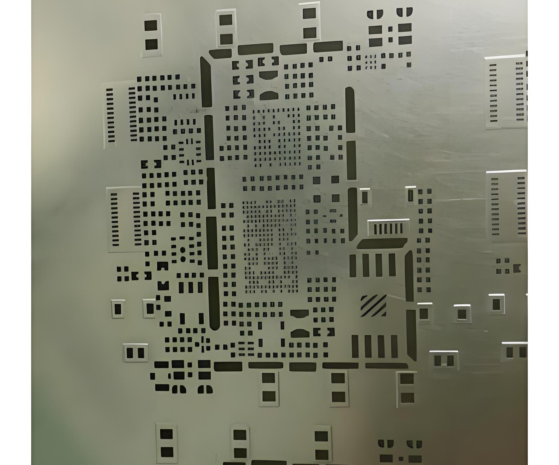
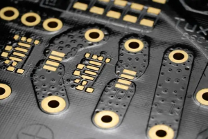
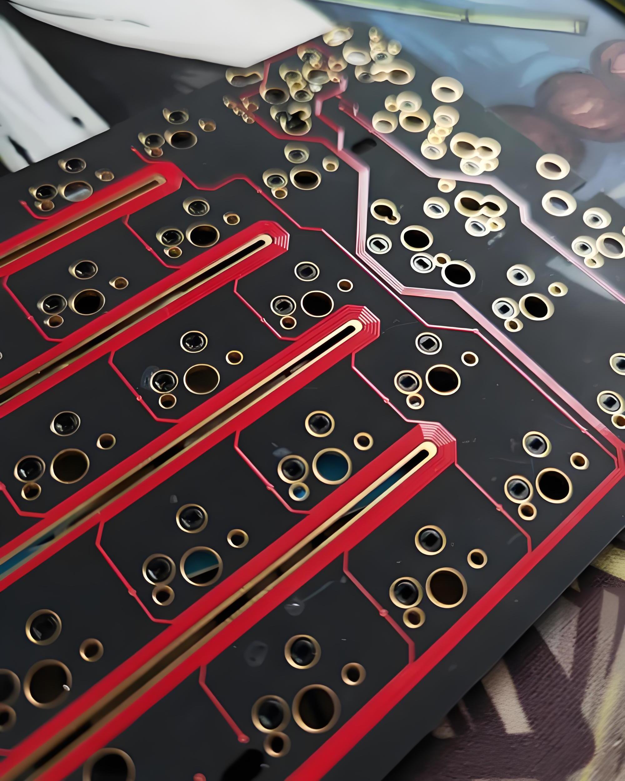
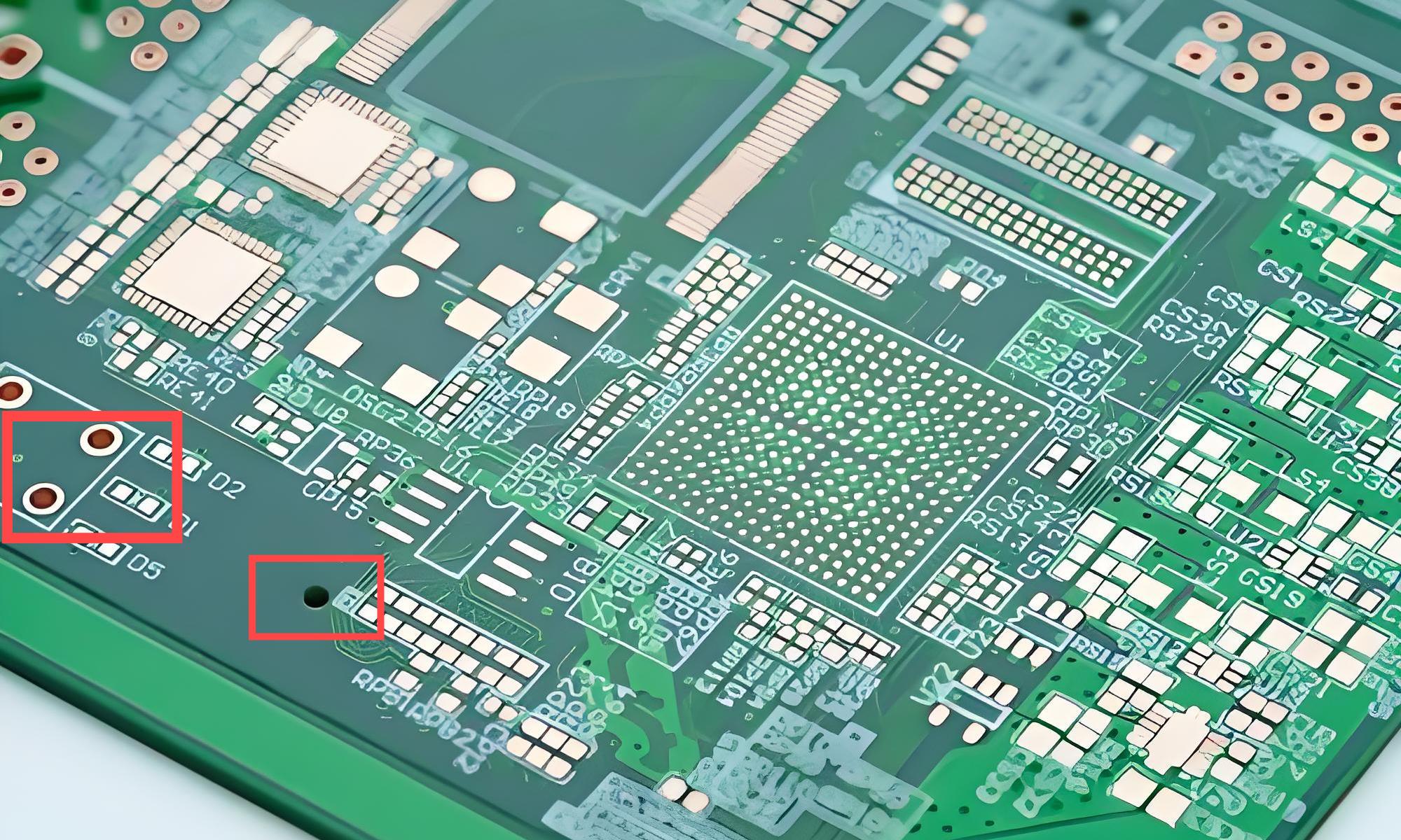
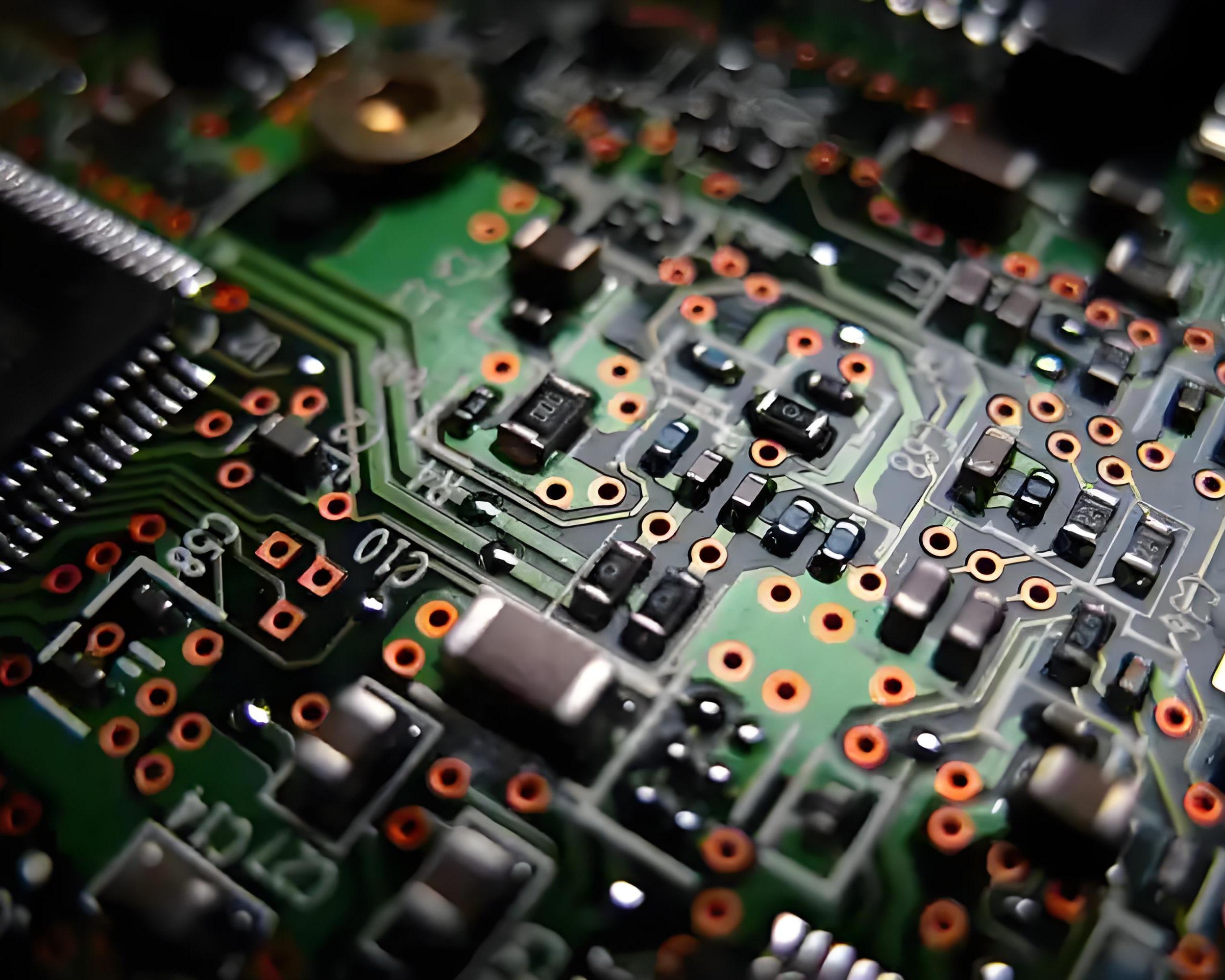
What is NPTH in PCB? NPTH is a through hole on PCB, but unlike plated through hole, its hole wall is not treated with electroplated metal. These holes are usually used for mechanical installation, positioning or as non-electrical connection purposes such as ventilation and heat dissipation channels.

What is an NPTH?

NPTH refers to non-plated through hole, that is, a hole without electroplated metal on the hole wall. The hole wall of NPTH hole is not electroplated with metal and is usually used for positioning, fixing or as a screw hole. These holes do not participate in electrical connection and are mainly used for mechanical fixing or structural support.

What is NPTH in PCB?

NPTH holes are often used in the following scenarios:

  • Positioning hole: used to position and fix other components or parts on PCB.
  • Screw hole: used to install screws and fix PCB or other components.
  • Mounting hole: used to install connectors or other external devices.

What is the full form of NPTH?

The full name of NPTH is “Non Plating Through Hole”. In printed circuit boards (PCBs), NPTH refers to holes whose walls are not plated with metal and therefore do not participate in electrical connections. Such holes are usually used for positioning, fixing screws or other non-conductive purposes.

What is the difference between PTH and non PTH?

The main difference between PTH (Plating Through Hole) and NPTH (Non Plating Through Hole) is whether the hole wall is plated.

1. Plating:

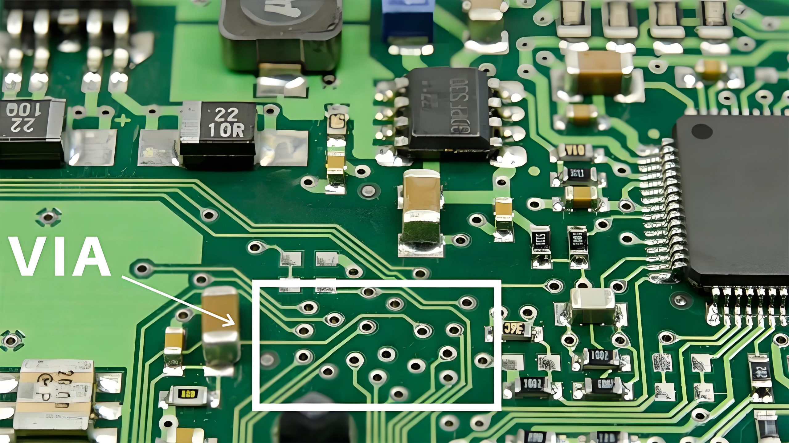
  • PTH: The hole wall is plated and is usually used for electrical connections, such as vias (VIA) and component holes. There is copper on these hole walls, which can achieve electrical conduction between the layers of the circuit board.
  • NPTH: The hole wall is not plated and is usually used for positioning, fixing and other functions, such as screw holes or connector fixing holes. There is no copper in these hole walls and does not participate in electrical connections.

2. Appearance characteristics:

  • PTH: There are traces of plating, the hole wall is smooth and covered with copper.
  • NPTH: There are no traces of plating, the hole wall is not smooth and not covered with copper.

3. Application scenarios:

  • PTH: Mainly used in scenarios where electrical connection is required, such as connecting different layers of a circuit board or connecting components.
  • NPTH: Mainly used in scenarios where electrical connection is not required, NPTH holes usually do not have hole rings, but in some special cases, hole rings are also designed to achieve grounding functions.

What is a PTH pad?

PTH pads (Plated Through Hole) refer to pads with through holes, and the hole walls are copper-plated. PTH pads play an important role in PCB design, and are mainly used to connect different layers of a circuit board or connect component pins to a circuit board.

The following points should be noted during the design and manufacturing process of PTH pads:

  • Size and shape: The outer ring of the PTH pad cannot be less than 0.2mm (8mil) on one side to ensure stability during welding.
  • Welding process: During welding, the PTH pad will take away a considerable amount of solder, which may cause insufficient solder problems.
  • Manufacturing capability: The design of the PTH pad is directly related to the manufacturing capability of the circuit board, which may cause welding quality problems.

PTH pads play a key role in PCB assembly, ensuring stable connection of components and reliable electrical performance. Correct PTH pad design can significantly improve the reliability and manufacturing quality of the circuit board.

How thick is plated through-hole plating?

The plating thickness standards for plated through-holes vary depending on the application scenario. Specifically:

  • IPC Level 1: The smallest thickness, short service life, usually used in consumer electronics that may become obsolete in a few years, requires an average thickness of 20 microns, and spots are not thinner than 18 microns.
  • IPC Level 2: More durable, continuously used holes, suitable for equipment that often runs for 5 years or more, requires an average thickness of 20 microns, and spots are not thinner than 18 microns.
  • IPC Level 3: The thickest and most durable plated through-holes, used for products expected to be used for ten years or more, requires an average thickness of 25 microns, and spots are not thinner than 20 microns.

What is the anatomy of a plated through-hole?

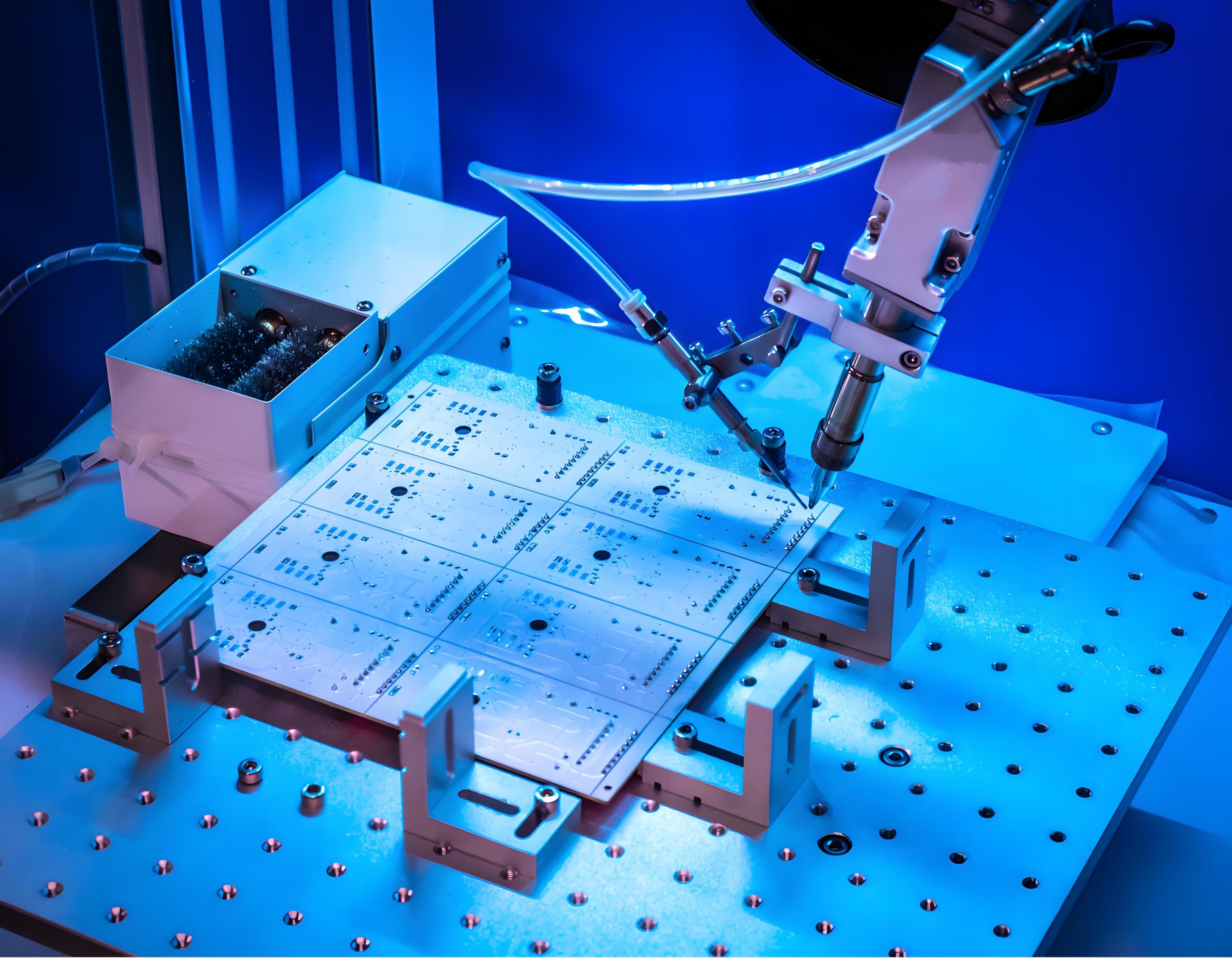
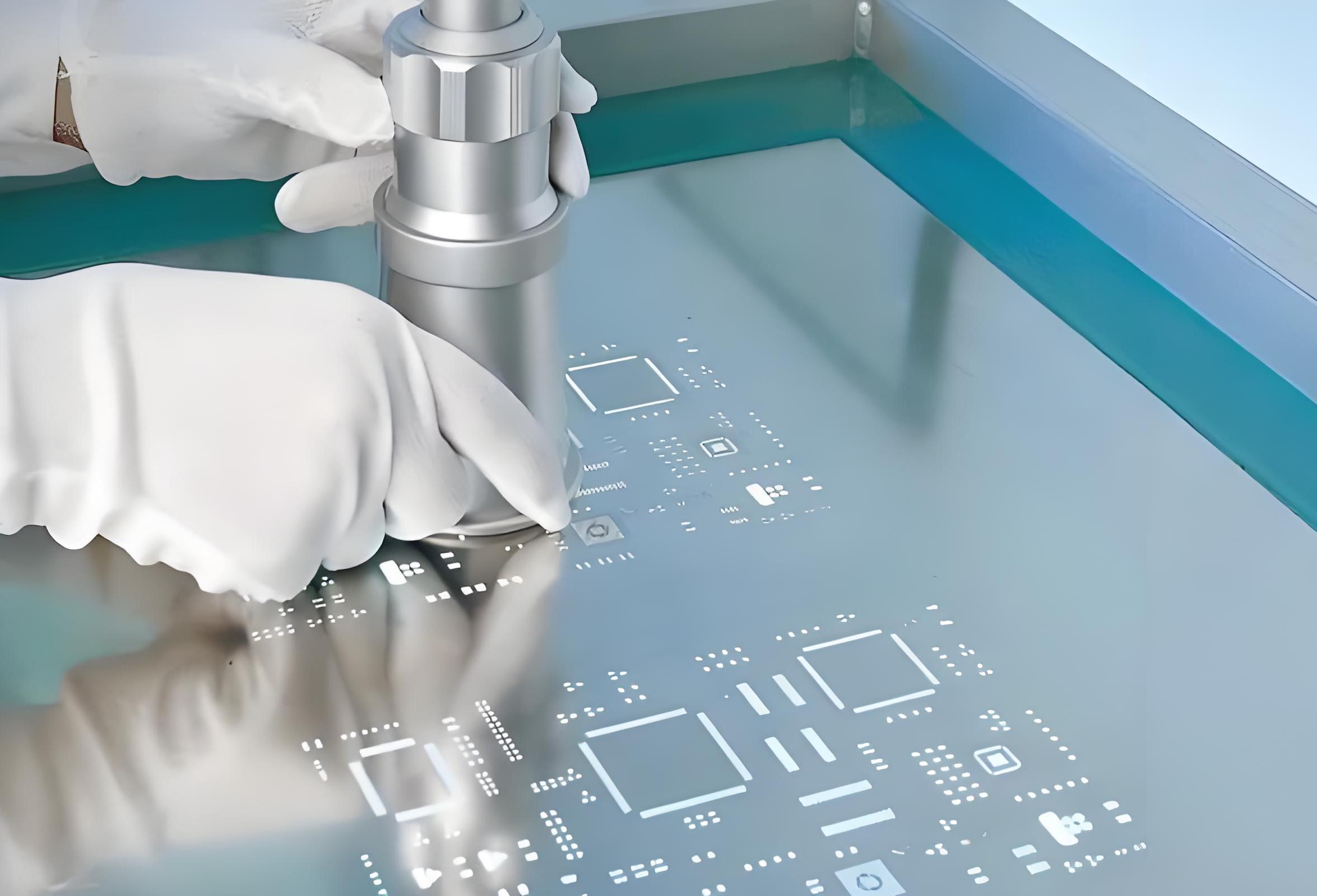
A plated through-hole (PTH) is a hole drilled in a circuit board, and a layer of metal is deposited on the hole wall through an electroplating process to achieve electrical connections between different layers of the circuit board. Its construction usually includes the following parts:

  • Hole wall: The hole wall of the plated through-hole is formed by drilling, usually in a circular or other shape.
  • Metal plating: A layer of metal deposited on the hole wall by electroplating process to achieve electrical connection. The thickness and quality of the metal plating have an important impact on the electrical performance and reliability of the plated through-hole.
  • Pad: Located at both ends of the plated through-hole, it is used to solder electronic components or connect other circuit boards. The shape and size of the pad are usually designed according to the type and size of the electronic component.
  • Solder mask: A layer of insulating material covering the surface of the circuit board to prevent solder flow and short circuit during soldering. The solder mask usually leaves a certain opening around the plated through-hole to solder electronic components.

What is the required hole fill of a plated through-hole?

The required hole fill of a plated through-hole is usually required to reach 100%. Specifically, the plated through-hole (PTH) should be filled with 100% vertical solder, the solder side should have a perfect fillet, and the component and pad should be in 100% contact with the solder.

The surface of the weld should be smooth, non-porous, non-disturbed, bright, and the solder joints completely wrap the solder feet and are concave. In addition, electroplating hole filling technology also plays an important role in improving the electrical performance and connection reliability of circuit boards.

What is NPTH in PCB?

Electroplating hole filling can improve electrical performance, improve connection reliability, avoid electromagnetic interference, and has excellent solderability and a more simplified process. In practical applications, electroplating hole filling is suitable for blind holes with a diameter of 80-220um and a thickness-diameter ratio of less than or equal to 1:1. The hole filling rate can reach more than 85%.

What is the difference between plated and coated?

The main difference between plating and coating lies in their formation method and application scenarios.

1. Formation method

  • Plating: Plating is a metal protective layer formed on the surface of the material by electroplating or chemical plating. Electroplating is to use the principle of electrolysis to plate a thin layer of other metals or alloys on certain metal surfaces to form a metal film. Chemical plating is to form a metal coating on the surface of the material through chemical reaction.
  • Coating: Coating is a protective layer formed by spraying paint on the surface of the material. Common coating methods include hot-dip galvanizing, thermal spraying and surfacing, which mainly apply metal to the surface of the substrate by physical means.

2. Application scenarios

  • Plating: Plating is widely used in aviation, automobile, electronics and other fields. In the aviation field, coating can improve the mechanical strength and processing accuracy of parts and reduce the weight of parts; in the automotive field, coating can improve the corrosion resistance and wear resistance of the car body.
  • Coating: Coating is widely used in construction, machinery, automobile and other fields. In the construction field, coating mainly plays the role of anti-corrosion, waterproof, heat preservation, etc.; in the mechanical field, coating can enhance the hardness, wear resistance and corrosion resistance of the material surface.

3. Advantages and disadvantages

  • Plating: Advantages include good anti-corrosion, anti-wear, electrical conductivity, thermal conductivity and aesthetics. Disadvantages are complex process and high cost.
  • Coating: Advantages are simple process, low cost, anti-corrosion, waterproof, wear resistance, heat insulation and other characteristics. Disadvantages are that the aesthetics and some physical properties are not as good as plating.

Although NPTH in PCB does not directly participate in electrical connection like plated through holes, it plays an irreplaceable role in mechanical installation, heat dissipation, etc., and together with plated through holes, it constitutes a complete functional system of PCB.

You may also like

What are PCB stencil printers?
Wednesday, December 18th, 2024

What are PCB stencil printers? stencil pcb printers is a process for applying solder paste to specific pad locations on a PCB board with high precision. The core tool is the PCB stencil, a thin sheet of precision-machined metal with holes that exactly match the shape, size, and location of the PCB board pads.

What is a PCB stencil?

A stencil in PCB refers to a tool used in the surface mount assembly process to precisely deposit solder paste at specific locations on a printed circuit board. The stencil is usually made of brass or stainless steel and is engraved with circuit patterns that match the locations of surface mount devices (SMDs) on the PCB.

What are PCB stencil printers?

The stencil plays a vital role in the PCB assembly process. It ensures that solder paste is accurately deposited at the locations of the SMDs, thereby ensuring that the components are accurately mounted in the correct locations.

The design of the stencil, including its composition, thickness, and the shape and size of the holes, will affect the quality of the solder paste deposition. Too much or too little solder paste can lead to welding quality problems, such as ball formation, bridging or tombstoning.

What is a PCB stencil made of?

PCB stencils are mainly made of stainless steel, which has good corrosion resistance and high hardness. This stencil is usually called a SMT Stencil or a solder paste printing stencil, which is mainly used to print solder paste onto PCB circuit boards during SMT assembly.

The stencil is cut by high-precision laser, and has holes or grooves corresponding to the PCB pads, which are used to accurately control the printing of solder paste.

What types of PCB stencils are there?

The types of stencil in PCB stencils mainly include the following:

  • AI stencil: mainly used in SMT process, can replace dispensing machines, improve production efficiency and reduce costs.
What are PCB stencil printers?
  • Laser stencil: through high-energy laser cutting to create an opening that perfectly matches the PCB pad, it has the advantages of high precision and smooth edges, and is particularly suitable for high-density and high-demand PCB assembly.
  • Etched stencil: The opening is formed by chemical etching liquid corroding the steel sheet. The cost is lower, but the accuracy and edge smoothness are not as good as laser cutting.

These stencil types have their own characteristics and are suitable for different PCB manufacturing needs. Laser stencils are particularly suitable for high-density and high-demand PCB assembly due to their high precision and smooth edges; while etched stencils are suitable for applications with low precision requirements due to their low cost and simple manufacturing process.

What is the function of a PCB stencil?

The stencil in the PCB template plays a vital role in the manufacturing process. The stencil is a high-strength metal grid that is mainly used to apply solder paste on the PCB. Its specific functions include:

  • Accurate quantitative distribution of solder paste: The stencil accurately controls the distribution of solder paste through the holes on it, ensuring that the solder paste is evenly and accurately applied to the predetermined pad position on the PCB, avoiding too much or too little solder paste, thereby ensuring welding quality.
  • Improve welding quality: By precisely controlling the distribution of solder paste, stencil helps reduce welding defects such as bridging and empty soldering, improves the consistency and reliability of welding, and thus improves the electrical performance of the entire PCB and the overall quality of the product.
  • Adapt to complex designs: With the trend of miniaturization and high density of electronic products, the components on PCBs are getting smaller and smaller, and the spacing is getting closer and closer. Stencil can be customized according to design requirements to meet the needs of high-end electronic products.
  • Improve production efficiency: On an automated production line, with the use of precision stencil and automatic solder paste printers, fast and efficient mass production can be achieved, greatly improving production efficiency and reducing the error rate of manual operation.

How to design a PCB stencil?

In the surface mount (SMT) assembly process, solder paste stencil plays a key role. Its ability to accurately apply solder paste is directly related to the quality and reliability of the connection between SMD components and PCB pads. The following are the key points to focus on when designing solder paste stencils:

  • Matching design files: The design of solder paste stencils must be closely constructed based on the solder paste layer information of the PCB to ensure that every hole and shape on the stencil is precisely matched with the solder paste layer, so as to provide an accurate basis for subsequent solder paste coating and avoid poor welding problems caused by design deviations.
  • Selection and thickness: There are many types of solder paste stencils, the most common of which are stainless steel stencils and polymer stencils. At the same time, the determination of stencil thickness cannot be ignored. It is usually in the range of tens to hundreds of microns. It needs to be finely adjusted in combination with factors such as pad size, pin spacing, and required solder paste amount to ensure uniformity and stability of solder paste coating.
What are PCB stencil printers?
  • Hole size and shape: The hole size and shape of the stencil should be perfectly matched with the solder paste area on the solder paste layer, and the solder paste coating range should be strictly controlled to prevent the solder paste from overflowing to the adjacent pads and causing short circuit failures, or insufficient solder paste coating affecting the welding quality, to ensure that the solder paste coating is accurate at every location.
  • Customized special design: For special components or parts with special pin structures, a special design scheme is required on the solder paste stencil.

How to use a PCB stencil?

The following are the steps to use a PCB stencil:

1. Preparation:

  • Check whether the PCB stencil opening is blocked or deformed, and whether the PCB board surface is clean.
  • According to the size of the printer and the stencil, install the stencil through the positioning hole and the printer positioning pin to ensure the correct direction and secure fixation.
What are PCB stencil printers?

2. Solder paste preparation:

  • Select solder paste according to PCB welding requirements and component type, check the shelf life and quality, take it out and stir it for 3-5 minutes to make it uniform.

3. Solder paste printing:

  • According to the thickness of the stencil, opening and solder paste characteristics, adjust the parameters such as the printer scraper pressure, printing speed), demolding speed and stroke.
  • Start the printer, and the scraper moves to fill the stencil opening with solder paste and transfer it to the PCB pad. Observe the printing situation during the process and adjust it in time if there is any problem.

4. Post-printing inspection and cleaning:

  • Use a magnifying glass or SPI to check the quality of solder paste printing on the PCB board, and reprint the unqualified ones after cleaning.
  • Use special solvents and tools to clean the template, remove the residual solder paste, and store it properly after drying.

PCB stencil printing is an indispensable key process in the field of electronic manufacturing. As a core tool, the quality and precision of the stencil directly determine the coating effect of the solder paste on the PCB board, which in turn affects the welding quality of electronic components, and ultimately plays a decisive role in the performance, reliability and stability of electronic products.

You may also like

How are the circuit boards connected?
Tuesday, December 17th, 2024

How are the circuit boards connected? Soldering is the most common and long-standing way to connect circuit boards. For traditional circuit boards, we usually use electric soldering irons to perform soldering operations. First, the metal part of the electronic component pins or wires to be connected is tightly fitted with the corresponding pads on the circuit board. Then, the pads and pins are heated with an electric soldering iron, and the solder wire is brought close together to melt the solder and evenly wrap the connection parts to form a stable metal connection.

How are the circuit boards connected?

A circuit board 6 connections typically refers to a design that incorporates six distinct points or pads for electrical connections, which could be input/output ports, signal pathways, or power connections. These boards are often used in simple applications where a limited number of connections are needed to interface with other components or systems.

What are the connections between circuit boards?

The main ways to connect circuit boards include the following:

  • Welding connection: This is one of the most commonly used connection methods, which connects components on the circuit board together by welding. The advantages of welding connection are stable and reliable connection, low cost, and suitable for circuit boards that do not require regular changes.
  • Plug-in connection: Plug-in connection can achieve fast plug-in and pull-out, easy replacement and maintenance, but requires high precision of plug-ins and sockets, and occupies a large space, which is not suitable for circuit boards with limited space.
  • Connector connection: This is a widely used circuit board connection method that can connect circuit boards of different forms and sizes. The advantages of connectors are convenient and fast connection, high reliability, and a large number of plug-in and unplug times, which are suitable for various circuit board application scenarios.
  • Plug-in connection: widely used in complex instruments and equipment, and connected through standard pins or sockets. This method is easy to replace and repair, ensuring the reliability and production efficiency of the connection.
  • Special connection methods: including V-cut and copper foil bridge connection, spring connection and spring connection, panel connection, etc. These methods are suitable for specific scenarios and needs, such as V-cut for the separation stage of PCB boards, spring connection and spring connection for the connection of flexible circuit boards, and panel connection for multiple PCB designs placed on a large substrate.

How to connect components on PCB?

There are usually the following ways to connect components on PCB:

  • Soldering: This is the most common connection method. By connecting the pins of the components to the pads on the PCB with solder, you can use a soldering iron or SMT equipment for soldering.
  • Spring contact: For some components that need to be replaced frequently, such as batteries, you can use spring contact to make the components easy to disassemble.
How are the circuit boards connected?
  • Screw fixing: For components that need to withstand large forces, such as heat sinks, motors, etc., screw fixing can be used. Pay attention to choosing the right screws and tightening strength.
  • Clamping with pliers: For some components that need to be fine-tuned, such as rheostats, potentiometers, etc., pliers can be used to clamp.
  • Plastic bayonet: For some components that need to be frequently plugged and unplugged, such as wire connectors, plastic bayonet can be used for connection.

How to connect PCB boards together?

To connect PCB boards together, you can consider the following common methods:

Welding:

  • PCB wire welding: This is a simple and commonly used method to achieve connection by directly welding the wire to the pad of the PCB board. When welding, you need to pay attention to the quality and stability of the welding to ensure the reliability of the connection.
  • PCB cable welding: It is suitable for situations where multiple wires need to be connected. You can use cable to connect multiple PCB boards together, and then fix the connection between the cable and the PCB board by welding.
  • Direct welding between PCBs: This method is often used for connections between two PCB boards at a 90-degree angle. When welding, attention should be paid to the alignment and fixation between the two PCB boards to ensure the quality of welding.

Plug-in connection:

  • Printed circuit board socket: This connection method is often used in more complex instruments and equipment. A printed plug is made from the edge of the PCB board. The plug part is designed according to the size of the socket, the number of contacts, the distance between contacts, the position of the positioning holes, etc., so that it matches the dedicated PCB printed circuit board socket.
How are the circuit boards connected?
  • Standard pin connection: This method is suitable for use in small instruments. Two PCB boards are connected by standard pins. The two PCB boards are generally parallel or vertical.
  • Crimping: The PCB board is crimped with other components through a special crimping tool to achieve connection. This method is suitable for situations where frequent disassembly and replacement are required.
  • Bonding: Use glue or adhesive to bond the PCB board with other components. This method is suitable for situations where the connection strength requirement is not high.
  • Use connectors: Connectors are a component specially used to connect PCB boards, which can provide reliable connection and convenient disassembly. There are many types of connectors, and you can choose the right connector according to specific needs.
  • Screw fixing: For some larger or heavier PCB boards, screws can be used to fix them to other components to ensure the stability of the connection.

What are the different types of PCB connectors?

The main types of PCB connectors include the following categories:

  • Ordinary board-to-board connector: used to connect two parallel or vertical PCBs, suitable for signal transmission between different circuit boards. According to different spacing, it can be divided into 0.50mm, 0.60mm, 0.80mm and other specifications. The smaller the spacing, the more pins can be accommodated, and the signal transmission is more intensive, but the processing accuracy and installation requirements are higher.
  • Mezzanine connector: mainly used to connect two PCBs with close spacing when space is limited. It is usually connected in a stacked manner to save space and is often used in the connection structure of the motherboard-daughterboard.
  • Backplane connector: a group of electrical connectors parallel to each other, each pin of each connector is connected to the same relative pin of all other connectors to form a connector bus.
  • Spring-type board-to-board connector: contains a spring structure inside, which can ensure a stable connection even when the spacing between the boards fluctuates. It is suitable for devices with high requirements for connection stability.
  • Wire-to-board connector: used to connect wires or cables to PCBs. The wire connection part is similar to the wire-to-wire connector, while the circuit board connection part is mostly a two-piece connector that is press-fit or welded.
  • Wire-to-wire connector: used to connect two wires. One end of the connector is permanently connected to the wire, and the other end forms a detachable interface. Permanent connection methods can use crimping or insulation displacement contacts (IDC), etc.

How to choose PCB connectors?

There are several key factors to consider when choosing PCB connectors:

  • Connector type: choose the appropriate connector type according to application requirements.
  • Size: The size of the connector needs to adapt to the size and layout of the circuit board to ensure that the connector can be properly installed and connected.
How are the circuit boards connected?
  • Electrical performance: consider the rated voltage, rated current, and withstand voltage of the connector to ensure that it can withstand the electrical load required by the device.
  • Mechanical performance: includes the number of plug-in and unplugging times, durability, and shock resistance. If the device needs to frequently plug and unplug the connector, a durable and long-life connector should be selected; if the device will be subject to vibration or shock, a connector with good shock resistance should be selected.
  • Environmental conditions: Environmental conditions have a great impact on the choice of connectors.
  • Technical parameters: Understand the technical requirements of the application, including pin spacing, soldering method, rated voltage, rated current, number of plug-in and unplug times, temperature range, board spacing, connector geometry, and solder hole diameter of the solder tab.

How do you connect wire to a circuit board?

Soldering is usually used to connect wires to circuit boards. Solder the ends of the wires to the pads on the circuit board using a soldering iron and solder.

  • Prepare tools and materials: soldering iron, solder wire, flux, wires, and circuit boards.
  • Clean wires and circuit boards: Use alcohol or other cleaning agents to clean the wires and pads on the circuit board to ensure a good solder connection.
  • Strip the wire: Use wire strippers or scissors to strip a section of the wire end to expose the metal wire inside.
  • Tin the wire: Place the end of the wire on the soldering iron tip and wrap it with solder wire at the same time to evenly coat the end of the wire with a layer of solder.
  • Solder wires to circuit boards: Place the tinned wire ends on the pads on the circuit board, and use a soldering iron to melt the solder to connect the wires to the pads.
  • Check welding quality: Check whether the solder joints are firm and whether there are problems such as cold solder joints or short circuits.
  • Clean the soldering area: Use alcohol or other detergents to clean the soldering area to remove excess solder and flux.

Circuit board connection is a technology that requires both theoretical knowledge and practical experience. From basic soldering and plug-in connections to various unique ways of PCB connection, each connection method has its applicable scenarios and key points. Regardless of the connection method, preparation before connection, detailed control during the connection process, and detection and debugging after connection are all crucial.

You may also like

What is heavy copper pcbs?
Friday, December 13th, 2024

What is heavy copper pcbs? That is, the copper foil thickness is greater than the conventional standard PCB. Generally speaking, when the copper foil thickness reaches 3 ounces per square foot (oz/ft²) and above, it can be called a heavy copper PCB.

The manufacturing process of heavy copper PCBs is more complicated than that of ordinary PCBs, requiring higher technical levels and professional equipment. Compared with ordinary PCBs, its characteristics are high current carrying, good heat dissipation, high mechanical strength and strong reliability. It is suitable for high-power electronic equipment, harsh working environments and fields with high reliability requirements.

What is heavy copper pcbs?

What is high copper thickness PCB?

High copper thickness PCB refers to a printed circuit board that uses thicker copper foil as the conductive material. In the standard PCB manufacturing process, the thickness of the copper foil is usually determined according to the application requirements, but when the thickness of the copper foil is greater than or equal to 3 ounces, this PCB is called a high copper thickness PCB.

Usually compatible with FR-4 dielectric, mainly used for inner layers rather than outer layers, plated through holes (PTH) usually need to be plugged/filled, and careful registration and lamination are required

Common heavy copper PCB thickness:

  • 2 oz (70 microns)
  • 3 oz (105 microns)
  • 4 oz (140 microns)
  • 6 oz (210 microns)
  • 8 oz (280 microns)
  • 10 oz (350 microns)

Application areas of heavy copper PCB:

  • Automotive electronics: widely used in key electronic devices such as automotive control modules, engine control systems, airbags, etc., because they can withstand high temperature, low temperature, corrosion and other environmental factors.
  • Power circuit: widely used in power modules, DC-DC converters and high power distribution boards, etc., capable of handling high current and high power requirements.
  • Industrial control system: used in high power motor drives, automation equipment and large mechanical control to meet the needs of high conductivity and mechanical strength.
  • Renewable energy systems: used in solar and wind energy systems to ensure stable system operation and reduce failure rates.

What are the advantages of heavy copper PCBs?

  • High conductivity: High copper PCB uses heavy copper foil as the conductive layer. Compared with ordinary PCB, its conductivity is significantly improved, which can carry larger current, reduce resistance loss and improve circuit efficiency.
  • High mechanical strength: Due to the increase in the thickness of copper foil, the mechanical strength of high copper PCB is also improved accordingly, which can withstand greater mechanical stress and impact, and is not easy to deform or damage.
What is heavy copper pcbs?
  • Good heat dissipation performance: High copper PCB can quickly transfer heat from the circuit to the surrounding environment, effectively prevent components from overheating and damage, and improve the reliability and service life of the equipment.

What type of copper is PCB?

There are mainly the following types of copper on PCB: red copper, copper clad plate and inner layer copper.

  • Red copper: Red copper is the earliest material used in circuit boards, and is widely used due to its good processing performance and conductivity. The main component of red copper is copper, and the other components are less, but the disadvantage is that it is easily oxidized and corroded.
  • Copper clad laminate: Copper clad laminate is a layer of copper foil on an inorganic substrate, usually used for double-sided and multi-layer circuit boards. The copper foil ensures the conductivity and connectivity of the circuit board, while the inorganic substrate provides mechanical strength and heat resistance.
  • Inner copper: Inner copper is used in multi-layer circuit boards, which are made of multiple layers of inorganic substrate and copper foil. It is usually used in high-density or high-speed design circuit boards, with better signal transmission performance and higher mechanical strength, but the manufacturing cost is higher.

In addition, there are different types of copper foil in PCB, including electrodeposited copper and rolled copper. Electrodeposited copper has a vertical grain structure and a rougher surface, which is suitable for rigid PCB boards; while rolled copper has a horizontal grain structure and a smoother surface, which is suitable for flexible and high-speed circuit boards.

How thick is 2 oz copper on PCB?

The thickness of 2 oz copper is about 70 microns. In PCB design, copper thickness is usually expressed in ounces (oz), and the thickness of 1 ounce of copper is about 35 microns, so the thickness of 2 ounces of copper is about 70 microns.

The copper thickness standard of PCB board is usually expressed in oz/ft² (ounces/square foot) or um (micrometer). The copper thickness of PCB board has an important impact on the performance and stability of the circuit board. The outer copper thickness mainly affects the stability of signal transmission and the ability to resist electromagnetic interference, while the inner copper thickness affects the signal transmission rate and signal-to-noise ratio.

Generally speaking, the thicker the outer copper thickness, the stronger the stability and signal strength of the circuit board, which is suitable for high-frequency and high-speed occasions; while the thinner the inner copper thickness, the more suitable for high-speed transmission signals, and the thicker the inner copper thickness, the more suitable for low-speed transmission signals and high signal-to-noise ratio signals.

Why use heavy copper PCB?

The main reasons for using heavy copper PCB include the following aspects:

  • Enhanced current carrying capacity: Heavy copper PCB uses a thicker copper layer, which can carry a larger current and reduce resistance and voltage drop. This is especially important for high-power applications or circuits that require high current transmission.
  • Optimize heat dissipation performance: Copper has good thermal conductivity, and a thicker copper layer can more effectively conduct heat away from hot spots and improve heat dissipation efficiency.
  • Improve signal transmission efficiency: Thicker copper layers can reduce losses and reflections during signal transmission and improve signal integrity.
  • Enhance mechanical strength: Thicker copper layers can increase the overall structural strength of PCBs, making them more resistant to physical shock and deformation.
  • Adapt to complex process requirements: Heavy copper PCBs can meet complex circuit design requirements through special process treatments, such as etching, drilling, gold plating, etc., to ensure the accuracy and reliability of circuit boards during manufacturing.

What is the most common copper thickness for PCB?

The most common PCB copper foil thickness is 35 microns. This thickness of copper foil is suitable for most consumer electronics products, can meet daily current and heat requirements, and has a relatively low cost and is suitable for large-scale production.

How are heavy copper PCBs made?

In the initial stage of making heavy copper PCBs, relatively heavy copper foil materials are selected. These copper foils are usually produced by electrolytic copper. During the electrolysis process, copper foils of different thicknesses can be produced by controlling the conditions of electrolysis, such as current density, electrolyte composition, and electrolysis time.

For situations where thicker copper foil is required, multiple lamination methods are used. Multiple layers of copper foil and insulating substrate materials are laminated according to design requirements, and then the copper foil and substrate are tightly combined through a high-temperature, high-pressure lamination process.

Next, the circuit pattern is manufactured on the outer layer of the heavy copper PCB, usually using a photolithography process. After that, according to the design requirements, holes are drilled on the heavy copper PCB to provide conditions for installing components and connecting circuits.

What is heavy copper pcbs?

After the drilling is completed, a metal layer is covered on the hole wall using electroplating technology to achieve a connection between the layers, and a layer of copper foil is electroplated on the hole wall to increase the thickness of the conductor and the surface pad. Next, the dry film and excess copper foil are removed, and chemical etchants are generally used to make the circuit pattern clearer.

Subsequently, the heavy copper PCB is subjected to surface treatment, such as gold plating, tin spraying, etc., to improve welding performance and corrosion resistance. Finally, the finished heavy copper PCB is strictly inspected and tested to ensure that its electrical and mechanical properties are consistent with the design requirements.

Professional Heavy copper PCB manufacturers – BEST Technology

The minimum width and thickness of the heavy copper PCB conductor are mainly determined based on the required current carrying capacity and the maximum temperature rise allowed for the conductor. From the perspective of its size specifications and actual manufacturing process, the routing of the circuit board may not be a regular rectangular shape.

What is heavy copper pcbs?

It is worth noting that the thicker copper conductor will significantly increase the overall thickness of the circuit board to a large extent. In terms of manufacturing process, the additive method (electroplating) process has certain advantages over the subtractive method (etching) process, but at the same time, its cost is relatively higher.

BEST Technology process capabilities:

  • Substrate: FR4/Aluminum
  • Copper thickness: 4OZ~10OZ
  • Extremely heavy copper thickness: 20~200 OZ
  • Contour: Milling, Punching, V-Cut
  • Solder mask: White oil/Black oil/Blue oil/Green oil/Red oil
  • Surface treatment: Immersion gold, tin spraying, OSP
  • Maximum panel size: 580*480mm(22.8″*18.9″)

Heavy copper PCB occupies an important position in the electronics field with its unique characteristics. With high current carrying capacity, good heat dissipation performance, higher mechanical strength and excellent reliability, it has become an ideal choice for many high-demand application scenarios. From power electronics to automotive electronics, from aerospace to medical equipment and communications, heavy copper PCB plays a key role.

You may also like

How to make two sided pcb in Altium?
Friday, December 13th, 2024

How to make two sided pcb Altium? Be familiar with the interface and basic operations of Altium Designer, accurately design the circuit schematic diagram, reasonably plan the PCB layout, make full use of the double-sided space, conduct fine wiring, ensure signal integrity, and correctly set the rules and parameters to meet production requirements.

How to make two sided pcb in Altium?

What is a double-sided PCB?

Double-Sided PCB refers to a printed circuit board with conductive copper layers on both sides, and the circuit between the two sides is connected through through holes (small holes). This design enables double-sided PCBs to implement more complex circuit layouts in limited space without significantly increasing the board size.

Double-sided PCBs are widely used in various application scenarios that require complex circuit layouts and high-density assembly, such as computers, communication equipment, industrial control, and consumer electronics.

Because it can achieve more complex circuit designs in a limited space, double-sided PCB is particularly suitable for applications that require higher-function electronic equipment, such as smart home equipment, computer hardware, medical equipment, etc.

How to make two sided pcb in Altium?

Here are the general steps for making a double-sided PCB in Altium:

  • Create a project: In Altium Designer, select “File” > “New” > “Project” to create a new PCB project.
  • Draw a schematic: Select “File” > “New” > “Schematic” to create a new schematic file. Add the required components to the schematic and connect them using wires.
  • Add package library: If you need to use a custom package library, you need to add it to the project. Select Design > Add/Remove Library and select the desired footprint library.
  • Generate PCB: After the schematic is drawn, select “Design” > “Update PCB Document” to import the components and connection information in the schematic into the PCB.
  • Layout components: In PCB, components are laid out according to design requirements. You can use Altium’s automatic layout tools or manual layout.
How to make two sided pcb in Altium?
  • Routing: Use Altium’s routing tools to route the connections between components. You can choose automatic routing or manual routing.
  • Add silkscreens and logos: Add silkscreens and logos to the PCB to easily identify components and connections.
  • Check and Validate: Use Altium’s Design Rule Checker tool to check that your PCB design meets requirements. Electrical rule checks, wiring rule checks, etc. can be performed.
  • Generate manufacturing files: After the PCB design is completed, select “File” > “Fabrication Outputs” to generate manufacturing files, such as Gerber files, drilling files, etc.

How to make two-sided PCB?

After designing the layout of the double-sided PCB in the PCB design software according to the circuit schematic diagram, the production process begins.

The complete process of making double-sided PCB:

  • Preparation materials: Choose a copper-clad laminate covered with copper foil of a specific thickness (such as 18μm, 35μm, etc.) on both sides, and determine the copper foil specifications according to circuit requirements.
  • Drilling: According to the drilling documents, use a CNC drilling machine to drill high-precision holes to ensure the connection paths for the circuits on each layer.
  • Copper immersion: Place the drilled PCB board in a copper immersion liquid to deposit a thin copper layer on the hole wall, laying the foundation for subsequent copper electroplating and ensuring the reliability of electrical connections.
  • Copper electroplating: Use the PCB board as the cathode to energize the copper ion plating solution, thicken the copper layer to the design standard, and enhance the electrical conductivity and mechanical properties.
  • Exposure and development: The Gerber file is made into a film. After applying photoresist to the copper-clad board, the film pattern is printed on the board through exposure equipment, and then the unexposed photoresist is dissolved with a developer to initially present the circuit pattern.
  • Etching: Use ferric chloride or acidic etching solution to dissolve the copper foil that is not protected by the photoresist, and form precise lines on both sides of the copper-clad board. Then use a film stripping solution to remove the remaining photoresist.
  • Make the solder mask layer: Use screen printing to apply solder mask ink of the selected color on the circuits on both sides of the board, and use screen printing to print white character ink on the corresponding positions of the cured solder mask layer to mark component information to facilitate assembly and debugging.
  • Drying treatment: Drying fixes the character ink to avoid fading and blurring.
  • Surface treatment: Dip tin or spray to coat the pad with tin layer to improve solderability, suitable for products with regular soldering requirements.

Can you put components on both sides of a PCB?

Components can be placed on both sides of the PCB. Both sides of the PCB double-sided panel can be wired and components placed, which can reduce the difficulty of wiring and is suitable for the design of complex circuits.

How to make two sided pcb in Altium?

In a double-board design, larger and denser components such as QFP and BGA are usually placed on the top layer of the board, while plug-in components can only be placed on the top layer. Smaller components and components are placed on the other side (bottom layer) of the plug-in components. Chip components with a small number of pins and loose arrangement.

How do you flip a PCB in Altium?

Use the shortcut key: Press the “V” key and then the “B” key to quickly flip the PCB view to the bottom layer. This method is like turning the PCB board over visually, making it easier to view the underlying component layout, wiring, etc.

Operation through the menu: Select the “View” menu, find the “Flip Board” option in the drop-down menu, and click it to flip the PCB view between the top and bottom layers. This method is relatively intuitive and suitable for users who are not familiar with shortcut keys.

How do you flip a component to the bottom in Altium?

Menu operation: Hold down the “Ctrl” key and use the left mouse button to click the components that need to be flipped one by one to select them all. Then follow the menu operation steps for flipping a single component, that is, select “Edit” – “Move” – ​​”Flip Selection”, so that multiple selected components can be flipped to the bottom together.

Shortcut key operation: First select multiple components, the selection method is the same as above, also hold down the “Ctrl” key and click the components. Then press the “L” key to flip these selected components to the bottom layer at the same time.

How do I mirror graphics in Altium?

In the schematic editing environment, select the component that needs to be mirrored. You can select it by left-clicking the component with the mouse. Then select the “Edit” menu and click on the “Mirror” option. Or use the shortcut key “Ctrl + M” to mirror the component in the horizontal direction. Properties such as the pin connections of the component will not change, only the graphic appearance will be mirrored.

How to make two sided pcb in Altium?

In the PCB editing environment, select the component to be mirrored by clicking it directly with the left mouse button. Select the “Move” submenu under the “Edit” menu and click on the “Mirror Selection” option. The component will be mirrored with the axis perpendicular to the PCB board plane as the axis of symmetry. This is useful when adjusting component layout, especially when you need to flip the component from top to bottom and mirror it at the same time, etc.

In addition, for some regularly shaped components (such as rectangular components), you can also select the component and hold down the “L” key to achieve the effect of flipping and mirroring the component between layers.

How do I rotate a whole PCB in Altium?

Use keyboard shortcuts to rotate in the PCB Editor:

Select the entire PCB (you can select the entire PCB through the “Edit” menu – “Select” – “All”). Press “Space” to rotate the PCB counterclockwise in 90° increments. This is a faster way to rotate, making it easier to adjust the direction of the PCB during the layout and routing process to better fit the workspace or meet specific layout ideas.

Rotate via menu options:

Also select the entire PCB first. Select the “Edit” menu – “Move” – ​​”Rotate Selection”. In the pop-up dialog box, you can set the rotation angle. The PCB can be rotated accurately according to the design requirements, such as inputting any angle such as 45°, 60°, etc., and then clicking the “OK” button to complete the rotation operation. This method is relatively more flexible and can meet the rotation needs of non-integer multiples of 90°.

During the design process, pay attention to key points, be familiar with the operation of the software, accurately design the circuit schematic, reasonably plan the PCB layout, conduct fine wiring, set correct rules and parameters, and conduct strict inspection and optimization. Only in this way can the quality and reliability of PCB design be ensured and meet the needs of practical applications.

You may also like

What is the ffsd pcb connector?
Thursday, December 12th, 2024

What is the ffsd pcb connector? The FFSD PCB connector is a high-performance, high-reliability printed circuit board connector, usually used to connect flexible flat cables (FFC/FPC) and flexible printed circuits (FPC). The FFC/FPC cable connected by the FFSD connector has good flexibility, can bend and move in a small space, and can adapt to the connection requirements between circuit boards of different shapes and sizes.

What is a PCB connector?

The PCB connector is a connector specifically used to connect and fix printed circuit boards (PCBs). It usually adopts a pin press-in design with super strong FPC cable clamping force. It is mainly used for PCB board and board connection to ensure precise and reliable electrical connection.

What is the ffsd pcb connector?

In terms of classification, it is divided into plug-in type (convenient plug-in and replacement), crimping type (high reliability, suitable for vibration environment) and welding type (stable electrical performance, not easy to replace) according to the connection method; it is divided into power connector (transmitting power), signal connector (transmitting signals) and hybrid connector (transmitting power and signals at the same time) according to the purpose.

What is the ffsd pcb connector?

FFSD connector is a type of PCB connector with specific design, specifications and performance characteristics. FFSD connectors generally adopt specific contact systems and shell designs, with compact shells and unique locking devices, etc., to ensure the stability and reliability of the connection and adapt to its specific application scenarios and signal transmission requirements.

FFSD connectors are designed and developed for flexible connection with shielded flat cables. Its excellent characteristics enable it to perform well in environments with strict requirements for high anti-interference and compact layout, and can effectively connect flexible flat cables (FFC/FPC) and flexible printed circuits (FPC).

FFSD cables are mostly made of special flexible and anti-bending materials. The shielding layer on the surface can significantly reduce electromagnetic interference (EMI) in high-frequency environments, effectively ensure the stability and accuracy of signal transmission, and provide solid guarantees for the efficient and stable operation of various precision electronic equipment.

What is the structure of the ffsd pcb connector?

FFSD connectors are mostly designed with double-row pins, and the pin pitch is usually 0.050 inches (1.27mm), which can meet different signal transmission requirements. In addition, the number of pins generally ranges from 3 to 25, which can adapt to various circuit connection requirements.

The shell is generally made of insulating materials such as plastic, such as PBT, to provide mechanical support and protection for the connector, ensure the normal operation of the internal contact system, and enable the connector to be properly aligned and installed with other components. At the same time, the shell may also have some special designs, such as locking devices, which are used to fix the connector and the mating parts to prevent loosening or falling off during use.

What is the ffsd pcb connector?

The common installation method is cable installation, which connects the connector and the cable together through welding or crimping, and then connects the cable to the PCB board to achieve signal transmission. Some FFSD connectors may also support surface mount technology (SMT), directly soldering the connector on the surface of the PCB board to adapt to different circuit layouts and design requirements.

What are the most common PCB connectors?

Common PCB connectors include:

  • Pin-and-female connectors: They consist of a pin-and-female connector with metal pins and a female connector with a flexible metal sheet socket, used to connect between circuit boards or other components.
  • USB connector: There are many types such as Type-A and Type-B. The internal metal contact piece transmits power and data. It is widely used for data transmission and charging of computers, mobile phones and other devices.
  • HDMI connector: It contains multiple pins to transmit high-definition video and audio signals, has shielding measures, and is used to connect video sources and display devices.
  • SATA connector: It uses serial data transmission, has data and power interfaces, and is a key component for connecting hard disks, optical drives and motherboards in computers.
  • D-Sub connector (VGA connector): It is shaped like a “D”, and multiple pins transmit analog video signals. It is still used to connect computers and monitors in some old devices or low-resolution occasions.
  • RJ45 connector: It has 8 internal metal contacts, which are used for Ethernet connection. It is an important component for computer network card interfaces, router LAN interfaces, etc. to achieve wired network communication.

How to choose PCB connectors?

There are several key factors to consider when choosing PCB connectors:

  • Technical parameters: First, understand the technical requirements of the application, including pin spacing, welding method, rated voltage, rated current, number of plug-in and pull-out times, temperature range, board spacing, connector geometry, and solder hole diameter of the soldering lug.
  • Electrical performance: The electrical performance of the connector includes limiting current, contact resistance, insulation resistance, and dielectric strength.
  • Installation space: Pay attention to the outer dimensions and installation space of the connector to ensure that it does not interfere with other parts. Pay attention to the number of pins and spacing to avoid high temperature deformation during the soldering process of the SMT machine.
  • Packaging form: For automated assembly, the packaging form is also important. Common packaging forms include tape and reel packaging and strip boxes, the former is more suitable for mass production.

Suggestions for choosing different types of PCB connectors:

  • Pin and female headers: cheap and common, suitable for low-end, large-size devices. The advantages are cheap and convenient, and the disadvantages are large size and difficult to bend.
  • High-end board-to-board connectors: many pins, small size, suitable for compact products. The advantage is stable connection, the disadvantage is high price and cannot be plugged and unplugged frequently.
  • Thickened board-to-board connector: suitable for development boards and test boards, the advantage is cheap and easy to connect and measure, the disadvantage is large size and not suitable for mass production scenarios.
  • FPC connector: suitable for the connection between the main board and the sub-board, the advantage is small size and flexibility, the disadvantage is high price.

How does the ffsd pcb connector work?

The working principle of the ffsd pcb connector is mainly based on the design and manufacture of printed circuit boards (PCBs). PCB connectors are made of printed circuits and printed components or a combination of the two by pre-designing on insulating materials to achieve electrical connections between electronic components.

Specific working mechanism of PCB connectors

  • Electrical connection: The wires and metal lines on the PCB are used to connect electronic components. The electrical performance requirements of the circuit are met by laying out and designing the parameters such as the path, width and spacing of the wires.
  • Mechanical support: PCB provides mechanical support and fixation for electronic components, fixes components by welding, plug-in or surface mounting, and ensures the relative position and stability between components.
  • Signal transmission: The wires and circuit paths on the PCB are used to transmit signals in electronic devices, considering factors such as signal integrity, noise suppression and interconnection length to ensure stable signal transmission and reduce interference2.

PCB connectors include not only traditional pin connectors and terminal blocks, but also various forms such as SMT (surface mount technology) and BGA (ball grid array).

The design and manufacture of these connectors have improved the miniaturization, integration and reliability of electronic products. In practical applications, PCB connectors are widely used in various electronic devices as an important carrier for connecting, supporting and managing electronic components.

What are the advantages of ffsd pcb connector?

The advantages of FFSD PCB connectors mainly include the following points:

  • High flexibility and adaptability: The FFC/FPC cable connected by the FFSD connector has good flexibility, can bend and move in a small space, and can adapt to the connection requirements between circuit boards of different shapes and sizes.
  • Excellent anti-interference ability: The shielding layer on the surface of the FFSD cable can effectively reduce electromagnetic interference in high-frequency environments, ensure the stability and reliability of signal transmission, and enable the equipment to work normally in complex electromagnetic environments.
What is the ffsd pcb connector?
  • High reliability: The locking mechanism of the connector can firmly fix the cable to prevent it from loosening or falling off due to vibration, impact and other factors during use, ensuring the stability of the connection, thereby improving the reliability and service life of the entire electronic system.
  • Good electrical performance: It can meet the requirements of high-speed signal transmission, has low contact resistance and transmission loss, and ensures the integrity and accuracy of the signal.
  • High degree of customization: FFSD connectors can be customized according to specific application requirements, such as cable length, width, bending angle, number of connector pins, spacing, etc. can be designed on demand, which can better meet personalized connection needs.

What are the applications of ffsd pcb connectors?

FFSD PCB connectors usually refer to FFC/FPC PCB connectors, which are widely used, mainly in the following fields:

  • Consumer electronics: Connecting various components in smartphones and tablets to meet their small space, multi-function, and thin requirements, and ensure signal and power transmission.
  • Medical electronics: In monitoring, imaging, circuits and displays, it helps data acquisition and processing to meet the needs of small and portable equipment.
  • Industrial control: Connect key components in automated production lines and instrumentation to achieve signal interaction and coordination, and improve production and equipment performance.
  • Communication equipment: Connect related modules in base stations, optical communications, routers, etc. to ensure stable signal transmission and adapt to high-speed communication and anti-interference requirements.
  • Aerospace: Applied to avionics and satellite communication equipment to ensure stable signals and reliable operation of equipment in harsh environments, which is related to flight and communication safety.

As a high-performance and high-reliability electronic connection component, FFSD PCB connector plays an indispensable role in modern electronic devices. Its high flexibility, anti-interference ability, miniaturization, convenient assembly, high reliability, good electrical performance, high degree of customization and cost-effectiveness have made it widely used in consumer electronics, automotive electronics, medical electronics, industrial control, communication equipment, aerospace and other fields.

You may also like

What is PCB nickel plating?
Thursday, December 12th, 2024

What is PCB nickel plating? PCB nickel plating refers to a layer of nickel covering on the surface of the circuit board. Its main function is to enhance the corrosion resistance, resistivity and solderability of the circuit board, while improving signal transmission performance and reliability. The nickel plating layer can protect the surface of the circuit board, prevent diffusion between metals, and improve the mechanical strength and durability of the circuit board.

PCB finition nickel or électrolytique soudabilité refers to the finishing process used on PCB to enhance solderability and protect exposed copper surfaces. Nickel is often applied as an underlayer, providing a robust, corrosion-resistant base for further finishes. Electrolytic finishes, such as electroplated gold or tin, are added on top to improve conductivity, durability, and ease of soldering. These finishes ensure reliable component attachment, minimize oxidation, and support the long-term performance of the PCB in various environments. The choice of nickel or an electrolytic finish depends on the specific application requirements, such as thermal resistance, electrical performance, and mechanical stability.

What is PCB nickel plating?

What is the function of PCB nickel plating?

The main functions of PCB nickel plating include improving wear resistance, preventing metal diffusion, enhancing mechanical strength, and adapting to the requirements of hot pressure welding and brazing.

Nickel plating on PCB (Printed Circuit Board) can significantly improve the wear resistance of switch contacts, contacts or plug gold. At the same time, the nickel layer acts as a barrier layer, which can effectively prevent the diffusion of copper and other metals, thereby protecting the circuit board. performance and lifespan.

In addition, the nickel layer can also improve the mechanical strength of the gold layer, making it more suitable as a substrate coating for precious and base metals.

  • Corrosion resistance: The nickel plating layer can well protect the surface of the circuit board and enhance its corrosion resistance, allowing the circuit board to still operate stably in harsh environments.
  • Resistivity: The resistivity of the circuit board can be increased by nickel plating, especially in high-frequency circuits, which improves the signal transmission quality of the circuit board.
  • Solderability: Nickel plating makes the surface of the circuit board easier to handle, increasing its solderability.
  • Signal transmission performance: The nickel plating layer has good electrical conductivity and can reduce signal transmission loss.
  • Mechanical strength and durability: Nickel plating can increase the mechanical strength and durability of the circuit board and extend its service life.

How thick is PCB nickel plating?

The thickness of PCB nickel plating is usually around 2~2.5μm. The main function of the nickel plating layer is to serve as the bottom layer for gold or other precious metal plating, providing good bonding and protection. The thickness control of the nickel plating layer is very important for the appearance and quality of the product. Generally, a nickel layer thickness of about 5 μm is required to be sufficient.

What is PCB nickel plating?

PCB nickel plating thickness calculation formula

The calculation formula for PCB nickel plating layer thickness is: plating thickness (um) = current density (ASF) × plating time (min) × plating efficiency (%) × 0.01821.

Formula explanation

  • Current Density (ASF): The number of amperes passing per unit area per square foot.
  • Electroplating time (min): The time required for electroplating, in minutes.
  • Electroplating efficiency (%): The actual utilization efficiency of current during the electroplating process, usually between 90% and 100%.
  • 0.0182: This is a plating coefficient used to convert current density, plating time and plating efficiency into plating thickness.

Assuming that the current density is 10 ASF, the plating time is 30 minutes, and the plating efficiency is 95%, the thickness of the nickel plating layer is calculated as follows:

Current Density: 10 ASF

Plating time: 30 minutes

Plating efficiency: 95% (0.95)

Plating coefficient: 0.0182

Coating thickness = 10 × 30 × 0.95 × 0.0182 = 5.274 um

What are the differences between PCB nickel plating and tin spraying?

1. Process principle

  • Nickel plating: Nickel plating is to electrochemically deposit a layer of metallic nickel on the surface of the circuit board. This process can enhance the electrical conductivity, corrosion resistance and welding performance of the circuit board.
  • Spray tin: Spray tin uses thermal spray technology to spray a layer of tin alloy on the surface of the circuit board. The tin spray process can protect the circuit board from oxidation and corrosion while improving the reliability of welding.

2. Application effect

  • Nickel plating effect: The surface of the circuit board after nickel plating has a uniform luster, and the nickel layer is closely combined with the base material, which can effectively resist the erosion of the external environment. In addition, the nickel layer also has good ductility and toughness, which is beneficial to subsequent processing and assembly.
  • Tin spraying effect: The surface of the circuit board after tin spraying presents a dense tin alloy layer with good electrical conductivity and corrosion resistance. The tin spray process can also adjust the thickness and uniformity of the tin layer according to needs to meet the needs of different application scenarios.
What is PCB nickel plating?

3. Applicable scenarios

  • Applicable scenarios for nickel plating: Nickel plating process is suitable for circuit boards with high requirements on conductivity, corrosion resistance and welding performance, such as communication equipment, automotive electronics and other fields. In addition, nickel plating is also commonly used for repair and reinforcement of circuit boards.
  • Applicable scenarios for spray tin: The spray tin process is more suitable for circuit boards that require higher welding reliability and oxidation resistance, such as household appliances, industrial control and other fields. At the same time, the tin spray process is also suitable for decorative treatment on the surface of circuit boards.

The role of nickel sulfamate in pcb nickel plating

  • 1. Improve electroplating efficiency: Nickel sulfamate can promote the electroplating reaction, significantly increase the electroplating speed, thereby shortening the electroplating time.
  • 2. Improve coating quality: Nickel sulfamate can inhibit the crystallization of nickel in the electroplating solution, making it smaller and more uniform, thereby forming a denser and more uniform nickel coating.
  • 3. Reduce internal stress: Nickel sulfamate helps reduce the internal stress of the coating, which is particularly important when plating complex-shaped objects to avoid cracking or peeling of the coating.
  • 4. Control the pH value of the solution: Nickel sulfamate can maintain the stability of the pH value of the electroplating solution, which is crucial to ensuring the consistency of electroplating quality.

How to solder nickel-plated pins on PCB?

  • Preparation before welding: Before welding, first apply flux on the pad and treat it with a soldering iron to prevent poor welding caused by poor tin plating or oxidation of the pad. For the chip, use tweezers to carefully place the PQFP chip on the PCB board, making sure the chip is placed in the correct orientation and the pins are aligned.
What is PCB nickel plating?
  • Soldering the chip: Adjust the temperature of the soldering iron to above 300 degrees Celsius, dip a small amount of solder on the tip of the soldering iron, and use a tool to press down the aligned chip. Solder the two pins at diagonal locations to secure the chip. When soldering all pins, make sure the tip of the soldering iron is parallel to the soldering pins to prevent overlapping and overlapping soldering.
  • Check and adjust: After soldering all pins, wet all pins with flux to clean the solder, suck off excess solder to eliminate shorts and overlaps. Use tweezers to check for mis-soldering.

Things to note when welding:

  • Temperature control: Pay attention to temperature control when welding to avoid poor welding due to too high or too low temperature.
  • Pin handling: During the soldering process, make sure the pins are moist to avoid weak soldering caused by improper pin handling.

Frequently asked questions and solutions:

  • Pad Oxidation: If the pad is oxidized, it can lead to poor soldering. You can apply flux and treat the pads before soldering.
  • Damaged pins: Be careful when using tweezers to avoid damaging the pins.

PCB nickel gold plating process

  • Degreasing: First, the PCB is degreased to remove grease and dirt on the surface to ensure that the coating can be firmly adhered to the PCB surface.
  • Water washing: After degreasing, wash with water to remove residual degreasing agent.
  • Neutralization: Use a neutralizing agent to treat the PCB surface to adjust its pH value in preparation for subsequent steps.
  • Water washing: After neutralization, wash again to ensure that the neutralizer residue is removed.
  • Micro-etching: perform slight corrosion treatment on PCB to remove the oxide layer on the surface and increase the adhesion of the coating.
  • Water washing: Wash with water after micro-etching to remove residual micro-etching agent.
  • Pre-soak: Soak the PCB in a pre-soak solution to further prepare the surface.
  • Palladium activation: Use palladium activation solution to treat the PCB surface to enhance the adhesion of the coating.
  • Air blowing and agitation for water washing: Use air blowing and agitation for water washing to ensure that the surface is clean.
  • Electroless nickel: A layer of electroless nickel is deposited on the surface of the PCB as the bottom layer.
  • Hot water washing: After electroless nickel deposition, hot water washing is performed to remove residual electroless nickel solution.
  • Electroless Gold: A layer of electroless gold is deposited on the electroless nickel layer to form the final gold plating layer.
  • Recycling water washing: After electroless gold deposition, recycling water washing is performed to remove residual electroless gold solution.
  • Post-processing water washing: Carry out final water washing to ensure the surface is clean.
  • Drying: Finally, drying is performed to complete the entire nickel gold plating process.

PCB finition nickel or électrolytique effet champagne refers to a specific surface treatment that enhances the visual and functional qualities of printed circuit boards.

What is PCB nickel plating?

This finish involves the application of a nickel layer, often followed by an electrolytic coating such as gold, which creates a sparkling, champagne-like effect. The aesthetic appeal is complemented by functional advantages, including improved solderability, corrosion resistance, and enhanced conductivity.

The “effet champagne” is particularly desirable in high-end electronics or luxury applications, where both performance and appearance are critical. This finish ensures durability while delivering an elegant visual characteristic that sets the product apart.

PCB nickel plating layer adhesion test standard national standard

The national standard for PCB nickel plating layer adhesion testing is GB/T 9286-1998. This standard applies to coating adhesion testing, including nickel plating. Testing methods include peeling test, scratch test and impact test, etc. The specific test method chosen can be determined according to the characteristics and requirements of the test material.

Test method

  • Cross-hatch test: Use a sharp blade to cut 10 × 10 small grids of 1 mm × 1 mm on the surface of the nickel plating layer. Each scratch line should be as deep as the bottom layer of the plating layer. Then use a soft brush to clean the debris in the test area, and stick a tape with an adhesion of 350 g/cm² to 400g/cm² (such as 3M No. 600 tape). After wiping hard, pull off the tape quickly in the vertical direction and observe the coating. Shedding condition.
  • Peeling test: Peel off the nickel-plated sample and observe whether the coating peels off or deforms.
  • Impact test: Conduct an impact test on the nickel plating layer to observe its impact resistance.

Judgment criteria

  • 5B: The edge of the scribed line is smooth, and there is no coating peeling off at the edge and intersection of the scribed line.
  • 4B: There is a small piece of coating peeling off at the intersection of the scribed lines, and the total peeling area is less than 5%.
  • 3B: There are small pieces of coating peeling off at the edges and intersections of the scribed lines, and the total peeling area is between 5% and 15%.
  • 2B: There are pieces of coating peeling off at the edges and intersections of the scribed lines, and the total peeling area is between 15% and 35%.
  • 1B: There are pieces of coating peeling off at the edges and intersections of the scribed lines, and the total peeling area is between 35% and 65%.
  • 0B: There are pieces of coating peeling off at the edges and intersections of the scribed lines, and the total peeling area is greater than 65%2.

PCB nickel plating process flow and solutions to common problems

  • Surface treatment: Before nickel plating a circuit board, the surface of the circuit board needs to be properly treated to ensure that the surface finish and roughness meet the requirements.
  • Electrolyte formula: The formula of electrolyte has a great influence on the quality of nickel plating on circuit boards. The formula and concentration need to be adjusted according to specific requirements.
What is PCB nickel plating?
  • Coating thickness: Anti-corrosion performance is related to coating thickness and needs to be controlled according to actual needs.
  • Nickel layer structure: The nickel layer obtained by nickel plating on the circuit board should be tight and strong, without defects such as cracks and pores.
  • Subsequent processing: After nickel plating the circuit board, a series of subsequent processing is required, such as washing, polishing, cleaning, packaging and other operations.

PCB nickel plating is an important electronic manufacturing process, which can provide PCB with protection against copper oxidation, improve wear resistance, enhance corrosion resistance and improve welding performance. In the PCB nickel plating process, key points such as plating solution formula, process parameters, equipment and environment, and quality control need to be paid attention to to ensure the quality and consistency of nickel plating.

You may also like

What is copper black pcb?
Wednesday, December 11th, 2024

What is copper black pcb? Copper black PCB, full name copper-based black solder mask PCB, is a circuit board made of special black solder mask ink on the basis of traditional PCB. Compared with the traditional green solder mask, the black solder mask has good light shielding performance, which can reduce the interference of light on sensitive components on PCB. The special ingredients in it can enhance the electromagnetic shielding performance of PCB to a certain extent and reduce the impact of external electromagnetic interference on electronic equipment.

What are the common colors of PCB?

Common colors of PCB include green, blue, black, red, yellow, white, purple and brown. These colors are mainly used for identification, aesthetics and special applications. Although they do not affect circuit performance, they play an important role in product design.

What is copper black pcb?

Green is the most common color because green solder mask ink is cost-effective, has good visual contrast, is easy to check welding quality and circuit layout, and is friendly to the human eye.

Blue has also gradually increased in recent years, providing a different visual effect from green, appearing novel and high-end, and is suitable for electronic products that pursue product appearance differentiation.

Black gives people a high-end and mysterious feeling. It is often used in high-end audio equipment, gaming hardware, etc., but the production process has high process requirements and defects are difficult to detect.

Red is often used in high-end communication equipment, military electronic products, etc., because it has good thermal stability and weather resistance, and is suitable for use in high temperature and harsh environments.

Yellow was once widely used, but it is now less used due to poor contrast with routing and screen printing.

White looks clean and neat in various environments, but it is less used because it easily hides routing.

Colors such as purple, brown and pink are also used, but they are relatively rare.

The choice of these colors not only affects the appearance and brand image of the product, but also reflects the cost considerations of designers and manufacturers to a certain extent.

What is black core pcb?

Black core PCB is a multi-layer PCB board that is favored for its unique manufacturing process and performance. The manufacturing process of black core PCB includes multiple complex steps to ensure its excellent quality and performance and meet the needs of electronic equipment for complex circuits.

  • Layout finishing: Engineers need to organize and check the PCB layout to ensure that the CAD file is converted into a unified format and meets the requirements of the manufacturing process.
  • Core board production: Clean the copper clad board and use UV lamp to cure the copper foil under the photosensitive film to form the required circuit layout.
  • Core board punching and inspection: This step ensures the precise alignment between layers.
  • Lamination technology: Use prepreg as adhesive and insulating material to fix the layers at high temperature.
  • Drilling and hole wall copper chemical precipitation: Prepare for electroplating.
  • Outer PCB etching: Complete the production of the entire multi-layer PCB layout.
  • Solder mask: Apply solder mask to prevent the copper circuit from contacting the outside world.
  • Silk screen: Silk screen component identification symbols, test points and other marks on the PCB.
  • Surface treatment: Apply a protective layer such as OSP (organic solderability protective layer) or gold.
  • Solder mask window: Remove the solder mask through UV light and etching to expose the pad.
What is copper black pcb?

The black color of black core PCB usually comes from the special ink used in the solder mask layer. Compared with other colors of solder mask ink, it may have higher UV resistance, better protect the PCB from damage when exposed to sunlight for a long time, and has better electromagnetic shielding performance, which can reduce the impact of external electromagnetic interference on the circuit on the PCB.

What are the advantages of black core PCB?

The advantages of black core PCB mainly include the following aspects:

  • Better heat dissipation performance: Black core PCB uses a black substrate, which can better absorb and release heat. Therefore, in a high-temperature working environment, black core PCB can better dissipate heat and ensure the normal operation of the circuit board.
  • Superior electromagnetic shielding performance: The black solder mask used in black core PCB provides better electromagnetic compatibility and radio frequency interference shielding effect, which helps to reduce signal interference.
  • Higher reliability: The substrate of black core PCB has good heat dissipation performance, which can effectively solve the problems of aging of traditional circuit board substrate and capacitor leakage, thereby improving the reliability and durability of the circuit board.
  • Beautiful and anti-plagiarism: Black PCB board gives people a high-end and technological impression, which is suitable for some high-end electronic products.

What are the disadvantages of black core PCB?

The main disadvantages of black core PCB include the following:

  • Cost issue: Because black ink has a higher coverage requirement and stricter manufacturing accuracy requirements, this increases the difficulty and cost of production.
  • Difficulty in detection: Although black PCB can improve the visibility of soldering quality in some cases, under some lighting conditions, the black surface may reflect light, making it difficult to identify small defects during automatic optical inspection (AOI).
What is copper black pcb?
  • Thermal expansion problem: Because black PCB has strong heat absorption performance, this may cause the thermal expansion rate of PCB to increase under high temperature environment, thus affecting the long-term stability and reliability of the circuit board.
  • Color difference problem: In the process of washing PCB, black is the most likely to cause color difference, which will cause the PCB defect rate to increase due to color difference.

Common misunderstandings about black core PCB

Some people think that black PCB is difficult to produce, costly, and has high maintenance costs. But in fact, the production cost of black PCB is not necessarily higher than other colors, and the maintenance cost is related to product quality control, not color.

The second misunderstanding is that black core PCB is only suitable for high-end applications, which is also incorrect. Black printed circuit boards can be used in any application, from high-end to low-end, and black PCBs may be used in products of all grades. The grade of the product cannot be judged simply by the color of the PCB.

Some people think that the circuit routing of black PCB is difficult to identify, which increases the difficulty of later maintenance and debugging. But in fact, debugging is assisted by drawings, and maintenance mainly relies on tools and experience, rather than identifying circuit routing with the naked eye.

What are the applications of black core PCB?

The application field of black core PCB is very wide, mainly including the following aspects:

  • Smartphones: Black core PCB has good electromagnetic compatibility and radio frequency interference shielding effect, which can ensure the stable operation of mobile phones in complex electromagnetic environments, and the black appearance is consistent with the overall design style of the mobile phone, which improves the texture and aesthetics of the product.
What is copper black pcb?
  • Computer field: Black core PCB has important applications in computers, especially in high-performance hardware such as CPU and graphics card. Black core PCB provides a stable operating platform to ensure the stable operation of the equipment.
  • Camera: The excellent electrical performance and anti-interference ability of black core PCB can meet the needs of cameras, and its black appearance is consistent with the professional image of cameras, which can enhance the overall quality of cameras.
  • Medical devices: Black core PCBs are also used in medical devices, such as MRI, CT, color ultrasound and other equipment to ensure the stable operation and signal transmission of the equipment.

Why are common PCBs all green solder mask?

The main reasons for the common PCBs to use green solder mask include the following aspects:

  • Performance and visual effects: First, the visual effect of green ink in the yellow light room is better than other colors, making the logo and tracking lines on the circuit board more clearly visible. In the surface mount technology (SMT) welding process, the green background has a good recognition effect on the instrument, which helps to improve production efficiency and quality.
  • Environmental protection and cost considerations: Compared with blue and black inks, green ink is more environmentally friendly. Blue ink is doped with cobalt and black ink is doped with carbon. These components may release toxic gases at high temperatures. Green ink does not contain these components, so it is safer.
  • Convenience of observation and maintenance for workers: Under strong light, green has minimal stimulation to the eyes, which helps reduce eye fatigue and enables workers to maintain clear vision for longer.
  • Usage habits and brand recognition: Due to the advantages of green ink in many aspects, it has become the preferred color in PCB manufacturing. This usage habit has been continued and consolidated for a long time.

In short, copper black PCB, as a special type of PCB, features a black solder mask, which not only improves the texture and grade of the product, but also performs well in terms of light blocking, electromagnetic shielding performance, heat dissipation performance, etc., meeting the diverse needs of PCBs in different fields, and playing an important role in high-end electronic products, optical equipment, automotive electronics and medical equipment.

You may also like

How to create a new PCB in Altium?
Wednesday, December 11th, 2024

How to create a new PCB in Altium? To creating a new pcb in altium from schematic, finalize the schematic with all components and connections, then create a new PCB layout document. Arrange components in the workspace, define the board shape and layer stackup, and set design rules. Route the traces and verify the design using Altium’s Design Rule Check (DRC) to ensure it meets manufacturing and design standards.

How to create a new PCB in Altium?

Creating a new PCB in Altium mainly includes the following steps:

1. Create a new PCB file

  • To create a new file: Open the Altium software, select the “File” menu, and then click the “New” option. In the pop-up submenu, select “PCB”, so that a new blank PCB file is created. You can also use the shortcut key “Ctrl + N”, and then select “PCB Document” in the pop-up “New Document” dialog box to create it.
How to create a new PCB in Altium?

2. Set PCB parameters

  • Unit setting: Select “Document Option” in the “Design” menu. In the pop-up dialog box, you can select the unit of the PCB. Generally, there are two units to choose from: imperial (mil) and metric (mm).
  • Grid setting: Also in the “Document Options” dialog box, switch to the “Grids” tab. You can set the Visible Grid and Snap Grid. The visible grid is used as a visual reference during the design process to help users align components and wiring.
  • Define the board frame: You can use the “Line” tool or the “Keep – Out” tool in the “Place” menu to draw the border of the PCB. If you use the “Line” tool, you need to manually draw a closed polygon to represent the shape of the PCB; the area drawn with the “Keep – Out” tool indicates the range where wiring is prohibited, and can also be used as the boundary of the PCB.
  • Precisely set the size: Select “Board Shape” in the “Design” menu, and then select “Redefine Board Shape”. At this time, the mouse cursor will become a cross shape. Use the mouse to click on the previously drawn board frame lines, and the software will automatically redefine the shape and size of the PCB based on these lines.

3. Add component library

  • Open the component library panel: In the “Libraries” panel on the right, if it is not displayed, you can open it through the “Workspace Panels” option in the “View” menu, and then select “Libraries”.
  • Add library files: In the component library panel, click the “Libraries” button, and in the pop-up “Available Libraries” dialog box, select the “Install” option. Then find the required component library file in the file browser (usually *.IntLib or *.SchLib and *.PcbLib files), select and click “Open” to add the component library to the software.

4. Place components

  • Find components: After the component library is added, you can find the components that need to be placed on the PCB in the component library panel. You can quickly locate the component by entering the component name, model or package type in the search box.
  • Place components: After finding the required component, double-click the component name or click the component name and select the “Place” option. The mouse cursor will change to the shape of the component. Move the mouse to the appropriate position in the PCB editing area and click the left mouse button to place the component. During the placement process, you can rotate the component by pressing the space bar to adjust the direction of the component.

5. Component layout

  • Manual layout: After placing the component, you need to layout the component. When manually laying out, you can adjust the position of the component based on factors such as the electrical connection relationship between components, signal flow, and the mechanical structure of the PCB.
  • Automatic layout (optional): Altium also provides an automatic layout function. Select the “Component Placement” option in the “Tools” menu, and then select “Auto Place”. However, the result of automatic layout may not be ideal, and manual adjustments are usually required based on the automatic layout to achieve the best layout effect.

6. Wiring

  • Set wiring rules: Before wiring, you need to set wiring rules. Select the “Rules” option in the “Design” menu. In the pop-up “PCB Rules and Constraints Editor” dialog box, you can set various routing rules such as line width, routing spacing, and via size.
How to create a new PCB in Altium?
  • Start routing: Select the “Interactive Routing” option in the “Route” menu, or use the shortcut key “Ctrl + W”, and the mouse cursor will become a cross shape. Click a component pin as the starting point for routing, and then move the mouse to the target pin. The software will automatically generate routing according to the set routing rules. During the routing process, you can switch the routing mode by pressing the “Shift + Space” key combination, such as 45° routing, 90° routing, etc.

7. Design Verification

  • Electrical Rule Check (ERC): Select the “Design Rule Check” option in the “Tools” menu. In the pop-up “Design Rule Check” dialog box, set the items and parameters to be checked, and then click the “Run DRC” button. The software will check whether the PCB design complies with the previously set routing rules, such as whether there are short circuits, open circuits, insufficient spacing, etc., and generate a check report.
  • 3D view check (optional): Altium also provides a 3D view function, which can help users check the PCB design more intuitively. Select the “Switch to 3D” option in the “View” menu, and the software will display the PCB design in 3D.

Through the above steps, you can create a new PCB in Altium. In the actual design process, you may need to repeatedly adjust and optimize each step according to the specific design requirements and complexity to obtain a high-quality PCB design.

What is the difference between a schematic and a PCB?

The main differences between a schematic and a PCB are in terms of definition, purpose, content, and form of expression.

1. Definition and purpose

  • Schematic: A schematic is also called a circuit diagram or electrical schematic. It uses graphic symbols to represent circuit components and their connections. The schematic mainly describes the working principle of an electronic device and does not involve a specific physical layout.
How to create a new PCB in Altium?
  • PCB: A PCB diagram is a printed circuit board diagram, which is a mapping drawing of a circuit board, detailing the routing, component location, size, and connection method of the circuit board. PCB diagram is the direct basis for the actual production of circuit boards. It is mainly used to guide the manufacturing and assembly process of PCB boards to ensure that components are placed correctly and lines are connected accurately.

2. Content and form of expression

  • Schematic diagram: The schematic diagram represents components and connection lines in a symbolic form, clearly showing the working principle and logical relationship of the circuit. It does not involve specific physical layout and size, so it is relatively flexible and easy to modify and optimize.
  • PCB diagram: The PCB diagram shows the actual layout and electrical connection of components, including copper foil lines, pads and vias. PCB diagram is the basis of circuit board manufacturing, involving specific physical layout and connection methods. Once determined, the modification is more complicated.

How to make a PCB from schematic?

Making a PCB from a schematic can be divided into the following steps:

  • Drawing a schematic diagram: Use circuit design software (such as Altium Designer, Eagle, etc.) to draw a circuit schematic diagram, including the connection relationship of each electronic component.
  • Design PCB: According to the component layout and connection relationship in the schematic diagram, PCB layout design is performed in the PCB design software, including component placement, wiring, etc.
  • Generate Gerber files: Export the designed PCB files as Gerber files, which is a standard PCB manufacturing file format that contains information about each layer of the PCB, such as copper foil layer, silk screen layer, solder mask layer, etc.
  • Make PCB: Send the generated Gerber files to the PCB manufacturer or use PCB manufacturing equipment for production. The PCB manufacturer will make the actual PCB circuit board according to the Gerber file.
  • Solder components: Solder the electronic components to the manufactured PCB circuit board to complete the circuit assembly.
  • Test and debug: Test and debug the assembled circuit board to ensure that the circuit functions normally.

Can Altium open Gerber files?

Altium Designer can open Gerber files. The specific steps are as follows:

Open Altium Designer software, select “File” in the menu bar, then select “New”, and then click “Cam document” in its drop-down submenu to create a new CAM file.

How to create a new PCB in Altium?

In the newly created CAM file, select the “Import” sub-item of the “File” menu item, and then select “Gerber” to start importing Gerber files.

Select the Gerber file to be opened in the pop-up window, click “Open”, and then click the “OK” button in the pop-up “Import Gerber” window, and the Gerber file can be successfully opened.

How do I convert PCB to schematic in Altium?

To convert PCB to schematic in Altium, first open the PCB file and export the network table through the “Design” menu (select the appropriate format such as Protel format). Then create a new schematic file and import the previously exported network table through the “Design” menu. Then manually adjust the component layout to make it more reasonable, and finally check whether the connection relationship is correct and improve the schematic, add annotations and logos, etc.

How do you place components from schematic in Altium?

In Altium Designer, first make sure that the required component library has been added. If not, you can add it by opening it in the “Workspace Panels” under the “Libraries” panel menu. Click the “Libraries” button, select “Install) in the “Available Libraries” dialog box that pops up, and find the component library file (such as *.SchLib) and add it.

In the “Libraries” panel, enter keywords such as component name, model or package type in the search box to find the components to be placed. You can also expand the corresponding library folder in the library list and browse to find the components.

How to create a new PCB in Altium?

After finding the component, there are two ways to place it. One is to double-click the component name directly, and the mouse cursor will change to the shape of the component; the other is to click the component name and select the “Place” option.

Move the mouse to the schematic editing area and click the left mouse button to place the component in the appropriate position. During the placement process, you can press the space bar to rotate the component and adjust its direction. Repeat this operation and place all the required components one by one into the schematic according to the schematic design.

How to make a PCB board step by step?

  • PCB manufacturing: After receiving the file, the PCB manufacturer manufactures it according to the file information. The manufacturing process includes multiple process steps such as inner layer pattern production, lamination, outer layer pattern production, drilling, electroplating, solder mask coating and silk screen characters.
  • Component assembly: After the PCB is manufactured, the components are assembled by manual welding or automated equipment, and the electronic components are installed on the PCB board according to the requirements of the BOM and schematic diagram to complete the production of the PCB board.
  • Functional test: Use test equipment to perform functional tests on the assembled PCB board to check whether the circuit can work normally and whether it meets the design requirements.
  • Performance debugging: For some complex circuits, performance debugging may be required, such as adjusting component parameters, optimizing signal processing, etc., to improve the performance and stability of the circuit.

In short, throughout the design process, continuous adjustments and optimizations are required to ensure the performance, reliability and manufacturability of the PCB. At the same time, Altium Designer also provides many other functions and tools to help you better complete PCB design tasks.

You may also like

What is a mxm pcb connector?
Tuesday, December 10th, 2024

What is a mxm pcb connector? The MXM PCB connector is a high-performance connector specially designed to connect mobile graphics processing units (GPUs) and PCBs. It uses a specific mechanical structure and electrical design to achieve reliable signal transmission and power supply in a small space, meeting the needs of mobile devices for high-performance graphics processing.

What is MXM connector?

The MXM connector is a high-density connector based on the PCI-Express (PCIe) interface, mainly used to connect discrete graphics cards or other expansion modules to mobile devices such as laptops, blade servers, and mobile workstations. It supports high bandwidth and fast data transmission, and is suitable for application scenarios with high requirements for graphics performance.

What is a mxm pcb connector?

Features of MXM connector:

  • High-density design: The MXM connector has a high-density contact configuration and supports multi-channel PCI Express signal transmission, such as 16-channel PCI Express signal performance.
  • Compatibility and upgradeability: The MXM connector adopts an open standard design, and users can upgrade the graphics processor without replacing the entire system, which improves the flexibility and maintainability of the device.
  • Miniaturization and low power consumption: MXM 3.0/4.0 connectors use 0.50mm pitch and 314 contacts, occupying less board space and suitable for compact device applications.

MXM connectors are widely used in the following scenarios:

  • Laptops: Users can upgrade the graphics card as needed without replacing the entire laptop.
  • Blade servers and mobile workstations: Suitable for applications that require high-performance graphics processing, such as graphic design, video editing, etc.
  • Compact PC systems: Such as all-in-one home theaters and miniaturized PCs, providing high-performance computing and graphics processing capabilities.

What is a mxm slot?

MXM slot (Mobile PCI Express Module) is an expansion slot standard for mobile devices, mainly used to connect independent graphics cards or other modules to mobile devices such as laptops and all-in-one computers, providing higher graphics performance and flexibility.

MXM slots are connected through the PCI Express bus, which can provide high bandwidth and fast data transmission, and are suitable for application scenarios with high requirements for graphics performance.

What is a mxm pcb connector?

Advantages and application scenarios of MXM slots

  • Upgradability: Users can replace or upgrade independent graphics card modules as needed to extend the service life of the device.
  • Flexibility: Users can choose graphics card modules of different specifications and performances according to actual needs to meet the requirements of different application fields for graphics performance.
  • Convenient maintenance and maintenance: The graphics card module is pluggable with the host, which is convenient for maintenance and maintenance. When the graphics card fails, you only need to replace the MXM module without disassembling the entire device or looking for professionals for repair.

Compared with the traditional fixed graphics card design, the MXM slot has significant advantages:

  • Upgradability: Users can simply replace the MXM module without replacing the entire device.
  • Flexibility: Provide greater flexibility to meet the requirements of different application fields for graphics performance.
  • Convenient maintenance and maintenance: Convenient and fast maintenance and maintenance process, reducing maintenance costs and time.

What are the most common PCB connectors?

The most common PCB connectors include the following:

  • Plug-in terminal blocks: With a variety of poles and wires, suitable for matching with PCB sockets with screw fixation. These terminal plugs use side connection technology, and the screw direction is perpendicular to the wire entry direction, which is easy to install and remove.
  • Screw terminal blocks: compact structure, reliable connection, firm and reliable shell, precise pin spacing, ensuring the reliability and large capacity of PCB wiring. The solder pin and the wire clamp are divided into two parts to ensure that the solder joints will not be touched and damaged when tightening the screws.
  • Spring terminal blocks: suitable for communication systems, lighting systems and monitoring systems. Spring-type terminal blocks can be directly inserted into PCB single-core wires without assistance, suitable for high-density wiring needs.
  • Fence terminal blocks: have the advantages of simple structure, intuitive and firm plate-type wire pressing, and the wire diameter range is 0.5mm to 6mm.
  • Pin/female headers: including pin/female headers, square pin single-row pin headers, square pin double-row pin headers, round pin single-row pin headers, etc., suitable for PCB boards of different thicknesses and sizes.

These connectors are selected according to specific application scenarios and design requirements to ensure reliable connection of circuit boards and stability of signal transmission.

What is a mxm pcb connector?

MXM PCB connector is a high-performance connector specially designed for connecting mobile graphics processing units (GPUs) and printed circuit boards (PCBs). It has the following features:

  • High-performance signal transmission: supports high-speed data channels, usually using the PCI Express bus standard, providing high bandwidth to meet the needs of modern graphics processors for fast processing of large amounts of data. Some also support hot-swap functions to facilitate device maintenance and upgrades.
  • Compact design: miniaturized to adapt to the space constraints of mobile devices, and can achieve reliable connections in limited spaces. Its design is flexible and can be installed and wired according to different device layout requirements. It can be closely integrated with other electronic components to improve PCB space utilization.
  • Reliable connectivity: It has a strong mechanical structure and can withstand adverse factors such as vibration, shock and temperature changes during the use of mobile devices. There is usually a locking mechanism to ensure that the GPU module is firmly and reliably connected to the PCB.

In PCBs, MXM PCB connectors mainly play the role of connecting GPUs and other system components, including signal transmission and power supply. It can also optimize PCB layout and design, such as improving space utilization efficiency, assisting heat dissipation management, and improving the maintainability and upgradeability of equipment.

What is a PCB connector used for?

PCB connectors play a variety of important roles in electronic devices. First, PCB connectors are used to connect and fix printed circuit boards to ensure stable and reliable electrical connections between circuit boards. They usually adopt a pin press-in design with super strong FPC cable clamping force, suitable for PCB board and board-to-board connections, including connectors, electronic connectors, communication equipment connectors, etc.

Secondly, PCB connectors are widely used in electronic devices. Whether it is a rigid circuit board (RPCB), a flexible circuit board (FPC) or a high-density interconnect board (HDI), corresponding connectors are required to ensure seamless interconnection between boards. These connectors are not only used for the transmission of signals, data and power, but also play an important role in connecting PCB boards and backbone network applications.

What is a mxm pcb connector?

In addition, the development trend of PCB connectors is towards miniaturization and modularization. As electronic devices develop towards miniaturization, PCB connectors are also constantly upgraded to meet more compact design requirements. Modular design enables various signal, data and current transmission to be completed in a single connector, improving the flexibility and reliability of connection.

What is the difference between MXM 3.0 Type A and Type B?

MXM 3.0 Type A and Type B have the following main differences:

1. Appearance size:

  • Length: Type A cards are relatively short, while Type B cards are longer. Specifically, Type A cards are half-height cards, which are shorter than Type B cards. This design makes them more suitable for the internal structure of laptops with strict space requirements, but their performance may be limited to a certain extent.
  • Width: The width of the two is the same, which means that in the width direction, their adaptability to the inside of the laptop is the same, but the difference in length determines their compatibility in different laptops.

2. Performance and power consumption:

  • Performance: Type B cards usually have stronger performance and can support higher-end graphics processing tasks, which can meet the needs of professional users or gamers with extremely high requirements for graphics performance. Type A cards have average performance and are suitable for ordinary users who do not have such high requirements for graphics performance.
  • Power consumption: Type B cards have relatively high power consumption due to their strong performance. This requires the laptop to have a better cooling system to ensure the stable operation of the graphics card, otherwise there may be problems such as performance degradation or hardware damage caused by overheating. Type A cards have low power consumption and relatively low requirements for cooling systems.

3. Application scenarios:

Type A cards are mainly used in ordinary laptops, especially those devices that do not require particularly high graphics performance but require independent graphics cards to meet basic graphics processing needs.

Type B cards are more used in high-end laptops, which require powerful graphics processing capabilities to support large-scale games, professional graphic design, video editing and other high-performance tasks.

In short, MXM PCB connectors, as an important electronic connection component, play a key role in mobile devices and high-performance electronic devices. At the same time, in order to improve the reliability and stability of the equipment, future MXM PCB connectors will also adopt a more robust mechanical structure and reliable electrical connection design, which can withstand more severe use environments and higher operating temperatures.

You may also like