pcb
Home > Blog

Archive for the ‘FR4 PCB’ Category

Bulk Conductivity of Copper: What Is The Bulk Conductivity?
Thursday, February 20th, 2025

Bulk conductivity of copper is a fundamental property that defines how well the material can conduct electricity. This feature makes copper a leading material in a variety of electrical applications, including printed circuit boards (PCBs). Whether in power transmission or complex electronics, understanding how bulk conductivity influences performance is essential for selecting the right materials. In this blog, we’ll explore the significance of copper’s electrical properties, its comparison to other materials, and how these properties affect the design and performance of PCBs.

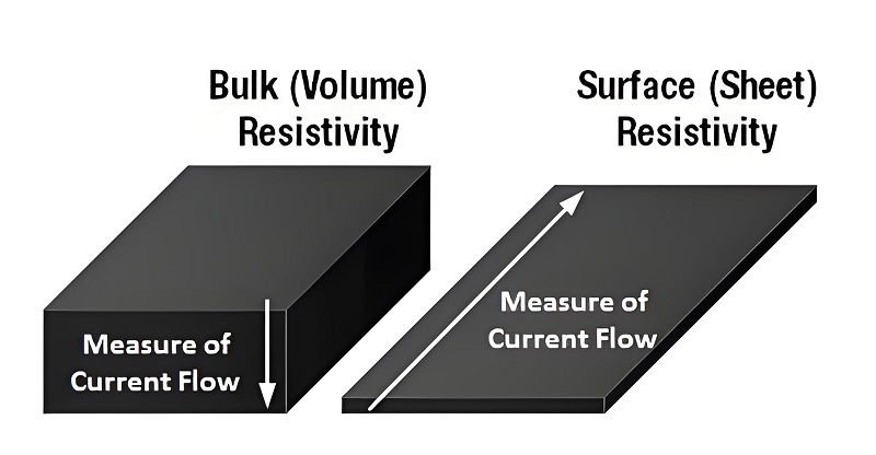
What is the Bulk Conductivity?

Bulk conductivity refers to the ability of a material to conduct electric current throughout its entire volume. This property is influenced by factors such as the material’s atomic structure and the presence of impurities. In simple terms, it measures how easily electrical charges can flow through the material when an electric field is applied. Copper, with its excellent bulk conductivity, is a top choice for electrical wiring and PCBs because of its efficiency in transmitting electrical signals.

What is the Conductivity of Copper?

Copper stands out due to its high electrical conductivity. The electrical conductivity of copper is about 5.8 × 10⁷ S/m, which is one of the highest of any metal. This makes it an ideal material for electrical wiring, connectors, and components in PCBs. Its high conductivity ensures that electrical signals travel with minimal resistance, enhancing the efficiency of devices.

This conductivity is essential when it comes to maintaining high-speed data transmission and power distribution. Copper’s low resistance reduces energy loss, ensuring devices run efficiently, which is why it’s so widely used in the electronics industry.

What is the Bulk Resistivity of Copper?

Bulk resistivity is essentially the inverse of conductivity and indicates how much a material resists the flow of electric current. Copper’s resistivity is very low—around 1.68 × 10⁻⁞ Ω·m, making it an excellent conductor. This low resistivity contributes to copper’s superior performance in applications that demand high-efficiency electricity flow, such as in the production of PCBs, which rely on copper’s excellent electrical properties.

In terms of practical applications, low resistivity allows copper to handle higher currents without excessive heat buildup, a critical factor in maintaining the reliability and longevity of electrical systems.

What is the High Electrical Conductivity of Copper?

The high electrical conductivity of copper is a key reason it’s used in almost all electrical wiring and devices. The structure of copper atoms allows for easy movement of free electrons, enabling efficient electrical current flow. This characteristic makes copper indispensable in applications where high efficiency and low loss are essential, such as in communication systems, automotive electronics, and renewable energy technology.

Furthermore, the high conductivity of copper ensures that devices and systems can operate at optimal efficiency without overheating. This makes it a preferred material for high-performance applications.

What is the Difference Between Conductivity and Resistivity?

While conductivity and resistivity are closely related, they describe two opposite properties. Conductivity measures a material’s ability to carry an electric current, while resistivity measures how strongly the material resists the flow of that current. The two are mathematically connected: high conductivity means low resistivity, and vice versa.

Understanding this difference is essential when designing electrical systems. For example, when choosing materials for PCBs, low resistivity (high conductivity) is vital for reducing energy loss and heat production, which ensures the system runs more efficiently and lasts longer.

What is the Role of Bulk Conductivity in Electrical Circuits?

The bulk conductivity of copper plays a crucial role in electrical circuits. In any circuit, especially complex ones like those found in PCBs, the conductivity of the materials used determines how easily electrical signals can travel from one point to another. Copper’s high bulk conductivity ensures that signals are transmitted quickly and with minimal interference.

Moreover, the efficiency of electrical systems is directly linked to conductivity. Poor conductivity materials result in energy loss and potential system overheating, which can reduce the lifespan of electronic devices. Copper’s role in maintaining high conductivity ensures that electronic devices perform at their best for longer periods.

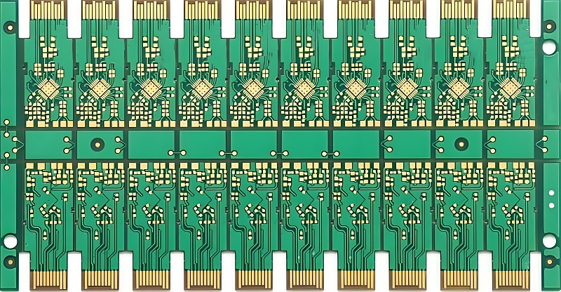
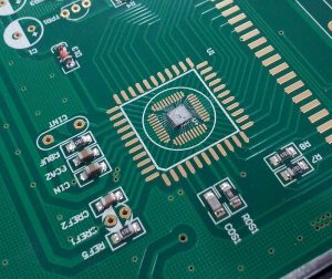
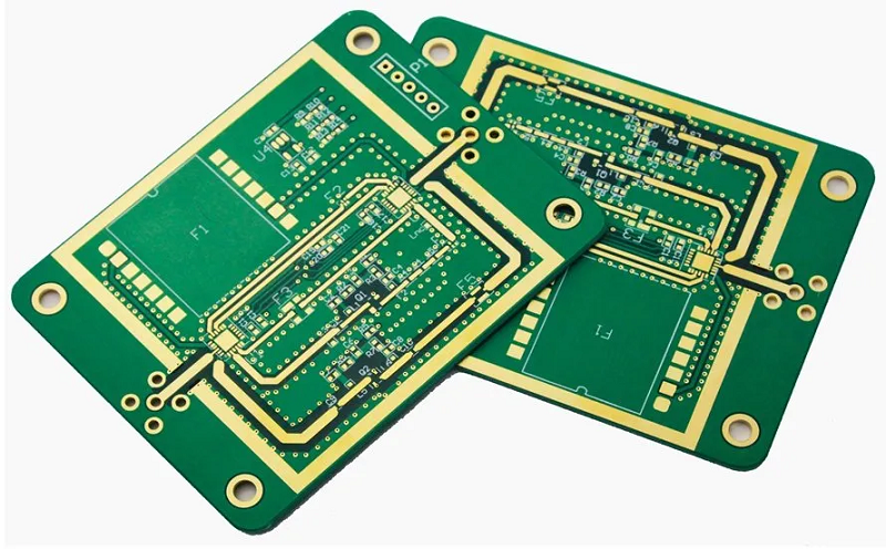
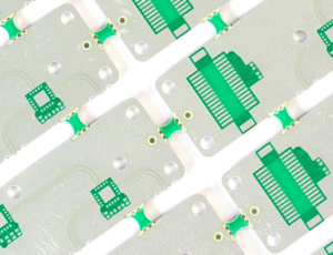
How Does Copper’s Bulk Conductivity Affect Its Use in PCBs?

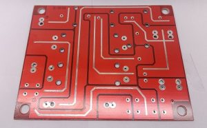
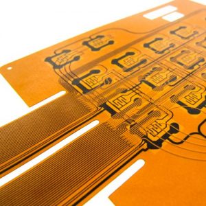
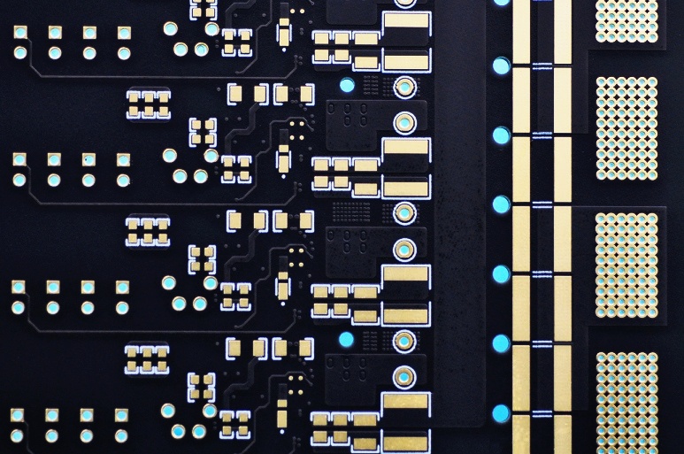
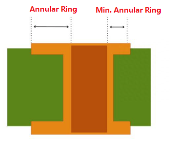
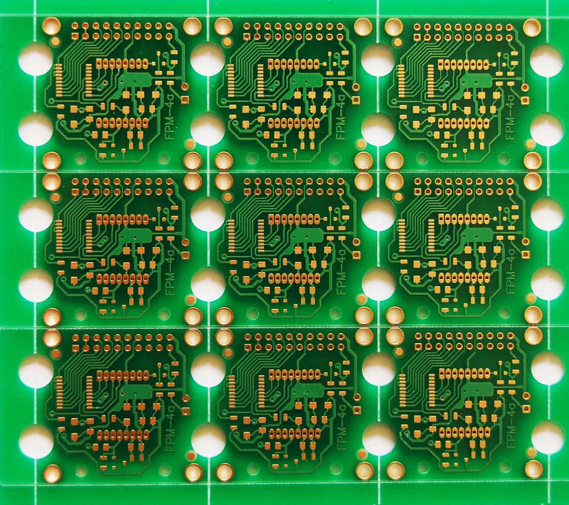
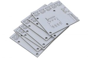
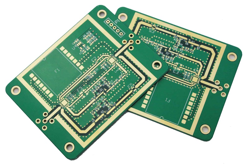
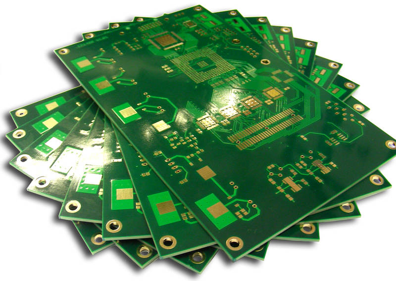
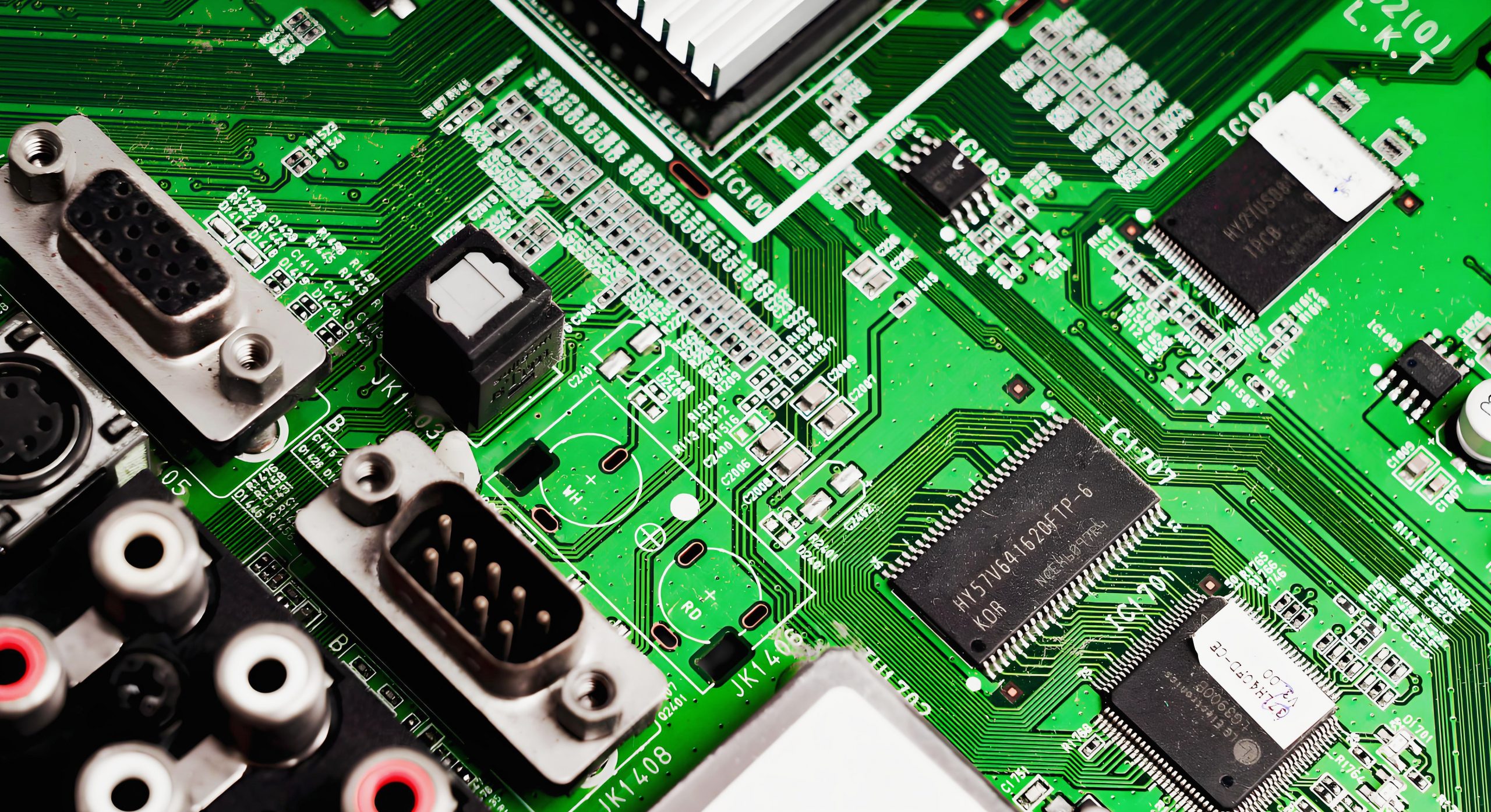
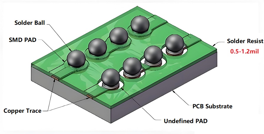
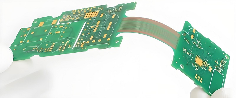
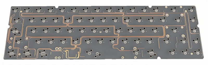
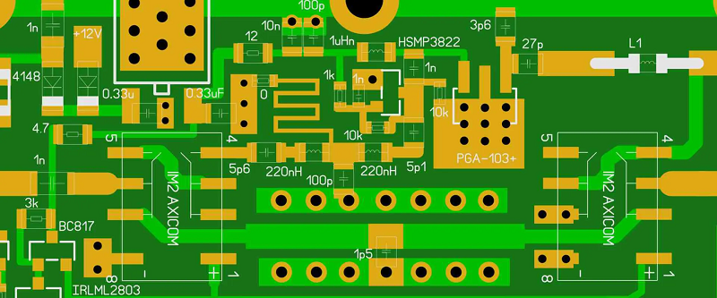
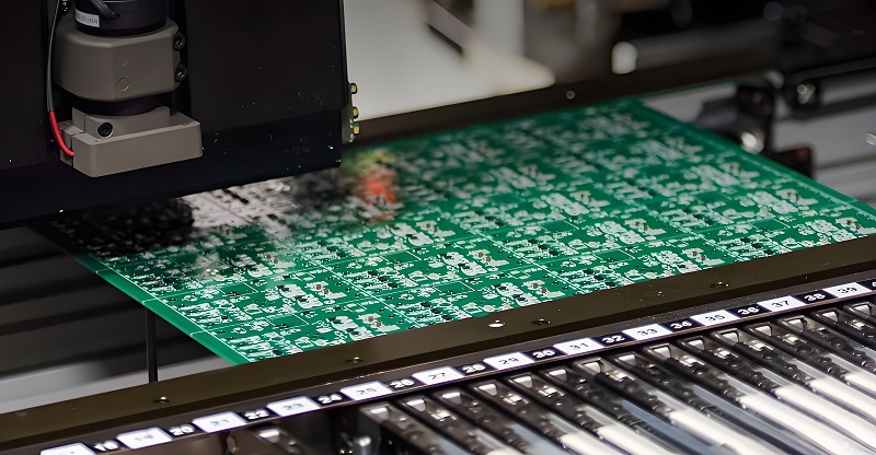
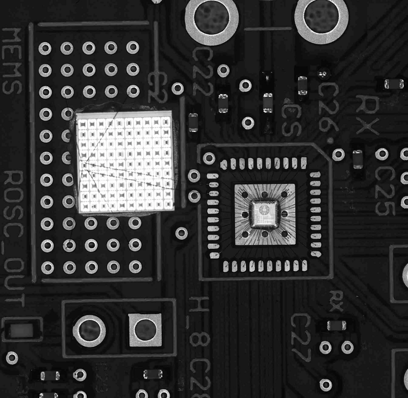
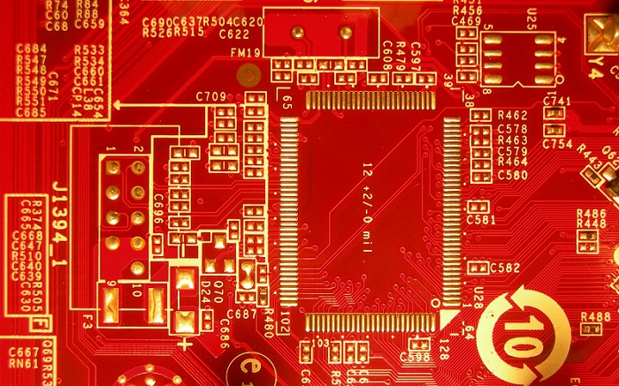
Copper’s bulk conductivity is particularly important in PCBs, as it ensures fast and efficient signal transmission. In PCBs, copper is used to create the traces that connect various components. These traces must have low resistance to avoid energy loss and signal degradation. The high conductivity of copper allows for thinner traces, which in turn makes PCBs more compact and cost-effective.

Additionally, copper’s excellent conductivity helps reduce the heat generated in PCBs, which is critical for preventing damage to sensitive components. This is especially crucial in high-performance electronics like processors and communication devices.

What Are the Key Factors Influencing the Bulk Conductivity of Copper?

Several factors influence the bulk conductivity of copper. Temperature is one of the most significant. As the temperature increases, the atoms in the copper vibrate more, which can hinder the movement of electrons and decrease conductivity. However, the electrical conductivity of copper increases with increase in temperature to a point. Beyond a certain threshold, the increase in resistance becomes more noticeable.

Another factor is the purity of the copper. Impurities in the copper can introduce obstacles to electron flow, reducing conductivity. High-purity copper, with minimal impurities, offers the best conductivity.

What Industries Benefit the Most from Copper’s High Bulk Conductivity?

Industries that rely on high-efficiency electrical systems benefit the most from copper’s high bulk conductivity. This includes the electronics industry, where copper is used in everything from circuit boards to microprocessors. The telecommunications sector also relies on copper for high-speed data transmission lines. Additionally, the automotive industry, particularly in electric vehicles, uses copper in wiring and batteries due to its excellent conductivity.

Moreover, industries involved in renewable energy, such as solar and wind power, use copper extensively. Copper’s high conductivity ensures that electrical systems in renewable energy applications are both efficient and durable.

In summary, the bulk conductivity of copper is a key factor in its widespread use across various industries. Its ability to efficiently conduct electricity makes it indispensable in electronics, telecommunications, automotive, and renewable energy sectors. Understanding the role of copper’s conductivity, and how it compares to other materials, can help businesses and engineers make informed decisions when designing electrical systems and devices. With its low resistivity and high conductivity, copper remains the material of choice for a wide range of applications, from power transmission to high-performance PCBs. At Best Technology, we specialize in high-quality, tailor-made PCBs, offering rapid delivery and unmatched customer support. Reach out to us at sales@bestpcbs.com for more information or questions.

You may also like

Annular Ring: What is Annular Ring PCB? How to Calculate it?
Thursday, February 20th, 2025

Annular rings are small but essential features form part of the vias, helping to create electrical connections between different layers of the PCB. In simple terms, the annular ring is the copper ring that surrounds the hole in a PCB, and its quality can determine the effectiveness of the entire board. If not designed or manufactured correctly, the annular ring can lead to issues such as unreliable connections, potential failure, or even defective PCBs. In this blog, you’ll learn the importance in PCB design and functionality, how to calculate it correctly to avoid common issues occurred during PCB manufacturing.

What is Annular Ring in PCB?

To understand the importance of the annular ring, let’s break down its role in a PCB. A PCB is composed of multiple layers, and the annular rings on a PCB are circular metal rings used for mounting components on the circuit board. Sometimes, it also called PAD. They serve as connection points for the leads of electronic components and are attached to the corresponding positions on the board via soldering or insertion.

Annular Ring: What is Annular Ring PCB? How to Calculate it?

The annular rings are typically made of copper or other conductive materials, forming a connection around the holes to ensure that electrical signals can pass from one layer to another. Without this copper ring, the via would lack the necessary conductive material to transmit electrical signals, leading to potential functionality and reliability issues.

PCB holes usually come in shapes such as circular, square, or oblong. Among these, the circular hole is the most common. These holes are used for mounting components, connecting wires between circuit layers, or linking pads across different layers. When designing a PCB, you can select the appropriate hole shape based on specific needs.

What is an Annular Ring in Physics?

While the concept of the annular ring in PCB manufacturing is straightforward, it’s also rooted in basic physics. In physics, an annular ring is a two-dimensional geometric shape characterized by an outer and inner radius, with the space between the two radii representing the actual “ring.” This geometric shape has applications in a variety of fields, from fluid dynamics to optics.

In the context of PCB design, the annular ring’s geometry ensures that there’s enough copper material around the hole to support electrical connections and mechanical integrity. Essentially, the annular ring in PCB design mirrors this physical concept, providing the necessary structure to allow electrical signals to flow reliably between layers.

What is the Function of an Annular Ring?

The primary function of an annular ring is circuit connection. The annular ring connects with other circuit layers or components via wires or pins, enabling the transmission and interaction of electrical signals. Without this ring, the via would not have any conductive material to establish the necessary connections, rendering it ineffective. Essentially, the annular ring is like a bridge that connects different parts of the PCB. In addition to this, there are some other functions that apply annular rings in a PCB:

Annular Ring: What is Annular Ring PCB? How to Calculate it?

1. Component Mounting

    The annular ring is used to secure and connect electronic components (such as integrated circuit chips (IC), diodes, resistors, etc.) to the PCB through their leads or solder balls.

    2. Soldering Connection

    The metal edge of the annular ring is used for soldering the leads or pads of electronic components, establishing a reliable electrical connection. Through soldering, a physical and electrical bond is created between the component and the PCB.

    3. Vias in Multi-Layer PCBs

    In multi-layer PCBs, the annular ring serves as a via, acting as a conductive channel that connects different circuit layers. Through these vias, signals, power, and ground lines can be transmitted between layers.

    What is the Difference Between Via and Annular Ring?

    While vias and annular rings often work in tandem, they are different components of a PCB.

    Via:

    • A via is a drilled hole in the PCB, gennerally <=0.5mm.
    • It is plated with copper to create an electrical pathway.
    • Vias provide vertical connectivity between PCB layers.
    • They act as the conduits for electrical signals across layers.

    Annular Ring:

    • An annular ring is the copper pad that surrounds the via.
    • It creates a stable landing zone for the via.
    • The annular ring enhances solderability and connection strength.
    • It also supports the mechanical integrity of the PCB.

    Key Differences:

    • A via is the actual hole that allows electrical passage; the annular ring is the copper area around that hole.
    • Vias serve as internal conductive channels, while annular rings ensure a robust link to the board’s traces.
    • Vias are created by drilling and plating; annular rings are defined during the PCB layout design.

    In essence, the via acts as a hole or passage for electrical signals, while the annular ring is the surrounding copper that ensures the electrical signals can flow reliably between the different layers of the PCB. Without the annular ring, the via would have no copper to connect it to the surrounding traces, compromising the integrity of the circuit board.

    How Do You Calculate the Annular Ring Size?

    The annular ring size is determined by the diameter of the via hole and the size of the copper pad around it. To calculate the annular ring size, you need to first measure the diameter of the via hole. Then, you need to determine the size of the copper pad around the hole, keeping in mind that the pad must be large enough to maintain a reliable connection. In general, there are outer annular ring size and inner annular ring size:

    Outer Annular Ring Size (OAR)

    • Calculate Format:

    Outer Annular Ring (OAR) = (Outer pad diameter – Plated hole diameter) / 2

    • Actual Case:

    Plated hole diameter = Finished hole diameter + 0.10mm (for all PTH) + 0.00mm (for all NPTH).

    • Example:

    For a copper pad thickness of 0.60mm and a finished hole diameter of 0.30mm (PTH), the calculation of the OAR is:

    OAR = [0.60mm – (0.30mm + 0.10mm)] / 2 = 0.10mm

    Annular Ring: What is Annular Ring PCB? How to Calculate it?

    Inner Annular Ring Size (IAR)

    • Calculate Format:

    Inner Annular Ring (IAR) = (Inner pad diameter – Electroplated hole diameter) / 2

    • Actual Case:

    Electroplated hole diameter = Finished hole diameter + 0.10mm (for all PTH) + 0.00mm (for all NPTH).

    • Example:

    For a 0.50mm copper pad and a 0.20mm finished hole diameter (PTH), the calculation of the IAR is:

    IAR = [0.50mm – (0.20mm + 0.10mm)] / 2 = 0.10mm

    Annular Ring: What is Annular Ring PCB? How to Calculate it?

    What is the Minimum Annular Ring Size on a PCB?

    The minimum annular ring (AR) on a PCB refers to the minimum amount of copper between the edge of the pad and the electroplated hole. The width of the minimum annular ring should be greater than or equal to the value defined in the PCB design.

    Annular Ring: What is Annular Ring PCB? How to Calculate it?

    When the annular ring is smaller than the specified width, the attachment of components may be affected, and there is a risk of pad cracking. In this case, the circuit may enter the pad, minimizing the current-carrying capacity of the circuit.

    Sometimes, the traces on the PCB need to connect to another layer. In such cases, the trace eventually passes through the pad. The via in the pad helps the trace move through and connect to another layer.

    Annular Ring: What is Annular Ring PCB? How to Calculate it?
    • t1: Minimum outer annular ring, on finished boards, must be >= 0.05mm.
    • t2: Minimum inner annular ring, on finished boards, must be >= 0.01mm.

    Common Annular Ring Issues During PCB Manufacturing

    Despite the importance of annular rings, issues can arise during the manufacturing process that impact their effectiveness. Some common problems include:

    • Undesired Annular Rings

    Undesired annular rings are a common issue that affects many designers when working with standard PCBs. If the pad size is too small, the PCB may not function properly because the hole takes up more space on the pad. To avoid this issue, making a prototype before mass production is necessary. Prototypes can prevent unnecessary annular rings from appearing before large-scale production of the circuit boards.

    • Missing Annular Ring

    A missing annular ring can occur if the design does not include an annular ring around the via, or if the annular ring was not correctly produced during manufacturing. This can lead to poor electrical connections, affecting the performance of the circuit.

    • Broken Annular Ring

    A broken annular ring occurs when drill tolerances cause the via to deviate from the center during manufacturing, leading to the annular ring breakout.

    Annular Ring: What is Annular Ring PCB? How to Calculate it?
    • Annular Ring Tangency

    Annular ring tangency refers to a situation where part of the via touches the edge of the pad, typically caused by the drill bit not being aligned with the markings. This can cause the via to deviate from the center and negatively affect the normal operation of the circuit.

    Annular Ring: What is Annular Ring PCB? How to Calculate it?

    What Can Best Technology Do for You?

    At Best Technology, we have over 18 years of experience in PCB manufacturing, and we understand the importance of the annular ring in creating reliable and high-quality PCBs. Our team of experts works closely with clients to ensure that every PCB is designed with the right annular ring specifications, minimizing the risk of defects and improving the overall performance of the circuit board. In additional to this, our sales-assistant will send EQ (engineer question) file and WF (working file for manufacturing) to customer for a final approval before starting production.

    We use state-of-the-art equipment and precision techniques to manufacture PCBs that meet the highest standards. Whether you’re designing a single-layer PCB or a complex multi-layer board, Best Technology has the expertise and experience to deliver high-quality PCBs that meet your needs. We’re here to support your projects and ensure that your PCBs are reliable, efficient, and built to last.

    Let us help you create the perfect PCB with the right annular ring design to ensure seamless electrical connections and superior functionality. Reach out to Best Technology today for your PCB needs!

    You may also like

    Thermal Conductivity of Copper: What is the K Value of Copper?
    Wednesday, February 19th, 2025

    Thermal conductivity of copper is one of the most important properties of the material, especially in industries like electronics and heat management. With its high thermal conductivity, copper plays a vital role in efficiently transferring heat, making it a go-to material for various applications, including Printed Circuit Boards (PCBs), heat sinks, and cooling systems. But what exactly is the K value of copper, and why should you care? Let’s dive into the fascinating world of copper’s thermal conductivity and how it impacts the way we use this versatile metal.

    What is the Thermal Conductivity of Copper?

    The thermal conductivity of copper is the measure of how well copper conducts heat. In simpler terms, it defines how easily heat flows through the material. The K value, or thermal conductivity, of copper is exceptionally high, approximately ranging from 380 to 401 W/(m·K), making it one of the most efficient materials for heat transfer. This characteristic is crucial in applications where efficient heat dissipation is required.

    The high thermal conductivity of copper means it can quickly absorb and release heat, which is why it’s widely used in applications such as wiring, heat exchangers, and cooling systems. This ability to efficiently manage heat is especially important in electronics and the manufacturing of PCBs.

    What Factors Affect the Thermal Conductivity of Copper?

    Several factors can influence the thermal conductivity of copper, and understanding them helps optimize copper’s use in various industries.

    Temperature: As temperature increases, copper’s thermal conductivity decreases slightly. However, copper still remains highly conductive compared to most other materials, even at higher temperatures. The temperature dependence of copper’s thermal conductivity is relatively low compared to some other materials.  

    Purity: Pure copper has the highest thermal conductivity. The thermal conductivity of pure copper is approximately 401 W/(m·K). Impurities or alloying elements in copper can reduce its ability to conduct heat. That’s why many applications rely on high-purity copper to ensure optimal thermal performance.

    Structure: The microstructure of copper also plays a significant role. For instance, copper that is in a crystalline form tends to have better thermal conductivity compared to non-crystalline forms.

    External Conditions: Environmental factors like pressure and surrounding gases can also affect how well copper conducts heat. In controlled environments, copper’s thermal conductivity can perform even better.

    What is the Thermal Conductivity of Stainless Steel Compared to Copper?

    When comparing copper to stainless steel, the difference in thermal conductivity is striking. Copper outperforms stainless steel by a significant margin. Taking 304 stainless steel as an example, its thermal conductivity is approximately 16 W/(m·K). This makes copper far more efficient at transferring heat, which is one of the reasons why copper is preferred for applications that require quick heat dissipation.

    While stainless steel has its own advantages, such as strength and corrosion resistance, its relatively low thermal conductivity means it’s not the best choice for applications that rely on fast heat transfer.

    What is the Most Thermally Conductive Metal?

    The most thermally conductive metal is actually silver, not copper. Silver has a thermal conductivity of around 429 W/m·K, which is slightly higher than copper. However, due to its cost and less common use, copper is generally preferred in industrial applications. Silver’s high thermal conductivity makes it ideal for specialized applications, but copper provides a more affordable solution without compromising performance in most heat management scenarios.

    Is Copper a Good Thermal Conductor?

    Absolutely! Copper is renowned for being one of the best thermal conductors. Copper is with High K value, it’s widely used in industries that require efficient heat transfer. Its ability to quickly dissipate heat makes it an excellent material for electronics, cooling systems, and heat exchangers.

    In fact, copper’s combination of high thermal conductivity, ductility, and strength makes it a popular choice for various industrial applications. It’s the material of choice when heat management is crucial, and it’s especially valued in the production of PCBs and other components in the electronics industry.

    Why is the Thermal Conductivity of Copper Important?

    The thermal conductivity of copper is essential because it directly affects the performance of the products that rely on copper for heat dissipation. Whether it’s in electronics, automotive systems, or home appliances, copper’s ability to efficiently transfer heat ensures that components remain within safe operating temperatures, preventing overheating and potential damage.

    For example, in PCB manufacturing, copper’s thermal conductivity is a critical factor in maintaining the performance and longevity of electronic devices. The better the heat dissipation, the longer the device can run without encountering thermal stress, which can lead to failures.

    How Does Copper Compare to Other Heat Sink Materials?

    Heat sinks are a crucial part of many electronic devices, and copper is often the material of choice for high-performance heat sinks. When compared to other materials, copper stands out due to its superior thermal conductivity. Aluminum, another popular heat sink material, is also effective but has a thermal conductivity of around 205 W/m·K to 237W/m·K—roughly half that of copper.

    This difference means copper heat sinks are better at transferring heat away from critical components, ensuring that electronics maintain optimal temperatures during operation. While aluminum is more affordable and lighter, copper’s superior thermal conductivity makes it the material of choice for applications where performance is critical.

    How Does Copper Thermal Conductivity Impact PCB Manufacturing?

    In PCB manufacturing, the thermal conductivity of copper is incredibly important. PCBs used in high-power applications, such as inverters and power supplies, rely on copper to effectively dissipate heat. A copper PCB has superior thermal management properties compared to other materials, ensuring that heat doesn’t build up and cause damage to sensitive components.

    Copper’s ability to transfer heat efficiently is one of the reasons it’s widely used in PCB designs. The material helps maintain a safe operating temperature, extending the lifespan of the board and preventing thermal-related failures. Additionally, copper’s high thermal conductivity is essential for ensuring that heat is evenly distributed across the PCB, preventing hot spots that can lead to malfunction.

    In many ways, the thermal conductivity of copper directly impacts the performance and reliability of electronic devices, making it a key factor in the PCB manufacturing process.

    The thermal conductivity of copper is a critical property that impacts many industries, particularly electronics and PCB manufacturing. Its high K value makes it an ideal material for heat management, ensuring that devices operate efficiently and remain within safe temperature ranges. Understanding copper’s thermal conductivity helps manufacturers optimize their designs for better performance, reliability, and longevity.

    As we’ve seen, copper is a good thermal conductor. Whether you’re designing PCBs, heat exchangers, or cooling systems, copper’s thermal conductivity is a key factor in ensuring your products perform at their best.

    At Best Technology, we specialize in producing high-quality PCBs that utilize copper’s outstanding thermal conductivity to deliver reliable, long-lasting solutions for your electronic needs. With over 18 years of experience, our expert team is ready to support your projects and provide the best thermal management solutions available. Warm welcome to reach us at sales@bestpcbs.com to get more information and personalized solutions.

    You may also like

    Mammoth 75 PCB Thickness: What Is The Standard PCB Thickness?
    Wednesday, February 19th, 2025

    The Mammoth 75 PCB thickness is a key factor that influences the overall feel, sound, and durability of your custom keyboard. Whether you’re building a new keyboard or upgrading your existing one, understanding the impact of PCB thickness is essential. In this blog, we’ll break down the ideal thickness for the Mammoth 75 PCB, explore the differences between various options, and help you make the right choice for your build.

    What is the Standard PCB Thickness?

    PCB thickness refers to the measurement of the circuit board’s overall depth. The 1.6 mm thickness is the most widely adopted standard across the electronics industry. This thickness provides an optimal balance of rigidity and durability, ensuring structural stability for most applications while remaining compatible with standard components and manufacturing processes.

    For mechanical keyboards, such as the Mammoth 75 PCB, 1.6 mm is frequently used as it offers sufficient rigidity to maintain switch alignment and resist flex during typing. However, some keyboards may use thinner PCBs (e.g., 1.2 mm) to introduce controlled flexibility, which can influence the typing feel or sound profile (e.g., in gasket-mounted designs). Conversely, thicker PCBs (e.g., 2.0 mm) are occasionally used to add weight or alter acoustics. Adjustments in thickness are typically made to optimize performance characteristics like sound, weight, or mechanical behavior, rather than aesthetics alone.

    What is the Difference Between 1.2 mm and 1.6 mm Keyboard PCB?

    When you compare a 1.2 mm PCB to a 1.6 mm PCB, the primary difference lies in rigidity and durability. A 1.6 mm PCB offers better structural support, making it more robust and resistant to bending or flexing during use. It also tends to provide a more solid feel, which many users prefer in their mechanical keyboards. On the other hand, 1.2 mm PCBs are lighter. They’re often chosen for keyboards that emphasize portability.

    The Mammoth 75 PCB thickness usually falls within the 1.6 mm category, ensuring a solid and sturdy feel, perfect for those who prioritize stability and a premium typing experience.

    How Thick Should a Keyboard PCB Be?

    The ideal Mammoth 75 PCB thickness depends on what you’re looking for in terms of typing experience and design goals. For most users, 1.6 mm is considered the sweet spot, as it balances durability with flexibility. A thicker PCB could result in a more rigid typing experience, but it may also add unnecessary weight. For those looking for a more flexible typing experience, a thinner PCB around 1.2 mm may be a better choice.

    When considering thickness, it’s important to also think about other components of the keyboard, such as the case material and plate. The PCB should complement these elements to create the ideal feel and sound profile.

    How Thick Should PCB Traces Be?

    PCB traces are the pathways that carry electrical signals across the board. The thickness of the traces plays a crucial role in the performance of the PCB. Typically, traces for mechanical keyboards are designed to handle current requirements without unnecessary width. For most Mammoth 75 PCB designs, trace thickness will typically be between 6 mils and 10 mils, depending on the current and signal requirements.

    In general, thinner traces can be used for low-power applications like key switches, while thicker traces are used where higher currents are involved. Ensuring that your PCB traces are appropriately sized is critical to ensuring reliable keyboard performance.

    What is the Mil Thickness of a PCB?

    The mil thickness of a PCB refers to its measurement in mils, where one mil equals one-thousandth of an inch. In custom mechanical keyboard builds, such as the Mammoth 75, the PCB thickness is often specified in mils to ensure it fits properly with the case and other components. For example, a typical Mammoth 75 PCB might be 1.6 mm (about 63 mil), but if you’re aiming for a more robust design, you may opt for a 2.4 mm (or 95 mil) thickness for additional durability and stability. Thicker PCBs offer greater durability and rigidity, contributing to a sturdier build that can better handle the stresses of long-term use.

    Does PCB Thickness Matter?

    Yes, PCB thickness absolutely matters when it comes to building a custom mechanical keyboard like the Mammoth 75. The thickness of the PCB can influence several factors, including:

    Weight and feel: Thicker PCBs provide a more solid, premium feel.

    Sound profile: Thicker PCBs can dampen vibrations slightly, contributing to a deeper or more muted sound. Thinner PCBs may allow more resonance, potentially brightening the acoustics. However, sound is more heavily influenced by plate material, mounting style, and case design.

    Durability: A thicker PCB will usually be more durable and resistant to warping over time.

    In summary, choosing the right Mammoth 75 PCB thickness can significantly enhance the typing experience, depending on personal preference and design goals.

    Are All Keyboard PCBs the Same?

    No, all keyboard PCBs are not the same. They come in various shapes, sizes, materials, and thicknesses. The Mammoth 75 PCB is specifically designed for a 75% layout, which influences its size and port placement. Additionally, the choice of material, like FR4, affects the PCB’s durability and weight.

    When choosing a PCB for your custom build, it’s essential to ensure that it matches your keyboard case and plate. Not all layouts and sizes will fit, so it’s crucial to pick a PCB that works well with the other components.

    In conclusion, understanding Mammoth 75 PCB thickness is essential for anyone looking to build or modify a custom mechanical keyboard. The thickness of the PCB affects everything from durability and sound to the overall typing experience. While 1.6 mm is the most common thickness for high-quality keyboards, some users may prefer a thinner or thicker option based on their specific needs.

    By knowing the differences in thickness, trace size, and material, you can choose the right PCB thickness for your keyboard. Whether you’re designing your dream Mammoth 75 keyboard or just curious about PCBs, the thickness plays a pivotal role in shaping your keyboard’s performance and feel. Best Technology excels in delivering customized, premium PCB solutions with fast turnaround times, supported by exceptional customer service. For details or inquiries, feel free to contact us at sales@bestpcbs.com.

    You may also like

    What is Solder Resist? Solder Resist Material
    Wednesday, February 19th, 2025

    Solder resist is a key material used in PCB (Printed Circuit Board) manufacturing to protect the circuit traces. This thin layer, typically green in color, ensures that solder only adheres to specific areas during the assembly process. Without solder resist, PCBs could suffer from short circuits, poor connections, and overall performance issues.

    What is Solder Resist? Solder Resist Material

    What is a Solder Resist?

    Solder resist, sometimes known as a solder mask, is a protective layer applied to the surface of a PCB. In essence, solder resist is an insulation ink, its primary function is to prevent the solder from flowing onto unwanted areas during the soldering process. By applying a layer of solder resist, manufacturers can ensure the quality and reliability of the board’s electrical connections.

    The solder resist material protects the copper traces, ensuring that the PCB functions correctly by providing an insulated surface. It also enhances the overall durability of the PCB by preventing oxidation or damage to the copper.

    Types of Solder Resist

    There are several types of solder resist materials, each offering different benefits for specific manufacturing processes. Each type of solder resist serves its purpose based on the complexity of the PCB design and the manufacturing process involved. The most commonly used solder resist types are:

    • Liquid Solder Resist: Applied using a spray or traditional screen printing method, this type is the most popular and offers ease of application. In generally, it is a default types of soler resist if there are no any special requirements from customers.  
    • Dry Film Solder Resist: This is a laminated material that is applied to the board before exposure to ultraviolet (UV) light. After exposure, the unwanted parts of the resist are washed away.
    • Photo-sensitive Solder Resist: It is a special variant that reacts to UV light, making it ideal for highly detailed, small-scale PCB designs.
    Types of Solder Resist

    Photos of Solder Resist

    While solder resist is typically green, variations exist depending on the design and function of the PCB. Photosensitive solder resist, for example, is often used in more intricate PCB designs because it allows for precise control of where the resist material is applied. Below are some examples of PCBs showcasing different types of solder resist and their impact on the circuit layout.

    What Does Solder Resist Do?

    Solder resist plays several critical roles in PCB manufacturing:

    1. Prevents Short Circuits

    One of the key roles of solder resist is to prevent solder from adhering to areas other than the intended electrical contacts on a printed circuit board (PCB). During the soldering process, it ensures that solder only sticks to the pads where components are placed.  By blocking solder from unwanted areas, it ensures that electrical connections are not unintentionally bridged.

    2. Protecting Circuit Patterns from Dust, Heat, and Moisture

    Solder resist acts as a protective shield, safeguarding the delicate circuit patterns from external factors like dust, heat, and moisture. These environmental conditions can otherwise compromise the performance and longevity of the PCB.

    3. Supports Manufacturing / Smooth Manufacturing Process

    A layer of solder resist guides the soldering process by clearly defining where the solder should go, smooth the whole process, making the entire assembly process more efficient.

    What Does Solder Resist Do?

    4. Maintaining Electrical Insulation Between Circuit Patterns

    As electronic devices become smaller and more complex, the circuit patterns on PCBs have shrunk significantly, 50 to 150 ”m dimensions are always commonly used in the market. And even thinner on advanced package boards. Solder resist ensures that these circuit patterns remain electrically insulated from one another, preventing accidental short circuits.

    Solder Resist Material

    Solder resist materials vary based on the requirements of the PCB and the intended application. The most common materials used include:

    • Epoxy-based resists: These are widely used due to their excellent adhesion and resistance to high temperatures and chemicals.
    • Acrylic-based resists: Known for their fast curing times and easier handling, they are suitable for mass production.
    • Polyimide-based resists: Used for high-performance applications, especially in extreme environments.

    The material selected depends on factors such as the desired performance, operating environment, and manufacturing capabilities. Each material has its advantages and is chosen according to the specific requirements of the PCB design.

    What is the Thickness of Solder Resist?

    The thickness of solder resist plays an important role in the overall performance of the PCB. Typically, the solder resist layer has a thickness between 15 and 30 microns (0.5mil to 1.2mil). The solder mask tends to be thinner near the edges of the traces and can be as thin as 0.3 mils or even less.

    What is the Thickness of Solder Resist?

    Typically, it’s recommended to have around 0.5 mils of solder mask covering the traces. This thickness ensures optimal protection without interfering with the soldering process or compromising the performance of the circuit. The exact thickness may vary depending on the complexity of the PCB design, but in general, it is thick enough to protect the copper traces while being thin enough to not interfere with the components’ performance. If you can’t make a decision about the solder resist thickness, it is a good way to ask a trust PCB manufacturer to get your answer, such as Best Technology.

    Solder Resist vs. Solder Mask

    Many people are confused about solder mask and solder resist: “Are they same or what are the differences between them?”

    Actually, the terms solder resist and solder mask are essentially referring to the same concept. Both terms describe the protective layer applied to PCBs to prevent solder from bridging unwanted areas. While “solder mask” is commonly used, “solder resist” is more technically accurate since the resist material resists the solder during the assembly process. However, both terms are widely interchangeable in the industry.

    Solder Resist Colors

    While green is the most widely recognized color for solder resist, it’s far from the only option available. Solder resist can be found in a variety of colors, including red, blue, black, yellow, and even white, depending on the requirements of the PCB design or the specific application where this PCB will be used. These color variations serve different purposes, ranging from aesthetic preferences to functional considerations.

    For example, some high-end or custom-designed PCBs may use colors like black or blue to create a distinct visual identity or to align with branding guidelines. In industries like aerospace or medical devices, where high-performance and unique design are often crucial, color may also be chosen for its visibility during the manufacturing process or in final product assembly.

    However, the color choice isn’t only about appearance. In some cases, it can help with thermal conductivity, which can be important for applications that involve high-power circuits. Additionally, certain colors are more reflective under UV light, which aids in the photolithographic process. For example, blue solder resist can be beneficial for high-resolution applications, as it tends to make the ultraviolet light exposure process more precise. We’ve introduced the detailed functions about PCB colors in our other blogs:

    Why is Solder Resist Green?

    While various colors of solder resist exist, green has become the industry standard for a variety of reasons, many of which are practical rather than just aesthetic.

    Why is Solder Resist Green?
    • High Contrast and Visibility

    One of the main reasons for the green color’s dominance is its high visibility, especially under ultraviolet (UV) light. During the PCB manufacturing process, photolithography is used to expose specific areas of the board to UV light. Green solder resist is highly visible under UV, so FQC (final quality check) inspectors can inspect the board for defects or imperfections in the soldering process.

    • Optimal Performance in Photolithography

    The process of applying solder resist involves exposing the board to UV light, which causes the resist material to harden in specific patterns. Green solder resist material is particularly well-suited to this process, as it is engineered to react efficiently to UV exposure.

    • Cost-Effectiveness and Standardization

    Another reason green solder resist is so commonly used is its cost-effectiveness. Green has become the default color because it is the most widely produced, and cost effective. Standardizing on green also simplifies production processes, as manufacturers can keep a consistent stock of the same type of material.

    • Historical Tradition

    The history of green solder resist dates back to the early days of PCB manufacturing. Green was originally chosen due to its availability, as it was one of the first colors of solder resist to be mass-produced. Over time, this color became synonymous with PCBs, and manufacturers continued to use it because it had already proven reliable and effective.

    • Visual Appeal

    Finally, there’s a practical and visual appeal to the green color. Green provides a clean, professional look for most PCBs and offers a neutral backdrop that allows the components and circuitry to stand out clearly. This is important, especially for high-precision and high-performance boards that need to be easily inspected for quality.

    At Best Technology, we pride ourselves on over 18 years of expertise in the PCB manufacturing industry. As a trusted leader, we specialize in providing high-quality, reliable PCBs tailored to meet the specific needs of a wide range of industries, including automotive, telecommunications, and consumer electronics. Our expertise in solder resist application plays a vital role in maintaining the integrity of your circuits and preventing soldering issues while enhancing the overall lifespan of your PCBs. Meanwhile, we offer various color of solder resist, whatever you want, we can make it into reality. Contact us and get your own customized PCB now!

    You may also like

    Non-Flex Cut vs Flex Cut PCB: What Is Flex Cut PCB?
    Tuesday, February 18th, 2025

    The debate of non-flex cut vs flex cut PCB has been a common topic for engineers and manufacturers. When designing printed circuit boards (PCBs), one key decision is whether to use a flex cut or non-flex cut PCB. These two types of PCBs serve different purposes, with unique advantages depending on the application. But how do they differ, and when should you use each? This guide will dive into the specifics, providing you with insights to make an informed decision.

    What is a Flex Cut PCB?

    A flex cut PCB is a type of printed circuit board that’s designed to be flexible. Unlike traditional rigid PCBs, flex PCBs can bend and flex without compromising the performance of the electrical circuits. This flexibility is achieved by using materials such as polyimide, which allows the board to conform to various shapes and spaces.

    Flex cut PCBs are commonly used in devices where space is limited or for designs that require a dynamic or compact setup, such as in wearable tech or mobile phones. Their flexible nature provides the freedom to design intricate layouts without being restricted by rigid geometries.

    What is the Difference Between Flex Cut and Non-Flex Cut PCB?

    The main difference between flex cut and non-flex cut PCBs lies in their physical structure and flexibility. As mentioned, flex cut PCBs are made from flexible materials, which means they can be bent, twisted, or folded. This flexibility makes them suitable for applications where space constraints are a concern, and the board needs to fit into non-traditional forms or be more compact.

    In contrast, non-flex cut PCBs, often referred to as rigid PCBs, are built using rigid substrates like FR4 or aluminum, providing stability and durability. These boards do not bend and are generally used in devices that do not require flexibility.

    Both types of PCBs have their unique advantages. Flex cut PCBs are best for space-saving and adaptability, while non-flex cut PCBs are ideal for products that need more stability and rigidity.

    Why Use a Flex PCB?

    There are several reasons to opt for a flex PCB in certain applications. One of the biggest advantages is its ability to save space. Flex PCBs can be folded or shaped to fit into areas where rigid PCBs cannot. This makes them an excellent choice for compact electronic devices such as smartphones, cameras, and medical equipment.

    Additionally, the flexibility allows for more robust designs in environments with high mechanical stress, such as robotics or wearables. Flex PCBs can withstand vibration and movement better than rigid boards, offering better durability in these conditions.

    Finally, the lightweight nature of flex PCBs contributes to the overall efficiency of the product, making them an essential component in modern, miniaturized electronics.

    What is an FR4 Plate?

    FR4 is a widely used material in the manufacturing of rigid PCBs. It stands for “Flame Retardant 4” and is a type of fiberglass epoxy laminate. The FR4 material provides excellent strength, low moisture absorption, and good electrical insulation properties.

    While FR4 is typically used for non-flex cut PCBs, it can also be used in multi-layer flexible PCBs in certain designs. Its role is to provide stability and electrical insulation, making it a crucial material in traditional PCBs.

    What is Tri-Mode Non-Flex Cut Hotswap PCB?

    Tri-mode non-flex cut hotswap PCBs are a specialized type of PCB designed for mechanical keyboards, offering a flexible, user-friendly experience. The term “tri-mode” refers to the ability to support multiple connection types, such as wired, Bluetooth, and wireless.

    The non-flex cut hotswap design enables users to easily replace or swap out switches on the keyboard without the need for soldering. This makes it ideal for enthusiasts who want to customize their keyboards with different types of switches. It combines the advantages of non-flex cut rigidity with the versatility of hotswapping.

    What is a Rigid-Flex PCB?

    A rigid-flex PCB is a hybrid of both rigid and flexible PCB technologies. It consists of both rigid and flexible sections integrated into a single board. These PCBs offer the best of both worlds, combining the stability and reliability of rigid PCBs with the flexibility of flex PCBs.

    Rigid-flex PCBs are often used in high-performance applications such as aerospace, medical devices, and automotive systems. They provide a compact solution where multiple PCB types need to coexist, and their flexible sections can be bent or folded to fit complex spaces.

    What Are the Disadvantages of Rigid-Flex PCBs?

    Despite their advantages, rigid-flex PCBs come with some drawbacks. One major disadvantage is their cost. Due to the complexity of manufacturing, rigid-flex PCBs tend to be more expensive than traditional rigid or flex PCBs.

    Additionally, the design and production process for rigid-flex PCBs is more intricate, requiring higher precision and more time. This can also lead to longer lead times for production, which may not always be ideal for projects with tight deadlines.

    When Should I Use a Flex PCB?

    Flex PCBs are perfect for applications where flexibility, compact design, and space-saving are important. You should use a flex PCB when your product needs to fit into tight or unique spaces, like wearable devices, medical equipment, or consumer electronics.

    They are also a good choice for products that need to endure repetitive movement or vibrations. In situations where the PCB needs to be bent or folded without breaking, such as in robotics or automotive designs, flex PCBs offer exceptional reliability.

    Are Flexible PCBs More Expensive?

    Flexible PCBs generally come at a higher cost compared to non-flex cut PCBs. This is due to the specialized materials and the intricate manufacturing process required for flexible designs.

    However, despite the initial cost increase, flex PCBs can provide long-term cost savings by reducing the overall size of the device and minimizing the need for additional components or connectors. For applications where space is crucial or where traditional PCB designs would be too bulky, the investment in a flex PCB can pay off in the long run.

    In the debate of non-flex cut vs flex cut PCB, the right choice ultimately depends on the needs of your project. Flex PCBs excel in compactness and flexibility, making them a great choice for dynamic, space-constrained designs. On the other hand, non-flex cut PCBs offer superior stability and durability for applications where rigidity is key.

    For some projects, you might even find that combining the benefits of both technologies, like in rigid-flex PCBs, offers the perfect balance of performance and flexibility. When making your decision, consider the design requirements, budget, and long-term needs of your application.

    By understanding the differences between flex and non-flex cut PCBs, you can make the best choice for your next project, ensuring efficiency, durability, and performance. Best Technology sets itself apart by providing top-notch, customized Non-Flex Cut and Flex Cut PCB products, quick delivery, and superior customer care. Contact us at sales@bestpcbs.com for inquiries or further details.

    You may also like

    1.6t vs 1.2 PCB: Why are PCBs 1.6 mm thick?
    Tuesday, February 18th, 2025

    The debate between 1.6t vs 1.2 PCB is a common one for those designing or customizing mechanical keyboards. The thickness of a PCB affects not only the overall durability but also the typing experience. Whether you prioritize a solid feel with a 1.6 mm PCB or prefer the lighter, more flexible nature of a 1.2 mm PCB, understanding these differences can help you make the right choice. In this blog, we’ll break down the key distinctions, and show you how the thickness of your PCB can influence the performance and comfort of your keyboard.

    What is the difference between 1.2 and 1.6 PCB?

    The primary difference between a 1.2 PCB and a 1.6 PCB is the thickness of the board itself. A 1.2 PCB is 1.2 millimeters thick, while a 1.6 PCB measures 1.6 millimeters. The thickness of a PCB impacts its durability, rigidity, and overall feel in applications such as mechanical keyboards.

    A 1.2 mm PCB is often used in keyboards that require a more flexible, lighter feel. It’s commonly chosen for lightweight builds or when aiming for a slim profile. On the other hand, a 1.6 mm PCB is thicker, providing greater rigidity, which results in a more solid, firm keypress experience. This thickness is favored in high-end mechanical keyboards, where stability and a more premium feel are prioritized.

    Why are PCBs 1.6 mm thick?

    PCBs are typically 1.6 mm thick because this thickness offers an excellent balance between durability and flexibility for most applications. At 1.6 mm, the board is sturdy enough to support complex circuit designs and ensure reliable performance, yet it remains thin enough to fit comfortably within most electronic devices, including keyboards.

    The 1.6 mm thickness is the industry standard for many consumer electronics, as it can accommodate a variety of components without compromising the integrity of the circuit. It’s also an ideal thickness for creating a uniform look in keyboards, ensuring that all components fit together neatly while still maintaining high-quality performance.

    What is the thickness tolerance of a 1.6 mm PCB?

    The thickness tolerance of a 1.6 mm PCB generally falls within a range of ±0.1 mm. This means that the actual thickness of the PCB can vary slightly, typically between 1.5 mm and 1.7 mm, depending on the manufacturing process. Tolerance is an important factor because even slight variations in thickness can affect the fitting and performance of components, especially in high-precision builds like mechanical keyboards.

    However, manufacturers ensure that the tolerance level is within an acceptable range to prevent any significant issues when assembling the keyboard. This makes it easier to work with PCBs of this thickness, as the components are more likely to fit correctly and perform optimally.

    What is the most common PCB thickness?

    The most common PCB thickness is 1.6 mm, particularly for consumer electronics, including keyboards, smartphones, and other portable devices. This thickness strikes the perfect balance between strength and flexibility, making it the default choice for many applications. Whether you are designing a simple circuit or a more advanced mechanical keyboard, the 1.6 mm PCB provides the reliability and durability needed for long-term use.

    In keyboards, this thickness is widely used for both standard and custom builds. It’s not too thin to compromise the keyboard’s structure, and it’s not so thick that it adds unnecessary bulk.

    What is the minimum thickness of a PCB?

    The minimum thickness of a PCB depends on several factors, including the materials used, the intended application, and the manufacturing process. Typically, the thinnest PCB available is around 0.2 mm, though PCBs thinner than this can become fragile and less durable.

    For practical applications like keyboards, it’s rare to see PCBs thinner than 1.2 mm, as they may struggle to support the components required for stable keypresses. A thinner PCB can result in a less solid typing experience, which is why manufacturers typically avoid using extremely thin PCBs for high-performance builds.

    What is the thinnest PCB material?

    The thinnest PCB materials are typically made from flexible substrates, such as polyimide or polyester films. These materials allow for extremely thin designs that can be as low as 0.2 mm. These ultra-thin PCBs are often used in applications where space is limited, such as in wearable electronics or medical devices.

    However, it’s important to note that these thin materials often sacrifice some rigidity and may not be suitable for all types of keyboards. While they work well for compact or flexible designs, a more rigid PCB like the 1.2 mm or 1.6 mm versions is usually preferred in mechanical keyboards for their stability and performance.

    Does PCB thickness matter?

    Yes, PCB thickness does matter, especially when designing keyboards or other precision electronics. The thickness of the PCB affects the overall rigidity, weight, and feel of the final product. In a keyboard, for example, a thicker PCB (like the 1.6 mm version) will create a sturdier, more solid feel with less flex during typing.

    Thicker PCBs are often preferred in mechanical keyboards because they provide a more premium typing experience and reduce the likelihood of issues such as warping or bending. On the other hand, thinner PCBs (such as the 1.2 mm version) offer a lighter and more flexible feel, making them suitable for custom builds or portable devices where weight and space are critical considerations.

    Are PCB switches hot swappable?

    Hot-swappable PCB switches allow users to change switches without soldering. Many mechanical keyboards now feature hot-swappable PCBs, providing the flexibility to try different switches or replace worn-out ones with ease.

    However, not all PCBs are hot-swappable. A PCB must be designed specifically with hot-swapping functionality in mind, meaning that the PCB must have switch sockets and a proper electrical layout to support this feature. Many high-end 1.6 mm PCBs include this option, while thinner or cheaper PCBs might not.

    In summary, the choice between 1.6t vs 1.2 PCB comes down to the specific needs of your project. While the 1.6 mm PCB offers greater rigidity and durability, the 1.2 mm PCB provides a lighter and more flexible option. For keyboards, both thicknesses have their merits, depending on whether you’re looking for a more solid typing experience or a sleeker, more portable design.

    When selecting a PCB thickness, it’s essential to consider not only the thickness itself but also the application and overall design goals. Whether you’re building a custom keyboard or upgrading an existing one, understanding these PCB variations will ensure that you choose the right components for your needs.

    By opting for the right PCB thickness and features like hot-swappable switches, you can enhance your keyboard’s functionality and enjoy a superior typing experience. We offer a full range of PCB products in small quantities, ensuring fast delivery and the highest quality standards at Best Technology. Reach out to us at sales@bestpcbs.com for more information or questions.

    You may also like

    Board Printed Circuit: What Is The Printed Circuit Board?
    Friday, February 14th, 2025

    A board printed circuit (PCB) is the heart of almost every electronic device, acting as the foundation that connects various components to create functional circuits. Whether you’re using a smartphone, a computer, or even a household appliance, chances are there’s a PCB working behind the scenes to ensure everything runs smoothly. As technology continues to evolve, so do the designs and capabilities of PCBs, making them more efficient, reliable, and versatile. In this guide, we will explore the essential aspects of PCBs, from their design and cleaning methods to testing and understanding their purpose.

    What Is PCB in Electronics?

    A board printed circuit, commonly known as a PCB, is an essential component in almost every electronic device. It serves as a platform where different electronic components, such as resistors, capacitors, and microchips, are connected to form a circuit. The board is typically made from a non-conductive material, with copper traces etched onto its surface to provide pathways for electricity. This structure allows for compact, reliable, and efficient designs in everything from smartphones to computers.

    In essence, PCBs play a pivotal role in modern electronics. They not only ensure proper electrical connections but also provide mechanical support to various components. The design and manufacturing of PCBs have evolved significantly, resulting in numerous types and designs tailored for specific needs.

    Is It PWB or PCB?

    You may have heard the term PWB, or Printed Wiring Board, used interchangeably with PCB. Both terms refer to the same thing, but they are often used in different contexts. PWB refers more to the wiring aspect of the board, highlighting the copper traces used for electrical connections. On the other hand, PCB is a broader term that encompasses the entire board, including its physical structure and additional features such as layers, vias, and components.

    The term PCB is generally more common in the industry, as it reflects the comprehensive role the board plays in the overall functionality of an electronic device.

    What Is the Purpose of a PCB?

    The primary purpose of a printed circuit board is to electrically connect and mechanically support electronic components. By providing a compact and organized layout for components, PCBs help reduce the complexity of wiring and improve reliability. In high-speed circuits, such as those used in communication systems, the PCB ensures that signals are transmitted efficiently.

    Additionally, PCBs serve to protect components from environmental factors such as moisture and dust. They also contribute to heat dissipation by directing thermal energy away from sensitive components. With the evolution of technology, PCBs have become more specialized, designed to handle high-frequency signals, support multi-layer configurations, and integrate various types of components.

    How to Clean Printed Circuit Boards?

    Cleaning printed circuit boards (PCBs) is a crucial step in maintaining the integrity and longevity of electronic devices. Dust, grime, and flux residues can accumulate on the surface of the board over time, potentially causing performance issues or short circuits.

    To clean a PCB, you can use isopropyl alcohol and a soft brush. Gently scrub the surface of the board, avoiding excessive pressure to prevent damaging delicate components. After cleaning, ensure the board is completely dry before reassembling the device. If there are any visible traces of flux or solder, they can be cleaned with a specialized flux remover.

    In some cases, you may need to use a more thorough cleaning process, such as ultrasonic cleaning, especially for boards with complex structures or densely packed components.

    How to Connect Multiple PCBs Together?

    In many modern electronics, it is common to have multiple PCBs working together to perform different functions. These PCBs can be connected through various methods, depending on the complexity and requirements of the design.

    One common method is using connectors that link multiple PCBs together, allowing them to communicate with each other. For example, ribbon cables or flexible flat cables (FFCs) can be used for this purpose, providing a compact and reliable connection.

    Alternatively, PCBs can be connected using solder bridges or by mounting them on the same chassis. In advanced designs, flexible PCBs can be used to interconnect different sections of a device, ensuring flexibility and reducing the need for rigid connectors.

    Why Are Circuit Boards Green?

    You might have noticed that most circuit boards, including printed circuit boards, are green. This is due to the use of a green solder mask, which covers the copper traces and protects them from oxidation and damage. The green color is a result of the specific chemicals used in the solder mask. While green is the most common color, PCBs can also be manufactured in other colors like red, blue, or black. The color itself is more about aesthetic preference or company branding than functionality.

    The solder mask not only provides a protective barrier but also improves the board’s durability and resistance to harsh environments. The green color, in particular, is chosen because it provides high contrast with the copper traces, making it easier to inspect the board visually.

    What Is Printed Circuit Board Used For?

    Printed circuit boards are used in virtually all modern electronics. They form the backbone of devices such as smartphones, televisions, computers, and medical equipment. Their versatility makes them indispensable in a wide range of industries, from telecommunications to automotive applications.

    In consumer electronics, PCBs connect components like microprocessors, memory modules, and power supply units, enabling the device to function as intended. In more specialized applications, such as aerospace or automotive industries, PCBs are designed to meet strict requirements for reliability and performance under extreme conditions.

    Additionally, PCBs play an important role in emerging technologies like 3D printing and wearables. For example, the development of 3D printed circuit boards allows for more intricate designs and faster prototyping, which can lead to innovative new products.

    How to Test a Printed Circuit Board?

    Testing a printed circuit board is an essential step in ensuring the functionality and reliability of a device. There are several methods for testing PCBs, depending on the complexity of the design and the required standards.

    The simplest form of testing is a visual inspection, where the board is examined for physical defects such as broken traces, misaligned components, or solder bridges. This is often followed by electrical testing, where the board is powered up, and various signals are checked to ensure proper operation.

    In more advanced applications, automated optical inspection (AOI) and X-ray inspection are used to detect issues that are not visible to the naked eye. For high-frequency circuits, specialized tools such as oscilloscopes and spectrum analyzers are used to verify signal integrity.

    In summary, a printed circuit board (PCB) is more than just a platform for connecting electronic components—it is the foundation of modern electronics. From its role in providing electrical connections to its contribution to device durability, PCBs are essential in virtually every electronic product we use today. Whether you’re designing a simple circuit or developing a complex device, understanding PCB manufacturing, testing, and cleaning is crucial.

    At Best Technology, we are committed to providing high-quality PCBs tailored to your needs. With years of expertise in PCB manufacturing, we deliver products that meet the highest industry standards. Get in touch with us at sales@bestpcbs.com for any questions or additional information.

    You may also like

    Chip On Board (COB)? Discover Its Benefits in LED Technology
    Wednesday, February 12th, 2025

    Chip On Board (COB) technology is transforming the way we approach lighting and electronics by offering higher efficiency, compactness, and enhanced performance. In today’s rapidly evolving world of LEDs and high-performance displays, COB has become a game-changer. Whether you’re looking for brighter, more energy-efficient lighting solutions or advanced electronic designs, COB delivers superior results. This article will explore what COB is, how it works, its advantages, and why it’s becoming the go-to solution for many industries. Let’s dive deeper into how Chip On Board technology is revolutionizing the world of LEDs and beyond.

    What Does Chip On Board Mean?

    Chip On Board (COB) is a technology that involves mounting bare semiconductor chips directly onto a circuit board. The chips are typically used for LED applications, where they’re attached to the board without the use of traditional packaging methods. In simpler terms, instead of using individual LED packages, COB technology allows for the integration of multiple LEDs into a single unit, which increases performance and reduces space.

    This innovative approach makes the board more efficient in transferring heat and enhances the overall durability of the light source. Over time, COB has become a popular choice in high-performance lighting and electronic systems due to its compact nature and increased energy efficiency.

    What is a Chip-on-Board Also Called?

    Chip-on-Board (COB) technology is sometimes referred to as “bare-chip” packaging. In this method, the chip is directly mounted onto the board, and electrical connections are made via wire bonding or soldering. The term “COB” is commonly used in LED lighting, but the technology can be applied to other types of semiconductors as well. Other variations or related terms include:

    COB LED (Chip-on-Board Light Emitting Diode)

    COB packaging

    COB assembly

    These terms generally describe the same principle, which is the direct attachment of chips to a board for enhanced efficiency.

    What is the Difference Between PCB and COB?

    The primary difference between PCB (Printed Circuit Board) and COB (Chip on Board) lies in the way components are mounted. While a PCB is a physical board that provides the electrical connections and support for various components, COB focuses on mounting semiconductor chips directly onto the PCB without additional packaging.

    In PCB-based designs, individual components like resistors, capacitors, and LEDs are usually placed on the board. In COB, the semiconductor chip, often an LED, is directly connected to the board without the need for extra packaging or casing. This results in a more compact and efficient design. At Best Technology, we specialize in providing high-quality printed circuit boards (PCBs) that are essential for supporting innovative technologies like Chip On Board (COB). Our expertise in PCB manufacturing ensures that we can meet the demands of advanced COB applications in various industries, delivering reliable and efficient solutions.

    What is a COB Package?

    A COB package refers to the method of integrating multiple LEDs into a single compact unit. Unlike traditional LED packaging that involves mounting individual LED chips into separate packages, COB uses a single substrate to host multiple LED chips. This method allows for a higher density of LEDs per unit area, providing more light output in a smaller space.

    The COB package is often used in applications that require high brightness and low thermal resistance, such as automotive lighting, street lights, and even high-end television displays. The efficiency of COB packages has made them essential in industries where space and power consumption are critical.

    Which is Better, COB or LED?

    When comparing COB with traditional LED technologies, COB offers several advantages that can make it a better choice depending on the application. One of the primary benefits of COB over conventional LED is its ability to integrate multiple LEDs into a single unit. This leads to:

    Higher Brightness: COB can provide more light output in less space, making it ideal for applications like outdoor lighting or large display screens.

    Better Heat Dissipation: The direct contact of the LED chips with the board allows for more efficient heat management, reducing the risk of overheating.

    Compact Design: COB eliminates the need for individual LED packages, leading to a smaller, more streamlined design.

    However, traditional LED technology might be preferable in applications where cost is the primary factor, as COB systems can be more expensive to manufacture.

    What Does a Chip On Board Do?

    A Chip On Board (COB) system serves a variety of purposes in modern electronics. In the case of LED applications, COB allows for a more efficient and compact design. By placing multiple LED chips onto a single substrate, COB systems can produce a larger light output while occupying less space. This makes it perfect for applications requiring high brightness in a small form factor.

    COB technology also plays a critical role in heat management. The direct mounting of the chip onto the board enables efficient thermal conductivity, helping to maintain optimal operating temperatures. This is especially crucial for long-lasting LED lights used in automotive, industrial, and residential applications.

    What is the Purpose of a COB?

    The purpose of a Chip On Board (COB) system is to improve the overall performance, size, and efficiency of electronic systems, particularly in the realm of LED technology. Some of the primary goals of COB include:

    Energy Efficiency: COB LEDs are known for their lower power consumption compared to traditional LEDs, making them a more energy-efficient choice.

    Space Efficiency: By integrating multiple LED chips into a single unit, COB minimizes the need for additional space, allowing for more compact designs.

    Enhanced Durability: COB systems are generally more durable since they have fewer components that could potentially fail, such as individual LED packages.

    This makes COB ideal for applications where performance and space are critical factors, such as in high-end lighting systems, television panels, and automotive lights.

    What is the Process of Chip On Board Manufacturing?

    The process of manufacturing Chip On Board (COB) involves several key steps to ensure that the semiconductor chips are securely attached to the circuit board and function as intended. Here’s a simplified breakdown:

    Chip Preparation: The semiconductor chips are prepared for mounting by removing any excess material from the wafer.

    Placement: The bare chips are placed directly onto the PCB using precise automated equipment.

    Bonding: Electrical connections are made between the chip and the PCB via wire bonding or soldering.

    Encapsulation: The chips are then encapsulated with a protective layer to safeguard them from environmental factors like moisture and dust.

    Testing: After assembly, the COB units undergo rigorous testing to ensure that the LED chips are functioning correctly and that the heat dissipation is efficient.

    This manufacturing process results in a highly compact, efficient, and reliable product, particularly suited for applications requiring high-performance LEDs.

    What Are the Advantages of Chip On Board?

    Chip On Board technology offers several key advantages, which explain its increasing popularity in industries ranging from automotive lighting to consumer electronics. Some of the standout benefits include:

    Improved Efficiency: With better heat dissipation and reduced power consumption, COB systems are more energy-efficient.

    Compact Size: By integrating multiple chips into one unit, COB systems take up less space, allowing for more versatile designs.

    Higher Light Output: COB technology allows for brighter LED lighting, which is essential in applications like street lights and displays.

    Cost-Effective for High Volume: While the initial setup cost can be higher, COB becomes more cost-effective in high-volume production due to the reduction in packaging materials.

    COB is an essential technology for modern high-performance lighting and electronics, offering unmatched benefits in terms of energy efficiency, space-saving, and overall reliability.

    In conclusion, Chip On Board (COB) technology is revolutionizing the way LED lights and other electronic systems are designed and manufactured. With its compact size, improved thermal management, and enhanced brightness, COB is a critical component in industries ranging from automotive lighting to consumer electronics. Whether you’re considering COB for your next project or simply want to understand its benefits, it’s clear that this technology is leading the way in efficient, high-performance systems. Best Technology specializes in customized solutions, offering high-quality PCB products with quick turnaround times. For more information or inquiries, feel free to contact us at sales@bestpcbs.com to discuss how we can help elevate your next project with our top-notch PCB solutions.

    You may also like

    Uncover The Benefits And Applications Of Circuit Board Red
    Tuesday, February 11th, 2025

    Circuit board red is more than just a color choice. It’s a powerful tool in electronics design that can impact both functionality and aesthetics. Whether you’re working on consumer electronics, industrial equipment, or high-tech gadgets, red printed circuit boards (PCBs) are becoming an increasingly popular choice. But why? In this blog, we’ll explore what circuit board red means, why it’s gaining popularity, and how it can benefit your electronic projects.

    What Does Circuit Board Red Mean?

    When we talk about “circuit board red,” we are referring to the color of the PCB’s surface. This color is achieved by using specific solder masks during the PCB manufacturing process. Red PCBs are typically used in applications where both performance and a unique visual identity are important. The red color is a bold choice, setting these boards apart from the standard green or black PCBs commonly used in the industry.

    Red printed circuit boards can also signal a specialized or high-end product. The color may not just be an aesthetic decision; it could indicate that the board is designed to handle more demanding functions, such as higher temperatures or higher power applications.

    What is the Color Code for Red PCB?

    The color of a PCB is determined by the solder mask, and the exact shade of red used can vary. For red PCBs, manufacturers typically use a color code of RAL 3000 (Flame Red) or RAL 3020 (Traffic Red) for a bright, vivid appearance. These colors offer excellent contrast, making the circuit board stand out.

    The choice of color code is important because it ensures consistency across various applications, especially when the appearance of the PCB is a key factor in product branding or design. This standardization helps manufacturers deliver products that meet specific visual and functional expectations.

    Why Are Circuit Boards Different Colors: Blue, Green, Red?

    Circuit boards come in various colors, including blue, green, and red, primarily due to differences in the solder mask material used during the manufacturing process. The solder mask is a protective layer applied to the circuit board to prevent solder from bridging between conductors and to provide insulation.

    The choice of color for the solder mask is often based on several factors, including:

    ‌Visibility and Contrast‌: Different colors offer varying levels of visibility and contrast during the manufacturing and assembly process. For example, green has traditionally been a popular choice for PCBs because it provides good contrast against the copper traces and components, making it easier to inspect and assemble the board.

    ‌Aesthetic Preferences‌: The color of the circuit board can also be influenced by aesthetic considerations. Manufacturers may choose a particular color to match the overall design or branding of their product.

    ‌Functionality and Application‌: In some cases, the color of the circuit board may be chosen for functional reasons. For example, certain colors may be better suited for specific applications or environments. However, it’s important to note that the color itself does not typically determine the functionality or performance of the circuit board; rather, it’s the materials and design that dictate its capabilities.

    ‌Cost and Availability‌: The availability and cost of different colored solder mask materials can also play a role in the choice of color. Manufacturers may opt for a color that is more cost-effective or easier to source.

    In summary, the different colors of circuit boards are primarily the result of differences in the solder mask material used, as well as factors such as visibility, aesthetic preferences, functionality, and cost considerations.

    Does the Color of a Circuit Board Matter?

    While the color of a circuit board may not directly impact the performance of the electronics, it does play an important role in some cases. The color can affect the heat management of the PCB, especially in high-power applications where thermal management is crucial. Red PCBs, with their reflective properties, can help in dispersing heat more effectively.

    Additionally, color is often used as a branding tool. Companies that use red PCBs might do so to make their products stand out in a crowded marketplace. The color can also serve as a visual cue, helping technicians easily identify boards during assembly or repair.

    In short, while the color of the PCB may not affect its core functionality, it can have secondary benefits related to heat dissipation, brand identity, and ease of identification during manufacturing.

    Red Circuit Boards vs. Green Circuit Boards: Which One Should You Choose?

    When choosing between red and green circuit boards, it’s essential to consider both functionality and aesthetic preferences. Green PCBs have been the industry standard for decades. They are cost-effective, provide good visibility during assembly, and perform well in most applications. Green boards are ideal for mass-market electronics where cost and simplicity are primary considerations.

    On the other hand, red circuit boards are often used for custom, high-end, or specialized applications. The vibrant color is attention-grabbing, and red PCBs are often chosen for their ability to improve heat dissipation in more demanding environments. They’re commonly found in high-performance electronics, automotive, and medical devices.

    Ultimately, the choice between red and green PCBs depends on your specific needs. If you’re working on a high-tech or premium product, red PCBs can provide both functional and aesthetic benefits. However, for everyday devices, green PCBs are still the go-to option.

    What Are the Advantages of Using Red Printed Circuit Boards in Your Electronics?

    Red printed circuit boards offer several advantages that make them stand out in electronic design:

    Aesthetic Appeal: Red PCBs are visually striking, making them an excellent choice for premium or custom products.

    Better Heat Management: The reflective nature of red can help disperse heat, improving the thermal performance of the PCB.

    Enhanced Durability: Red PCBs are often built with superior materials, making them more durable and suitable for harsh environments.

    Improved Visibility: The bright red color makes it easier to inspect the board for defects or during assembly, reducing the chances of errors.

    These advantages make red PCBs ideal for industries where both form and function matter, such as consumer electronics, automotive, and medical technology.

    Which Top Industries Benefit from Using Red Circuit Boards?

    Red circuit boards are not just a trend—they’re an essential choice for industries that require high-performance and visually distinct designs. Some of the top industries benefiting from red PCBs include:

    Consumer Electronics: For premium gadgets and custom designs, red PCBs provide an elegant, standout look while maintaining high performance.

    Automotive Industry: In automotive electronics, red PCBs help manage heat in devices like electric vehicle charging stations and high-performance sensors.

    Medical Devices: The durability and heat management properties of red PCBs make them ideal for medical technology that operates under demanding conditions.

    Aerospace: Red PCBs are used in aerospace applications where both functionality and reliability are critical, particularly in electronic systems that need to withstand extreme environments.

    As demand for high-performance products continues to rise, red circuit boards are becoming increasingly important in these advanced industries.

    What You Need to Know About Customizing Red PCBs for Your Specific Needs?

    Customizing red PCBs allows you to tailor the board to your unique specifications. Whether it’s adjusting the thickness, changing the material for better heat dissipation, or adding additional layers for increased functionality, customization ensures that your PCB meets the demands of your project.

    When designing red PCBs, you’ll also have the option to choose different finishes and coatings, further improving the board’s performance and aesthetics. Working with an experienced manufacturer who specializes in custom PCBs is essential to achieving the best results. At Best Technology, we specialize in high-quality, tailor-made red PCBs, offering rapid delivery and unmatched customer support.

    Customized red PCBs not only meet specific design requirements but also help you create products that stand out in the marketplace, offering both functionality and visual appeal.

    To sum up, circuit board red is more than just a color choice—it’s a design decision that impacts both performance and branding. Whether you’re designing a high-end consumer product or a specialized electronic device, red PCBs offer distinct advantages in heat management, durability, and visual appeal. As industries continue to demand higher performance and more innovative designs, red circuit boards are paving the way for the future of electronics. Best Technology excels in delivering full turnkey customized, premium red PCB solutions with fast turnaround times, supported by exceptional customer service. For details or inquiries, feel free to contact us at sales@bestpcbs.com.

    You may also like