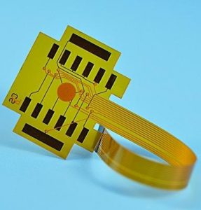
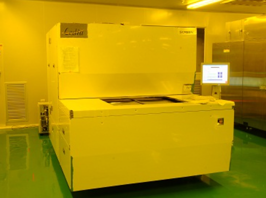
What is Laser Direct Imaging?
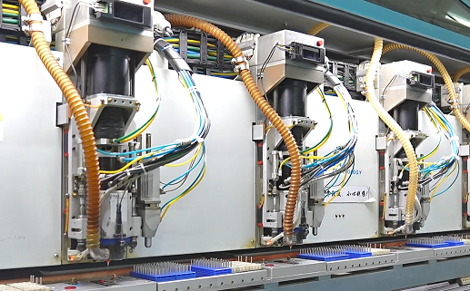
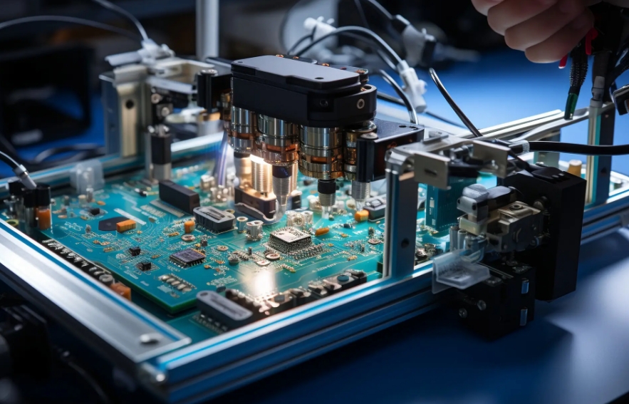
Laser Direct Imaging (LDI) is a technology that uses a laser beam emitted by an ultraviolet laser to image directly on a PCB (printed circuit board). Compared to traditional exposure techniques, LDI has higher image quality, precision traces and real-time adjustment.
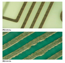
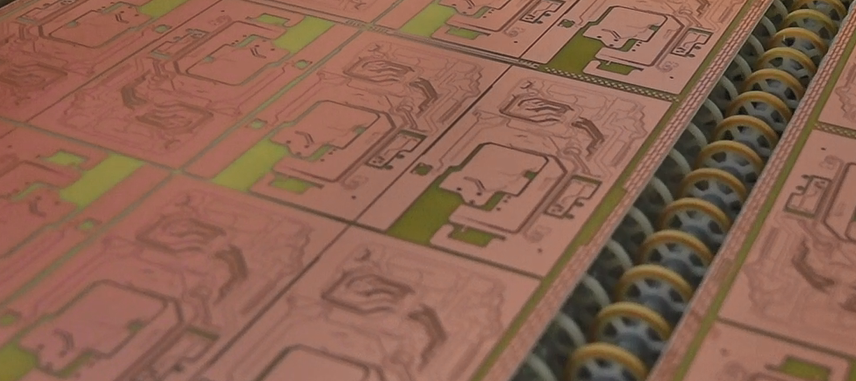
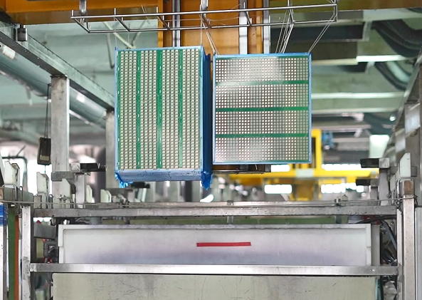
The LDI technology achieves pattern transfer by projecting the line image directly onto the PCB coated with photoresist through the laser beam emitted by the laser diode. This method eliminates the use of negatives in the traditional exposure process, reduces the time and cost of loading and unloading negatives, and avoids deviations caused by negative growing. The image resolution of LDI technology is high, and the fine wire can reach about 20um, which is suitable for the production of fine wire and improves the yield of PCB production.
Working Principle of LDI Technology
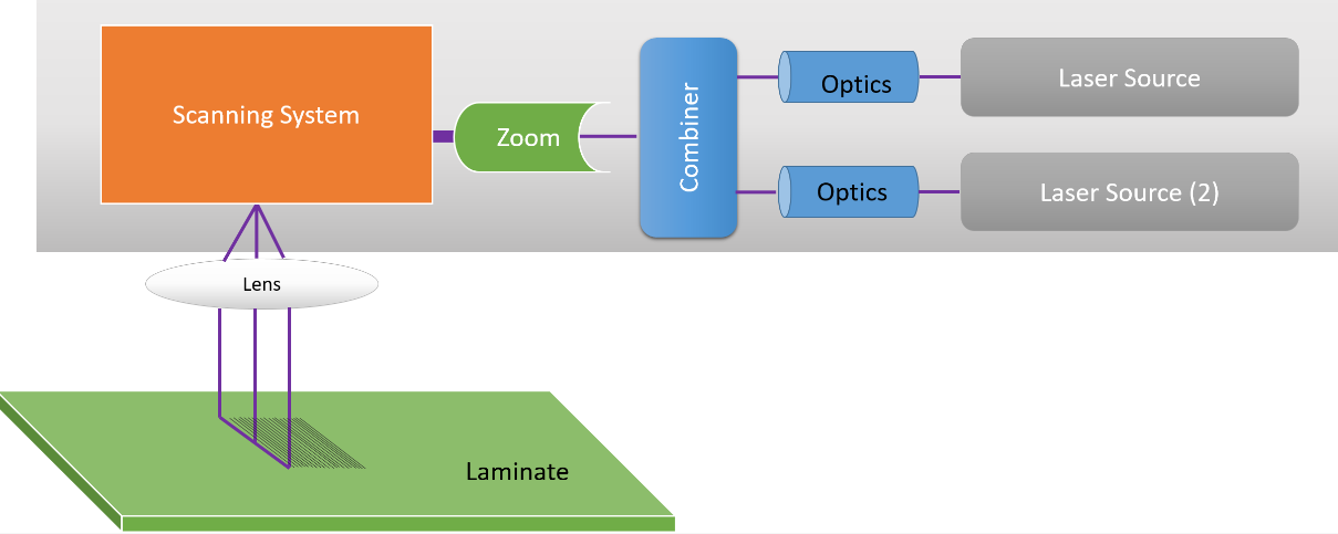
The principle of laser imaging is to acquire and present images based on the characteristics of laser beam. As we know, a laser is a highly focused, high-brightness, monochromatic beam that can therefore produce high-quality images. The laser imaging system mainly consists of laser, lens, scanning device and receiver. The laser is used to generate the laser beam, the lens is used to focus the beam, the scanning device is used to change the path of the beam on the object, and the receiver is used to receive the light signal and convert it into an image.
In the imaging process, the laser beam is focused from the laser through the lens, and then the path of the beam on the object is controlled by the scanning device. When the laser beam hits the surface of an object, it interacts with the surface. This interaction causes light to scatter and reflect, with scattered light diffusing in different directions and reflected light remaining in its original direction of propagation. The receiver receives the light scattered and reflected by the object and converts it into an electrical signal. The receiver converts the signal into a digital image signal, which is then processed and displayed on the screen to form an image. In the processing process, the received signal can be filtered, amplified and other operations to improve the quality and clarity of the image.
As PCB manufacturing processes continue to advance, LDI technology is also evolving. At present, the mainstream light source in the industry is the 405nm laser diode produced by Nichiya, Panasonic, and it is expected that the optical power requirements for exposure will be further improved in the future, and the optical power of a single device may develop to 100W. Nowadays, LDI technology is not only used in PCB manufacturing process, but also in high-end applications like medical imaging, industrial detection, remote sensing.
Advantages of Laser Direct Imaging Over Photo Exposure
The advantages of laser direct imaging (LDI) compared with traditional exposure machines mainly include the following aspects:
1. Eliminating the negative process in the exposure process
The LDI technology eliminates the step of making the negative in the traditional exposure process, thereby saving the time and cost of loading and unloading the negative, and reducing the deviation caused by the negative growth and contraction.
2. High resolution
The image resolution of LDI technology is very high, which is suitable for some very fine line production, especially for multi-layer PCB, which greatly improves the yield of PCB production.
3. High quality and precision
LDI is contactless operation, reducing the chance of miscontact, the closed operating environment reduces the influence of temperature and humidity, the image quality is high and fine, eliminating many defects in the traditional process.
4. Reduce errors and improve alignment
LDI technology improves alignment by eliminating alignment problems that often exist in photographic plates, especially the anisotropic movement of photographic plates caused by changes in temperature and humidity. High-precision alignment is achieved by using a charge-coupled device (CCD) camera system and a reference target to line up printed images and panels.
5. Shorten the production process and reduce costs
Because there is no need to have a negative production process, LDI technology shortens the production process, reduces the call of personnel, and reduces the production cost. In addition, the LDI system can lay more devices in the same environment, enabling two-way scanning and further savings.
6. Adapt to a variety of production needs
LDI technology has a flexible manufacturing route, which can meet various production needs without affecting the output. Once the data is delivered to the engineering department, production can begin, reducing product delivery time.
The image quality of LDI technology is clearer than that of traditional exposure technology, and it has obvious advantages in mid-to-high-end PCB manufacturing. With the transfer of global PCB production capacity to China and the high-end development of the electronics industry, the demand for LDI equipment continues to grow, and it is expected that the future will gradually replace traditional exposure equipment in the field of low-end PCB.
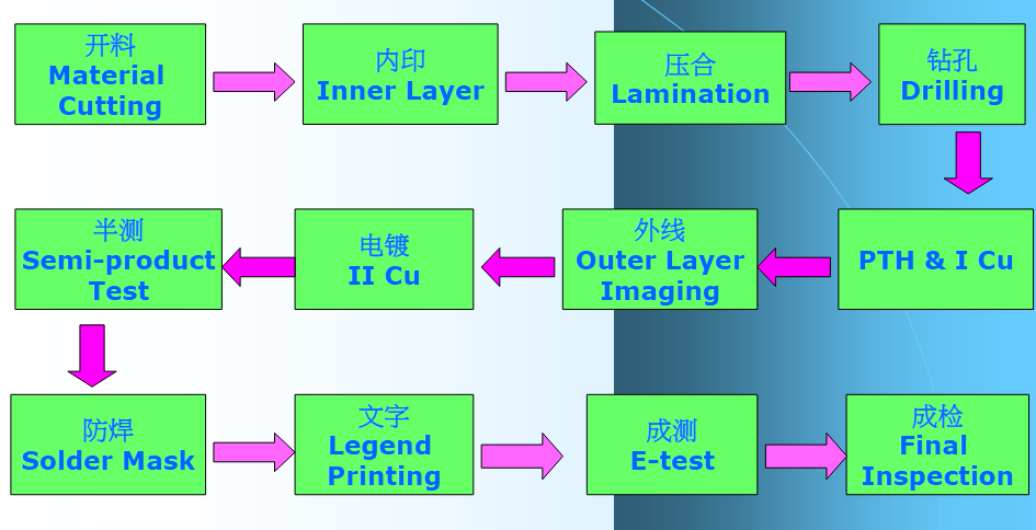
What is the Process of Direct Imaging?
Direct imaging with LDI involves several steps that ensure precise layer creation:
- Design Preparation: The digital circuit design is prepped for imaging, with adjustments made to accommodate laser processing specifics.
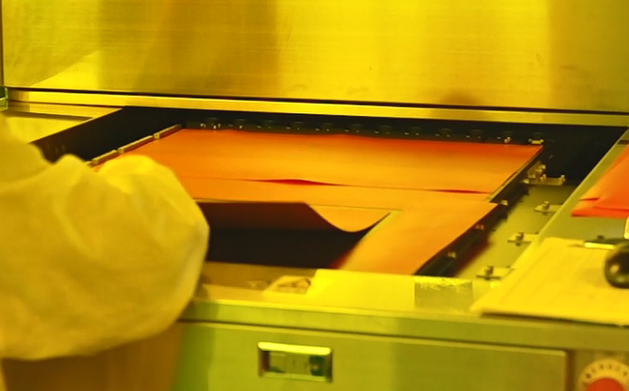
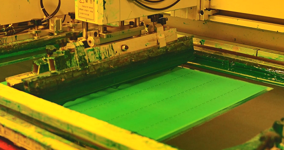
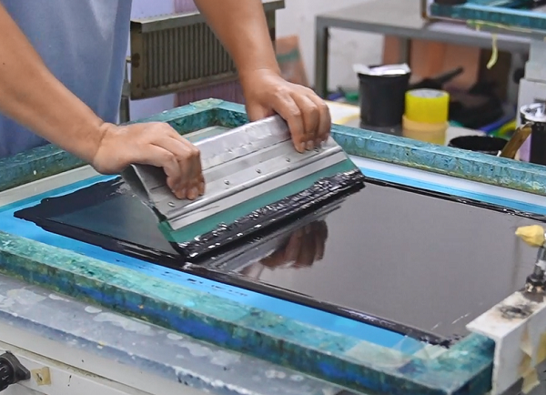
- Photoresist Coating: The PCB is coated with a light-sensitive photoresist material, which reacts chemically when exposed to the laser.
- Laser Imaging: The laser projects the circuit pattern directly onto the photoresist. Adjustments can be made mid-process, allowing for precise alignment.
- Developing: After exposure, the board is treated with a developer to reveal the circuit paths. Unexposed areas are removed, leaving only the intended design.
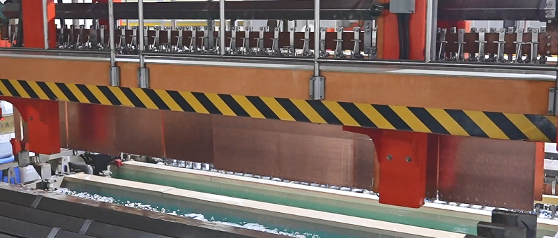
- Etching or Plating: Depending on the PCB type, the board undergoes etching or plating to define the copper traces, completing the imaging process.
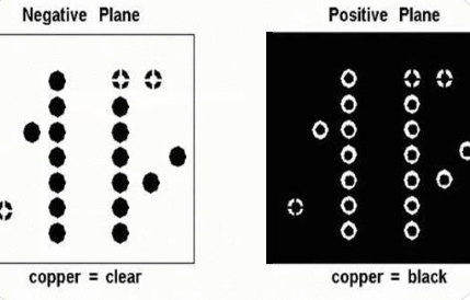
Difference Between Positive and Negative Images in PCB
In PCB photo exposure, the terms “positive” and “negative” refer to how the photoresist reacts to the laser exposure:
- Positive Image: Here, the laser exposes areas intended to be removed. During development, the exposed regions dissolve, leaving behind the unexposed areas as the design.
- Negative Image: In a negative image process, the laser exposes the regions meant to remain on the board. These exposed parts resist the developer, protecting the underlying material, while unexposed regions dissolve away.
The choice between positive and negative imaging depends on the photoresist type and the specific design requirements. Both methods offer high accuracy, but each has unique benefits based on the intended application.
Why LDI Process Less Cost-effective than Phototool?
While LDI offers many advantages, it often requires a higher initial investment than phototools:
1. Equipment Costs: LDI machines are sophisticated and costly, requiring a significant investment in laser technology and imaging systems.
2. Maintenance: High-precision lasers and optics demand regular maintenance and calibration to ensure consistent performance, which adds to operational costs.
3. Speed on Larger Runs: For high-volume production, phototools may still be more cost-effective. Phototools offer rapid replication without the need for repeated laser exposure, lowering costs for large-scale production.
These cost factors make LDI more suitable for specialized, lower-volume, or high-precision applications rather than large-batch productions.
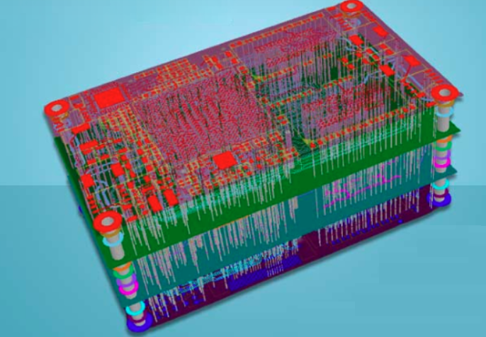
How is Layer Registration in LDI?
Layer registration is crucial in PCB manufacturing, especially for multilayer boards where each layer must align precisely. LDI excels in this aspect:
1. Automated Alignment: LDI systems come with advanced alignment software that adjusts each laser exposure to match the existing layer positions.
2. Reduced Human Error: Since the process is largely automated, human handling is minimal, reducing the risk of alignment issues.
3. Dynamic Adjustment: With real-time feedback systems, LDI machines adjust alignment during the process, maintaining tight registration tolerances.
If you’re seeking high-quality PCB manufacturing, consider choosing a provider skilled in LDI processes like Best Technology. Our company combines expertise with cutting-edge technology to ensure your boards are produced to exact specifications, delivering the durability and performance you need in today’s advanced electronics.