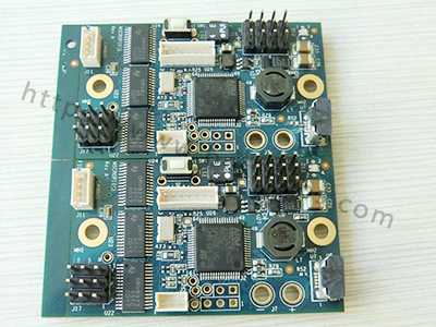
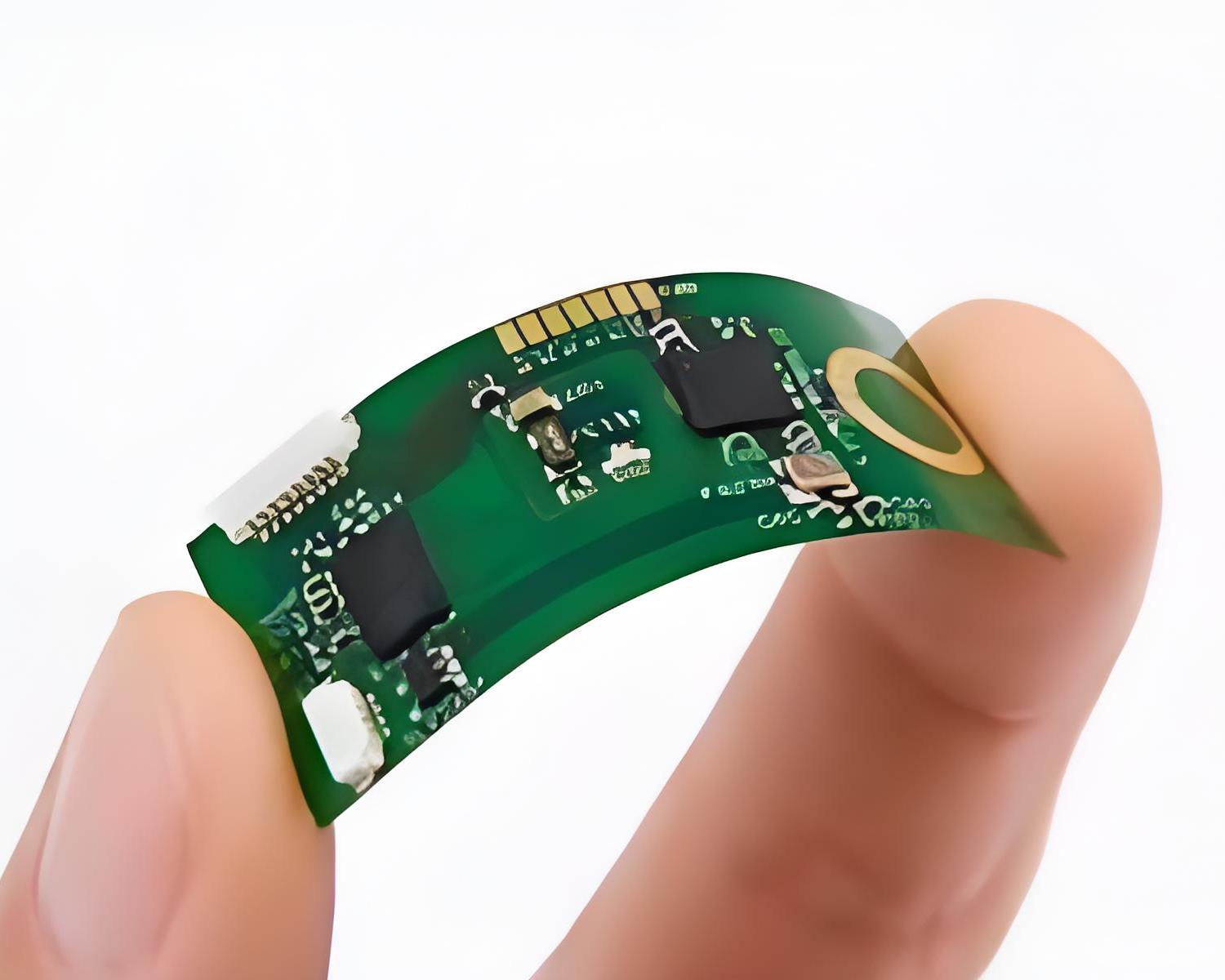
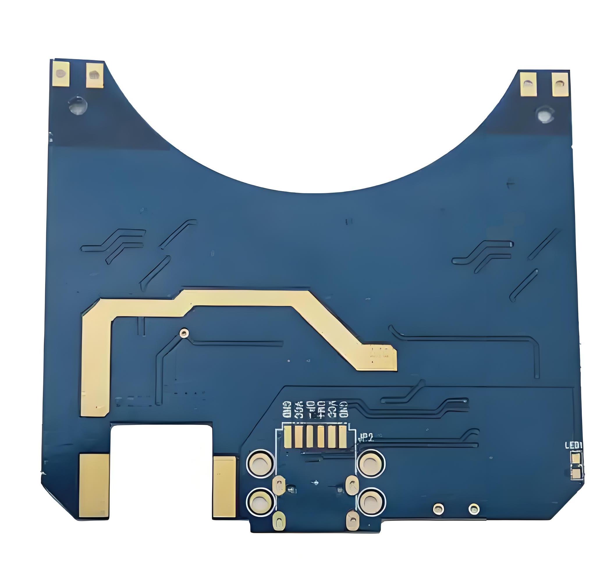
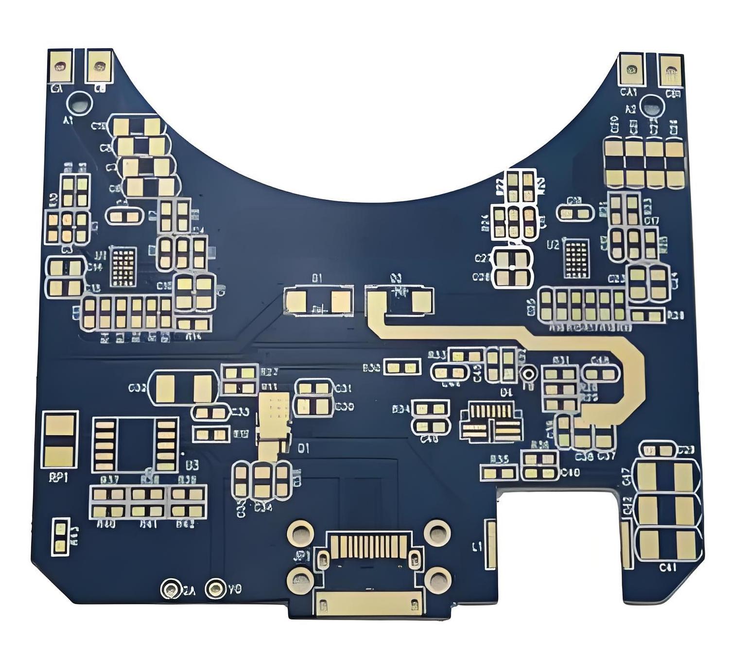
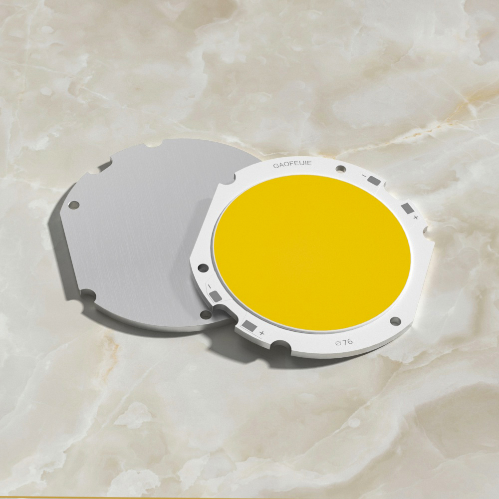
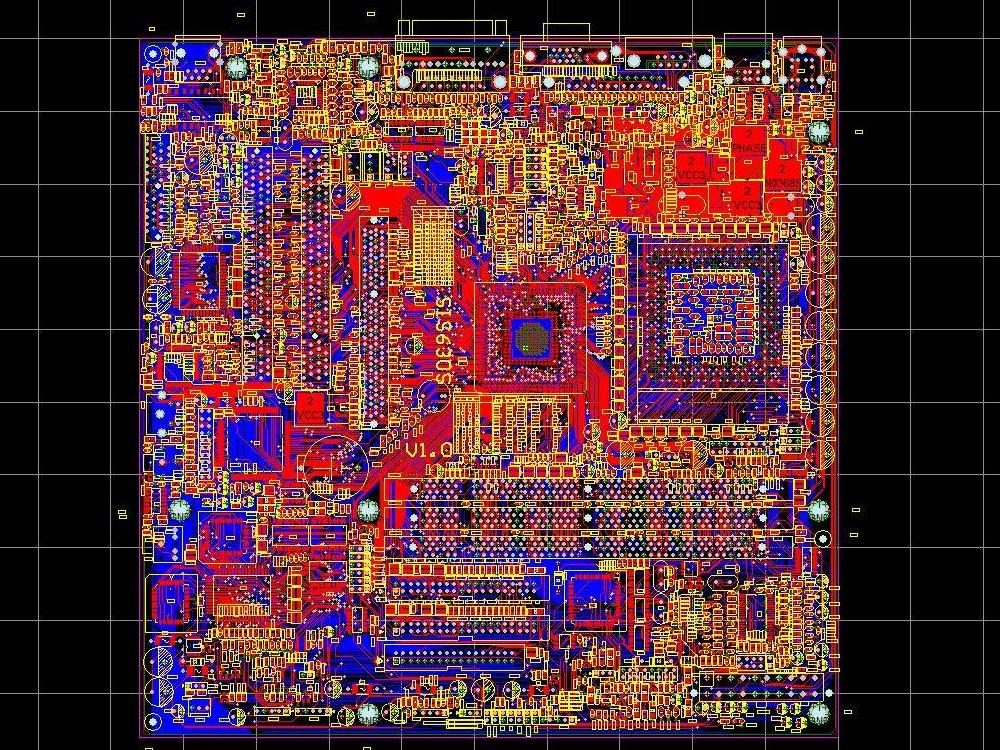
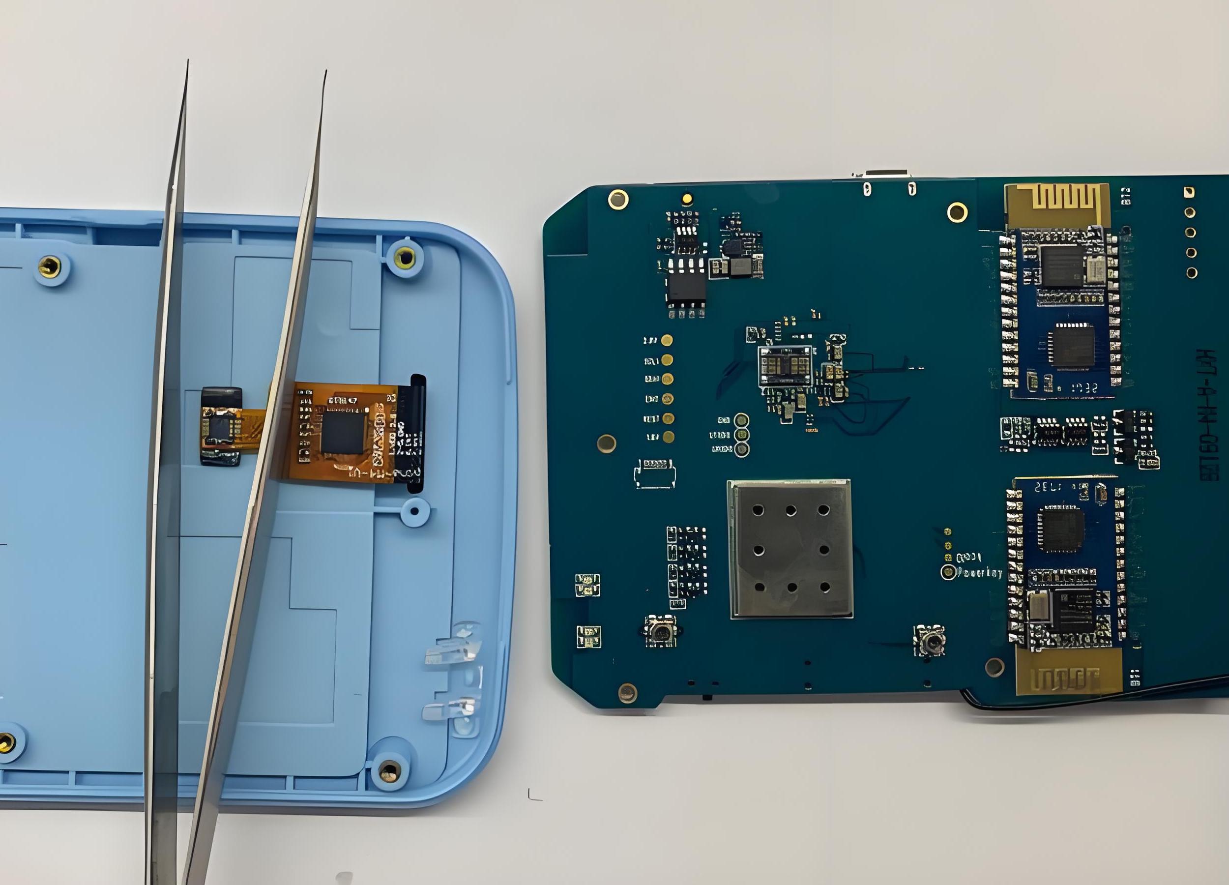
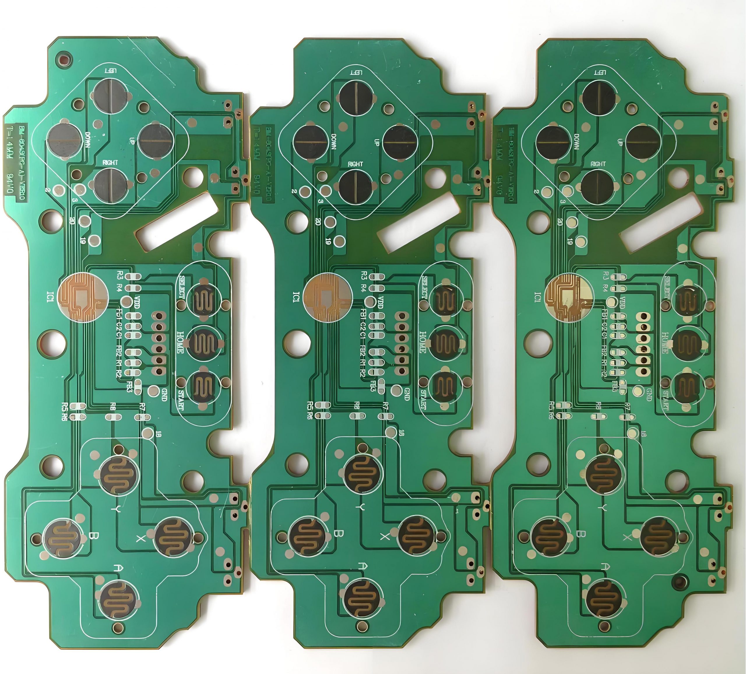
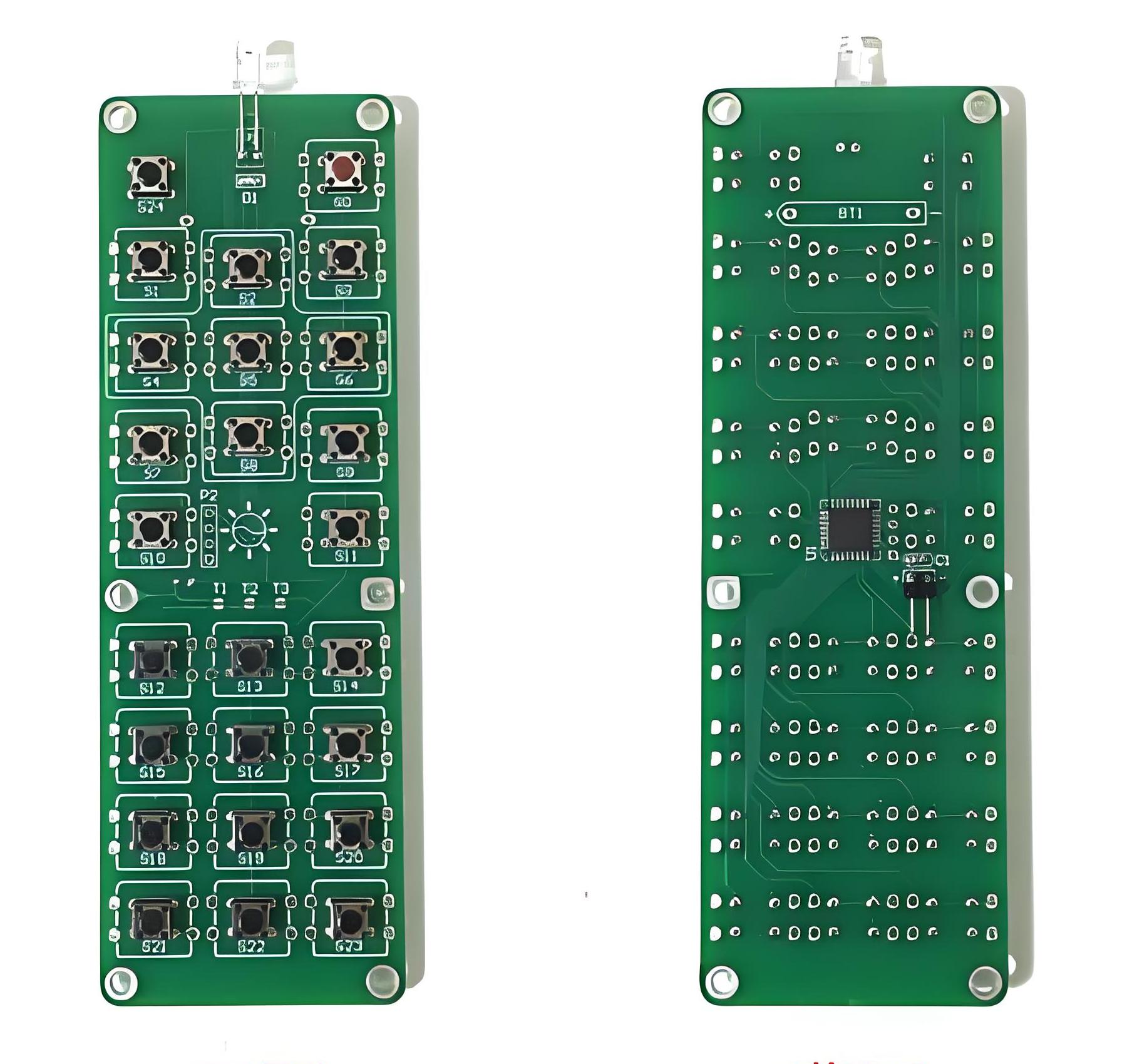
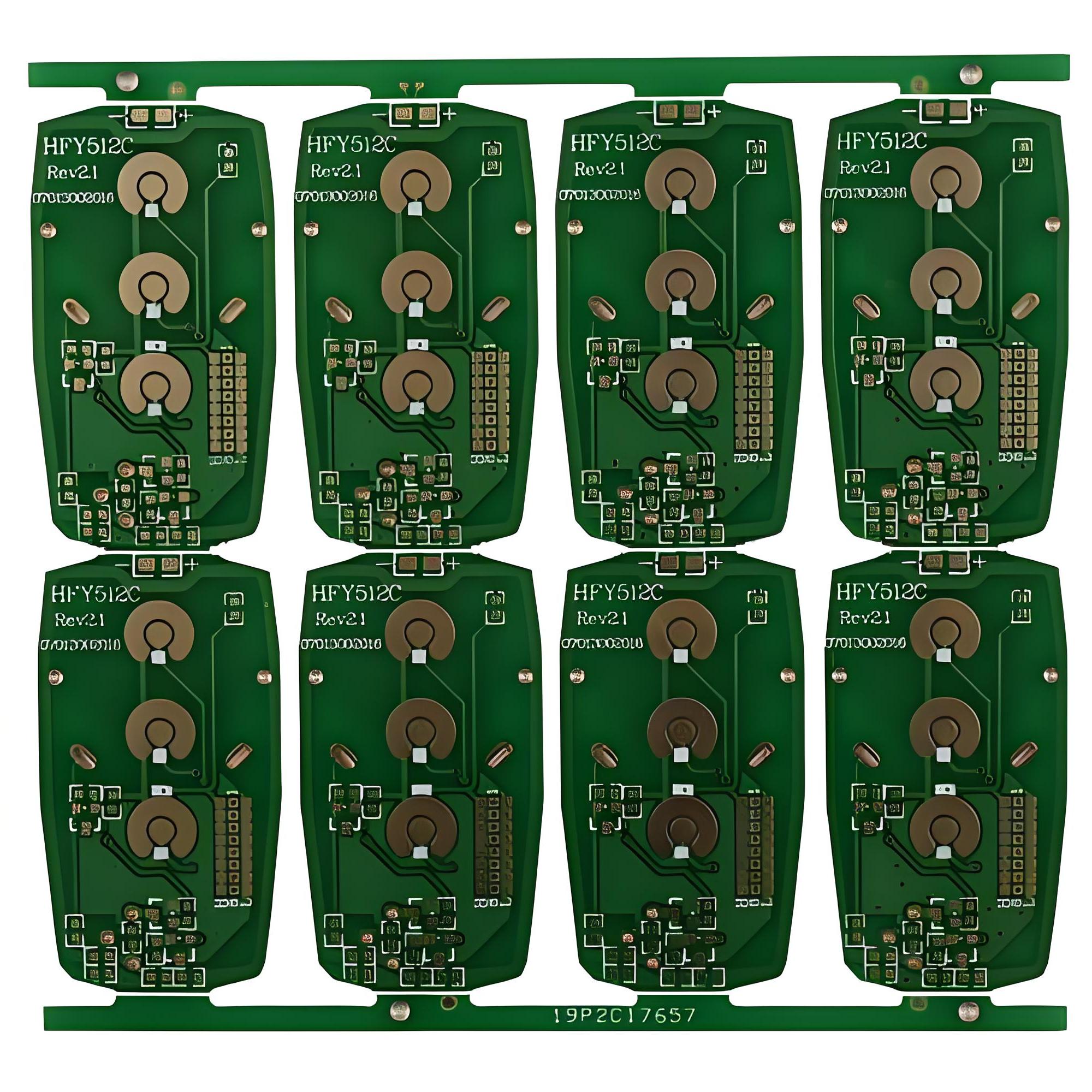
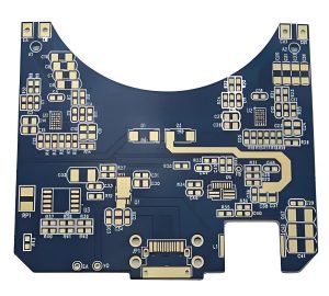
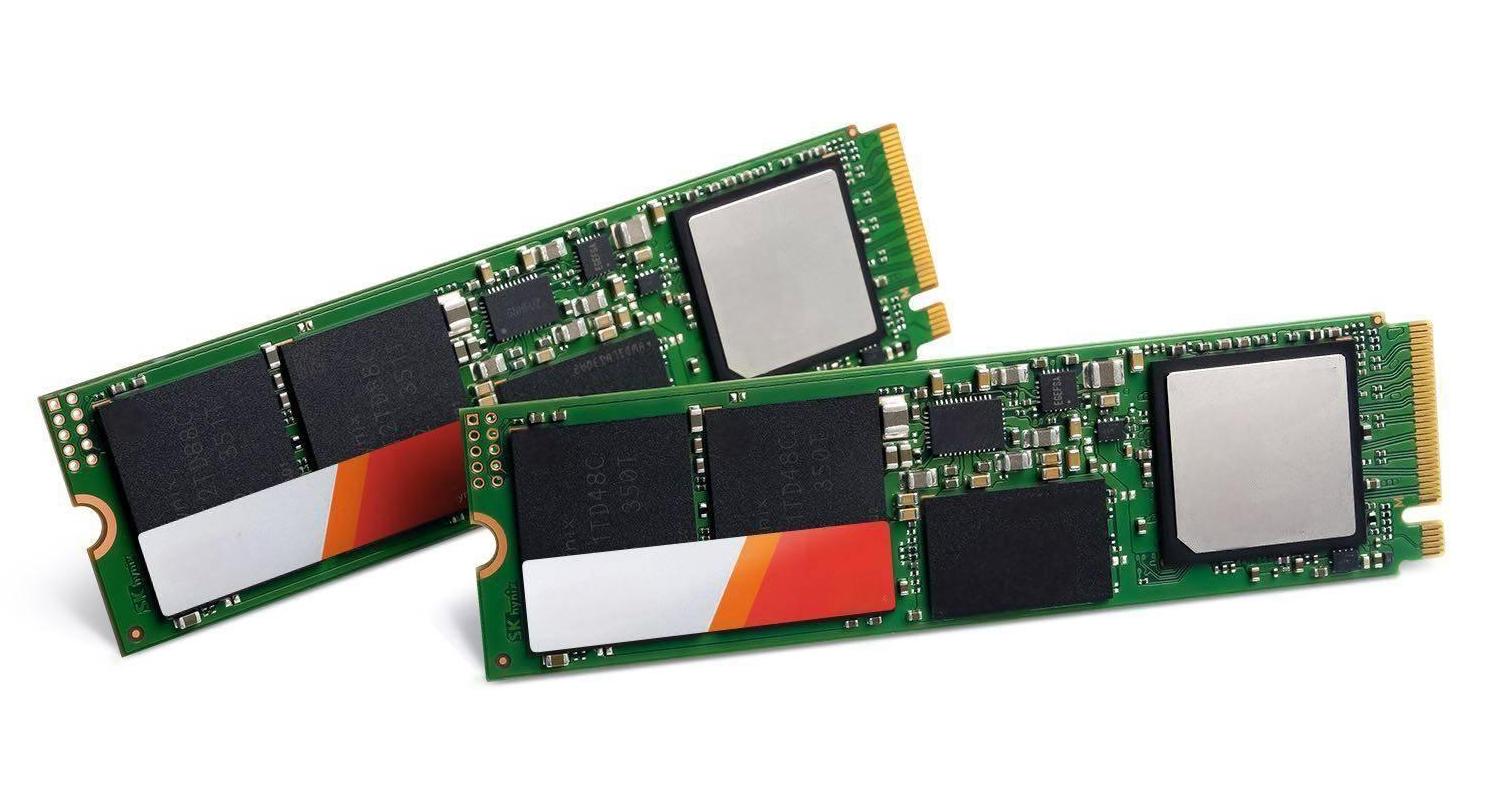
What is SSD PCB? SSD PCB is the core component of solid-state drives, used to connect and realize communication and data transmission between various components. It is usually composed of a multi-layer printed circuit board, integrating key components such as the main control chip, NAND flash chip, cache chip (some hard drives do not have DRAM), etc.
What is SSD PCB?
An SSD PCB is the printed circuit board that houses the essential components of a solid-state drive. It is designed to support NAND flash memory chips, a controller, and other electronic parts that allow the SSD to store and retrieve data efficiently.
The layout of the PCB directly impacts the drive’s performance, heat dissipation, and durability.
Modern SSD PCBs are engineered to handle high-speed data transfer and optimize energy efficiency. They are compact and lightweight, making them ideal for portable devices.
Additionally, advancements in PCB technology have enabled multi-layer designs, which improve performance and reliability.
What Does SSD Mean in Manufacturing?
In manufacturing, SSD stands for Solid-State Drive. It refers to a storage device that uses solid-state memory to store data, unlike traditional hard drives that rely on spinning disks.
SSD manufacturing involves assembling various components, including the PCB, memory chips, and controllers, into a compact and efficient storage solution.
The manufacturing process of SSDs requires precision and expertise. Each component must be carefully integrated to ensure optimal performance.
The PCB acts as the foundation, connecting all elements and ensuring seamless communication between them. Advanced techniques like surface-mount technology (SMT) are often used to create compact and reliable designs.
What is PCB in Hard Drive?
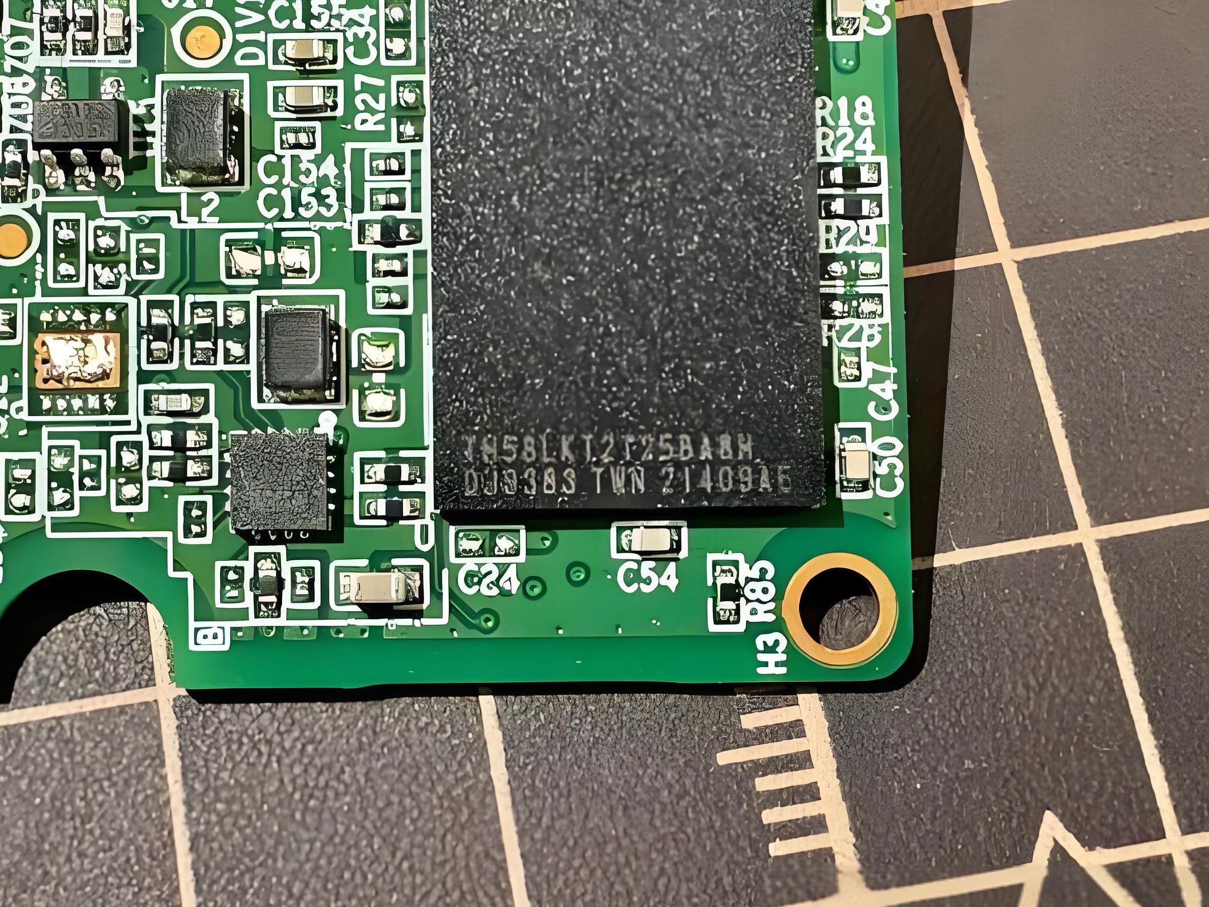
In both SSDs and traditional hard drives, the PCB serves as the foundational platform that connects all components. For SSDs, the PCB integrates NAND flash memory, a controller chip, and power management systems.
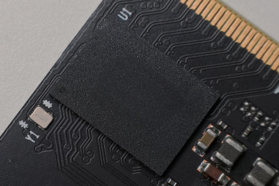
In hard disk drives (HDDs), the PCB also includes circuits that control the motor and read/write heads. SSD PCBs, however, are more advanced and compact due to their solid-state technology.
The role of the PCB in hard drives is crucial for data processing and management. In SSDs, the PCB’s design focuses on speed and energy efficiency, while in HDDs, it emphasizes mechanical control and data transfer. This distinction highlights the technological advancement of SSD PCBs over traditional HDD designs.
What Does SSD Stand For?
SSD stands for Solid-State Drive. The name highlights its design—no moving parts, unlike spinning disks in traditional HDDs. This architecture makes SSDs faster, more durable, and energy-efficient. They are widely used in laptops, desktops, and data centers due to their superior performance.
The term “solid-state” emphasizes the use of electronic circuits and memory chips instead of mechanical components. This innovation has revolutionized storage technology, making SSDs a preferred choice for modern applications.
How to Use an SSD in a PCB?
Using an SSD in a PCB involves designing a circuit board that accommodates NAND flash memory chips and a controller. Here are the key steps:
- Component Placement: Arrange NAND chips, a controller, and power management components on the PCB.
- Signal Integrity: Ensure proper signal routing to minimize interference and maximize performance.
- Thermal Management: Incorporate materials and designs to dissipate heat effectively.
- Power Management: Include circuits to regulate voltage and ensure stable operation.
- Testing: Validate the board’s functionality and reliability.
These steps require specialized tools and expertise to achieve optimal results. Advanced software tools are often used to simulate the PCB design and ensure it meets performance standards before production.
What are the Disadvantages of SSD?
While SSDs have numerous advantages, a few limitations exist:
- Higher Cost: SSDs are more expensive than HDDs per gigabyte.
- Finite Lifespan: NAND flash memory can only handle a limited number of write cycles.
- Capacity: Large-capacity SSDs are less common and pricier.
Despite these drawbacks, SSDs’ benefits far outweigh their disadvantages. The higher cost is offset by their speed, durability, and energy efficiency. Additionally, advancements in manufacturing have steadily reduced costs, making SSDs more accessible to consumers.
What is the Common Problem of SSD?
One common issue is data retention after prolonged use. Over time, SSDs may lose data due to wear on the NAND flash memory. This problem is minimized with advanced error correction codes (ECC) and wear-leveling technologies.
Another issue is sudden power loss, which can lead to data corruption. High-quality SSDs often include capacitors or other measures to mitigate this risk.
Manufacturers continuously innovate to address these challenges, ensuring modern SSDs are more reliable and durable than ever.
What is the Lifespan of an SSD?
Modern SSDs typically last 5 to 10 years, depending on usage and quality. Factors affecting lifespan include the number of write cycles and the type of NAND flash used. For instance, Single-Level Cell (SLC) SSDs last longer than Multi-Level Cell (MLC) or Triple-Level Cell (TLC) SSDs.
Regular backups and proper usage can extend an SSD’s life. Avoid excessive write operations and ensure the SSD’s firmware is updated regularly to maintain optimal performance. With proper care, SSDs can provide reliable storage for years.
Which Lasts Longer, SSD or HDD?
HDDs have mechanical parts prone to wear, while SSDs use solid-state memory, making them more durable under typical conditions.
However, HDDs may last longer in scenarios with infrequent data rewriting. SSDs’ durability, speed, and efficiency make them a better choice for most users.
The choice between SSD and HDD often depends on specific needs. For high-speed data access and portability, SSDs are superior. For long-term archival storage, HDDs might still be a viable option.
Why Choose Best Technology for SSD PCBs?
As a professional SSD PCB manufacturer, Best Technology brings unmatched expertise and experience to the table. With over 18 years in the PCB industry, we specialize in designing and fabricating high-performance SSD circuit boards. Our capabilities include:
- Advanced Materials: We use cutting-edge materials to ensure reliability and heat resistance.
- Precision Engineering: Our designs optimize performance and reduce signal interference.
- Global Facilities: With SMT factories in China and Vietnam, we provide cost-effective and scalable solutions.
- Customization: Tailored solutions to meet specific customer requirements.
- Quality Assurance: Rigorous testing to ensure every PCB meets industry standards.
Our commitment to quality ensures that your SSD PCBs meet the highest industry standards. Whether you need a prototype or large-scale production, we deliver exceptional results.
Conclusion:
SSD PCBs are the backbone of solid-state drives, enabling high-speed data storage and retrieval. Their design and manufacturing demand precision and expertise. Best Technology is a trusted partner for SSD PCB fabrication, offering advanced solutions tailored to your needs. For inquiries, reach out to sales@bestpcbs.com