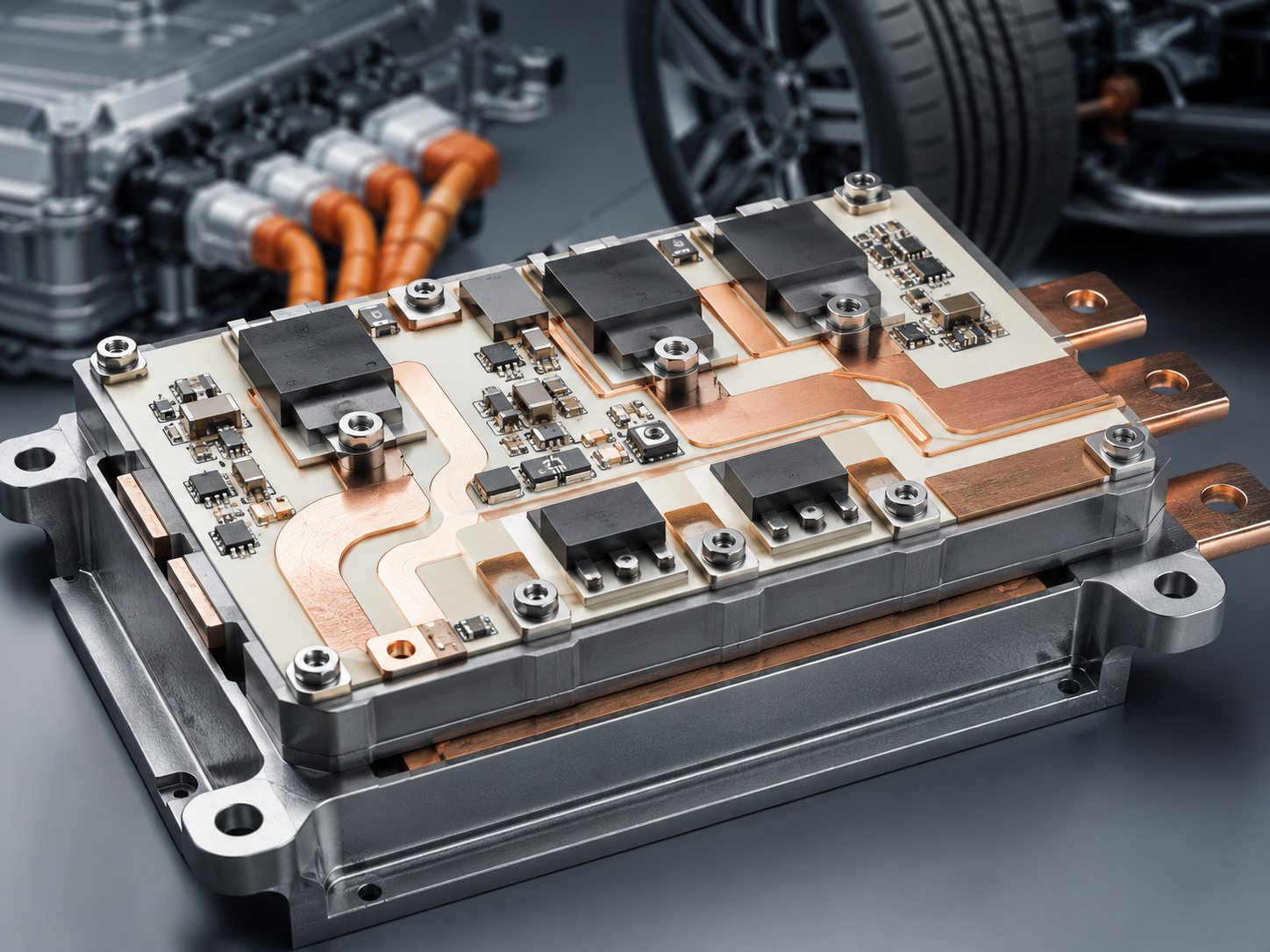
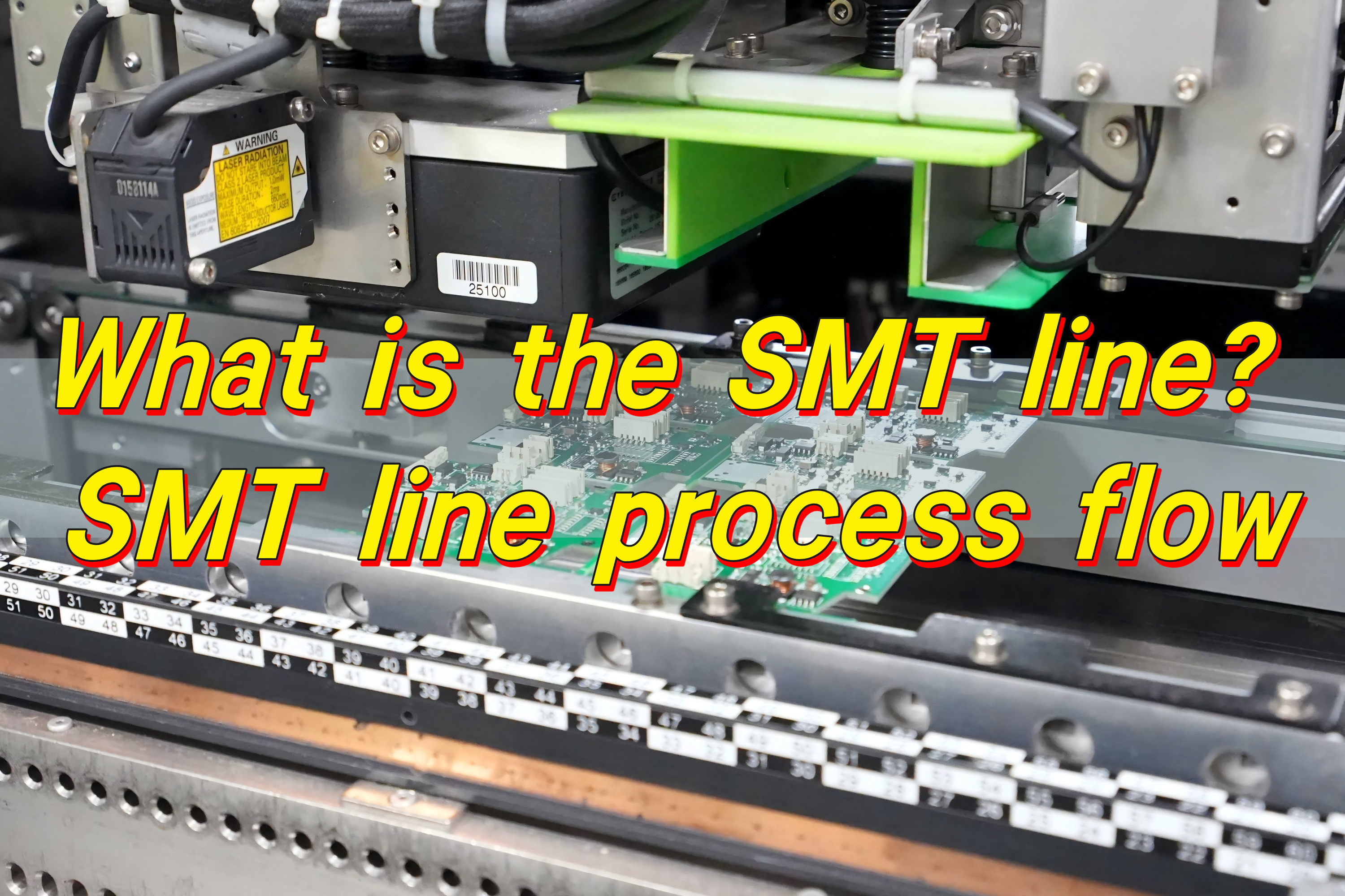
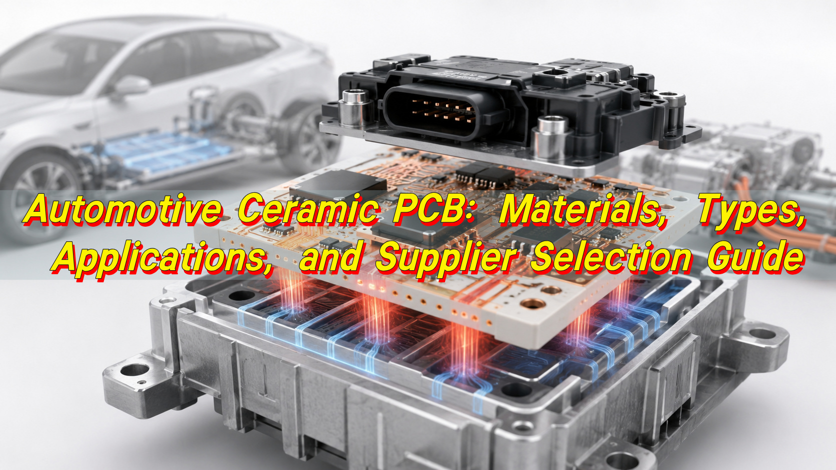
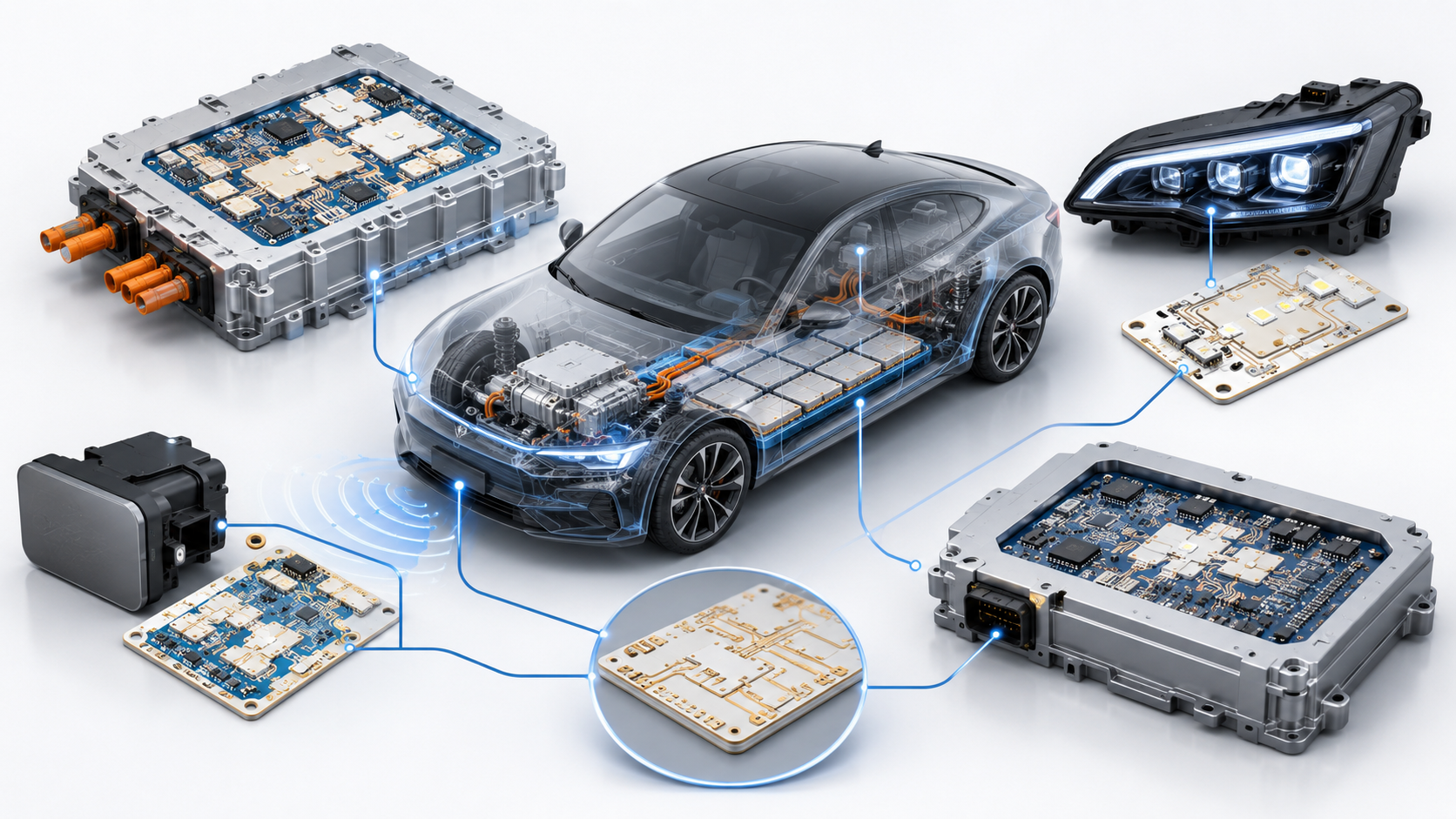
Automotive ceramic PCB technology is used when a vehicle electronic module needs stronger heat dissipation, better insulation, lower thermal expansion, and more stable performance than standard FR4 can provide. In electric vehicles, ADAS systems, LED headlights, battery control units, power modules, sensors, and high-current automotive PCB components, the circuit board is no longer just a connection carrier. It becomes part of the thermal path, electrical insulation system, and long-term reliability structure.
What Is an Automotive Ceramic PCB?
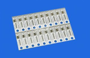
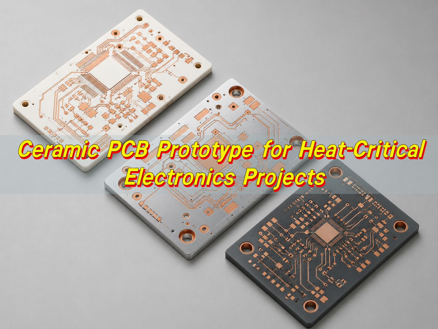
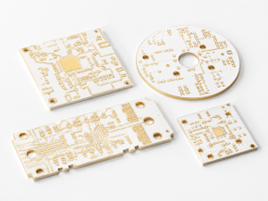
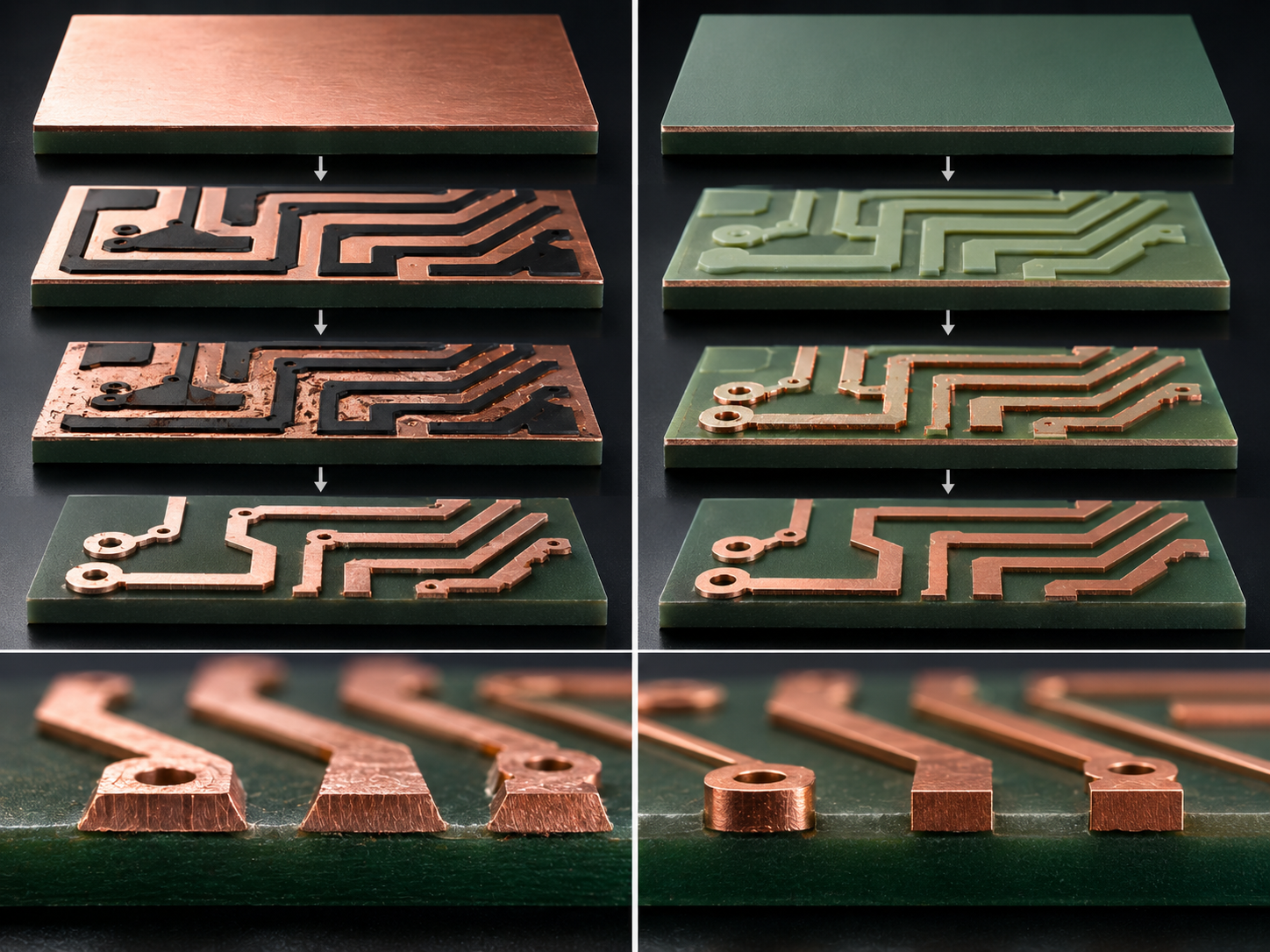
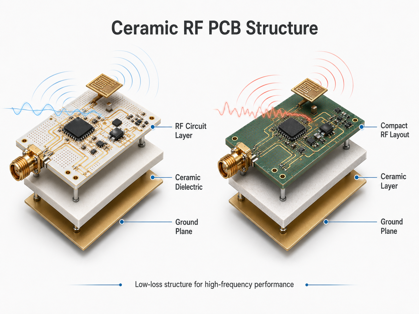
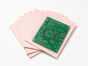
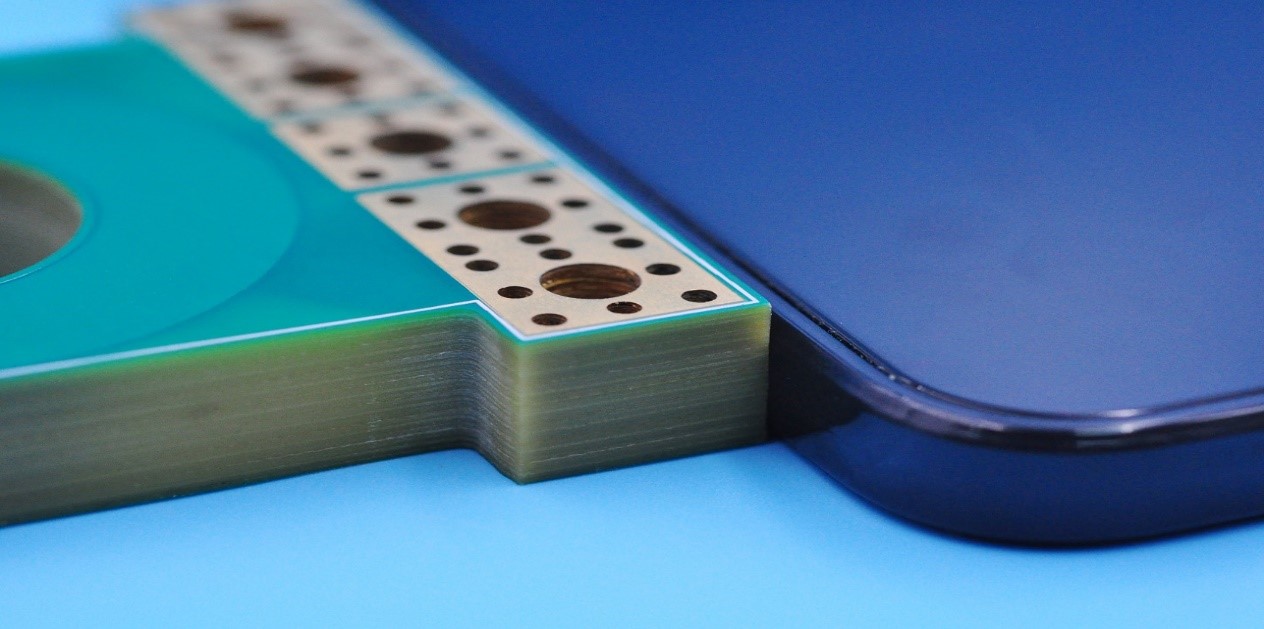
An automotive ceramic PCB is a printed circuit board that uses a ceramic substrate instead of conventional fiberglass-reinforced epoxy laminate. Common substrate materials include alumina, aluminum nitride, and silicon nitride. Copper circuitry is formed on the ceramic surface through processes such as DPC, DBC, AMB, thick film, or thin film manufacturing.
In automotive electronics, ceramic PCB is mainly used in modules exposed to heat, high power density, voltage stress, or repeated temperature changes. Typical examples include LED headlight boards, EV power conversion modules, battery-related control circuits, motor drive substrates, sensor modules, ignition-related electronics, and compact power control units.
Unlike FR4 PCB, ceramic PCB does not rely on organic resin as the main insulation base. This gives it better dimensional stability at high temperature, stronger thermal conductivity, and a coefficient of thermal expansion closer to many semiconductor materials. That is why many automotive PCB manufacturers use ceramic substrates for mission-critical thermal designs.
Why Are Ceramic PCBs Important in Automotive Electronics?
Modern vehicles contain more electronics than ever. EV platforms, hybrid systems, radar modules, high-brightness lighting, power converters, inverters, charging systems, and smart control units all create heat. At the same time, automotive modules must survive vibration, humidity, temperature cycling, current load, and long service life expectations.
Ceramic PCB helps solve several common automotive design problems:
- It moves heat away from power devices more efficiently.
- It provides stable electrical insulation under high voltage.
- It reduces thermal expansion mismatch between chips, copper, solder, and substrate.
- It supports compact layouts where heat sinks and thick FR4 structures are not enough.
- It improves reliability in modules that face repeated heating and cooling.
For buyers, this matters because thermal failure is often expensive. A board that works in a bench test may fail after months of real vehicle use if the substrate, copper thickness, solder joint, and thermal path were not designed together.
How Does an Automotive Ceramic PCB Work?
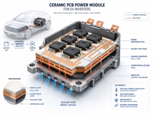
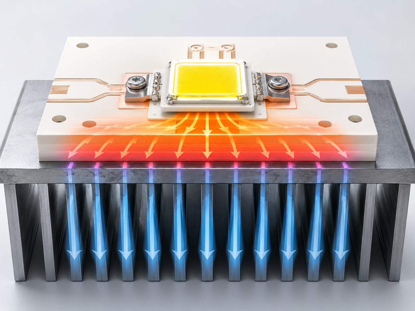
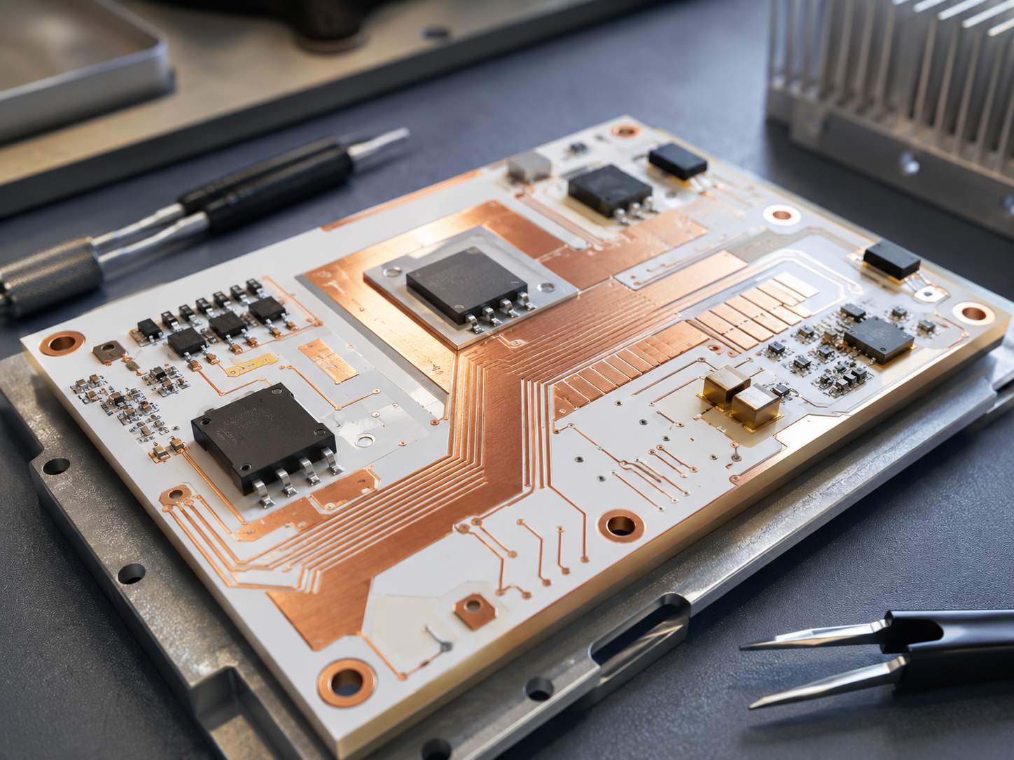
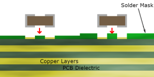
An automotive ceramic PCB works by combining electrical connection, insulation, and heat transfer in one structure. The ceramic substrate acts as an insulating but thermally conductive base. Copper traces or copper layers carry current and signals. Heat generated by power chips, LEDs, MOSFETs, IGBTs, resistors, or driver ICs is transferred through the copper and ceramic into the heat sink, housing, or cooling system.
The simplified thermal path is:
| Heat Source | Transfer Layer | Main Function |
|---|---|---|
| LED, MOSFET, IGBT, driver IC, resistor | Copper circuit layer | Current path and first heat-spreading layer |
| Ceramic substrate | Alumina, AlN, or Si3N4 | Electrical insulation and heat transfer |
| Interface material | Solder, sintered silver, thermal pad, or grease | Reduces thermal resistance |
| Heat sink or housing | Aluminum, copper, or module body | Final heat dissipation structure |
The performance depends on the whole stack, not only the ceramic material. A high-thermal-conductivity substrate cannot fully solve the problem if the copper is too thin, the solder layer has voids, the board is warped, or the heat sink contact is poor.
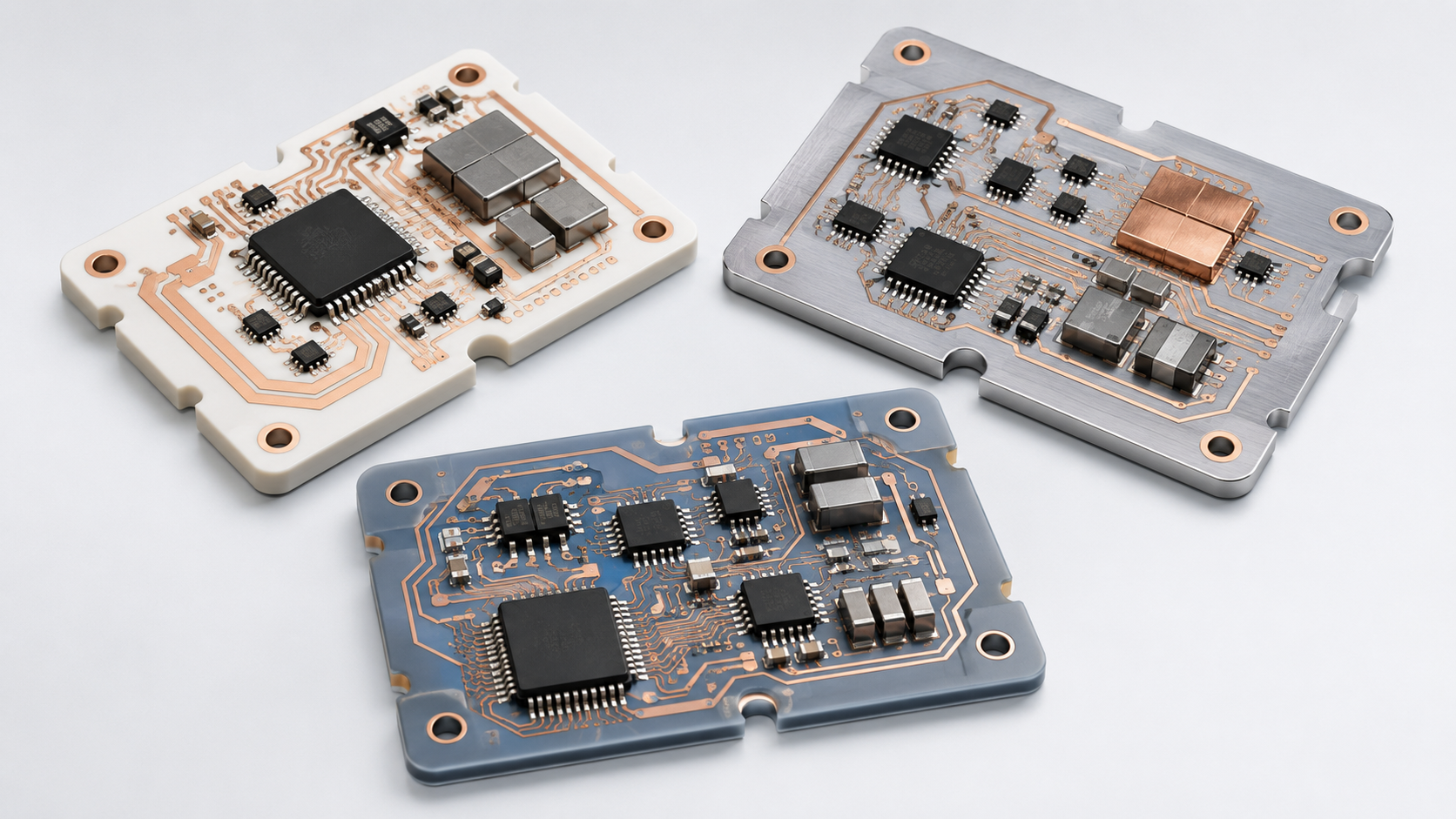
Main Automotive Ceramic PCB Types
Different automotive applications need different ceramic PCB structures. The most common options are DPC, DBC, AMB, thick film, thin film, HTCC, and LTCC.
| Type | Best Used For | Main Strength | Typical Limitation |
| DPC ceramic PCB | Fine circuits, sensors, LEDs, compact modules | Good circuit precision and plating control | Not ideal for very thick copper power modules |
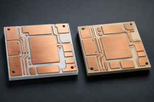
| DBC ceramic PCB | Power electronics, EV modules, high-current circuits | Strong copper thickness and thermal path | Less suitable for very fine traces |
| AMB ceramic PCB | EV power modules, Si3N4 substrates, high thermal cycling | Strong bonding and mechanical reliability | Higher cost and stricter process control |
| Thick film ceramic PCB | Resistor networks, sensors, hybrid circuits | Stable functional films and mature process | Limited fine-line capability |
| Thin film ceramic PCB | RF, precision sensors, high-frequency modules | Excellent precision and signal stability | Higher cost for mass production |
| HTCC | Harsh-temperature and sealed packages | Strong high-temperature structure | Process cycle is longer |
| LTCC | RF, antenna, sensor, multilayer ceramic modules | Good integration and miniaturization | Material and process matching are critical |
For automotive ceramic PCB selection, DBC and AMB are often considered for power modules, while DPC is more common for LED, sensor, and fine-circuit ceramic boards. Thick film and thin film ceramic PCB are chosen when functional resistive layers, precise metallization, or signal behavior matter.
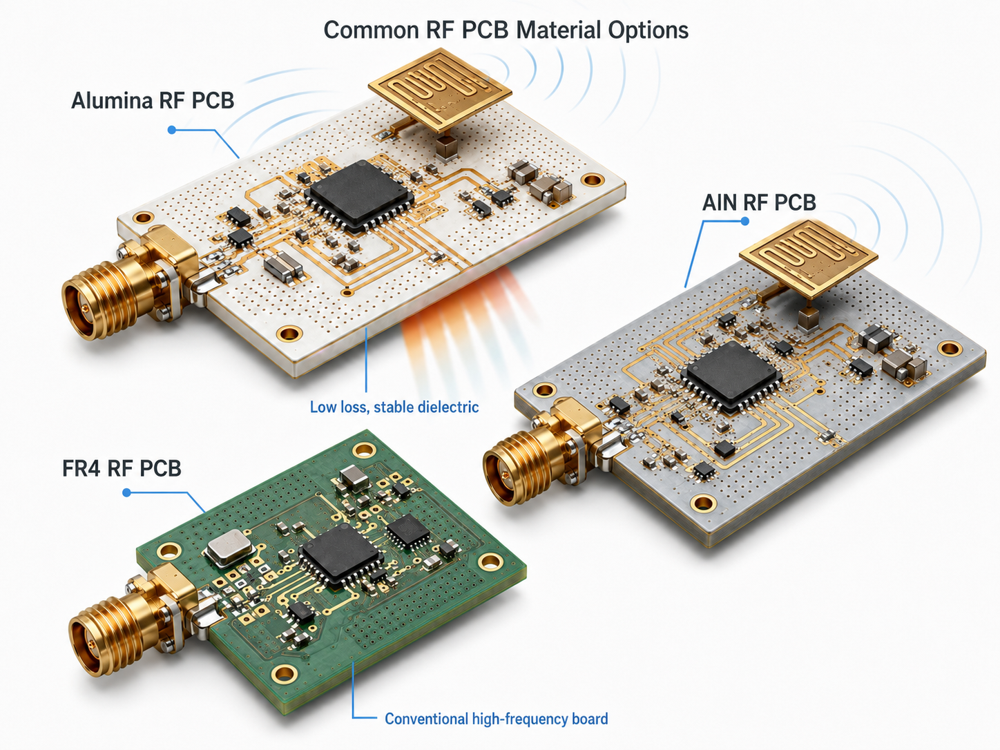
Ceramic PCB Materials Used in Automotive Applications
Material choice is one of the most important decisions in ceramic PCB design. The substrate affects heat transfer, mechanical strength, cost, thermal expansion, process compatibility, and long-term reliability.
| Material | Typical Thermal Conductivity | Typical Use in Automotive Electronics | Selection Note |
| Alumina ceramic | About 20–30 W/m·K | LED modules, sensors, moderate-power control boards | Cost-effective and widely used |
| Aluminum nitride | Often 170 W/m·K or higher | High-power LEDs, EV power modules, laser drivers, compact power boards | Strong thermal performance, higher material cost |
| Silicon nitride | Usually lower than AlN but mechanically strong | AMB power substrates, EV power cycling modules | Excellent strength and thermal shock resistance |
| Beryllium oxide | High thermal conductivity | Special high-performance uses | Limited by safety and processing concerns |
Alumina is often the practical starting point when cost control matters and the heat load is moderate. Aluminum nitride is preferred when thermal resistance must be reduced in a small space. Silicon nitride is valuable when mechanical robustness, thermal cycling, and copper bonding strength are more important than maximum thermal conductivity alone.
A good ceramic PCB manufacturer should not recommend the most expensive ceramic by default. The better approach is to match the substrate with junction temperature targets, voltage requirements, copper thickness, mounting method, and production volume.
Key Features and Benefits of Automotive Ceramic PCB
Automotive ceramic PCB offers several clear advantages when used in the right place.
| Benefit | Why It Matters in Vehicles |
| High thermal conductivity | Helps control LED brightness decay, MOSFET heating, and power module temperature |
| Electrical insulation | Supports compact high-voltage and high-current designs |
| Low thermal expansion | Reduces stress between chips, copper, solder, and substrate |
| High temperature resistance | Performs better than organic boards in hot zones |
| Good dimensional stability | Supports accurate assembly and stable module geometry |
| Strong corrosion resistance | Useful in sealed or harsh-environment electronics |
| Compact structure | Helps reduce module size in EV and smart vehicle systems |
The biggest benefit is not only heat dissipation. It is reliability under combined stress. Automotive modules rarely face just one stress factor. They often face heat, vibration, current load, humidity, and assembly pressure at the same time. Ceramic PCB can provide a stronger base for these demanding conditions.
Limitations and Risks You Should Know Before Selection
Ceramic PCB is powerful, but it is not suitable for every automotive board. FR4 is still the better option for many low-power control circuits, infotainment boards, general signal boards, and cost-sensitive modules.
Common limitations include:
- Higher material and manufacturing cost than FR4
- Brittleness during handling, routing, assembly, and module mounting
- Design restrictions for board size, panel utilization, and mechanical holes
- Longer production cycle for special materials or custom copper thickness
- Higher requirement for soldering profile, fixture design, and packaging protection
- Potential copper delamination if material, process, or thermal cycling is poorly controlled
The main mistake is using ceramic PCB as a direct FR4 replacement without redesigning the mechanical and thermal structure. Ceramic boards need careful attention to edge clearance, mounting pressure, copper balance, warpage, solder voids, and thermal interface contact.
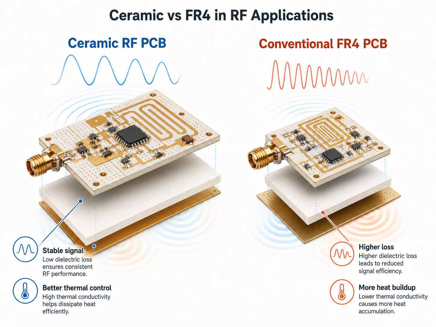
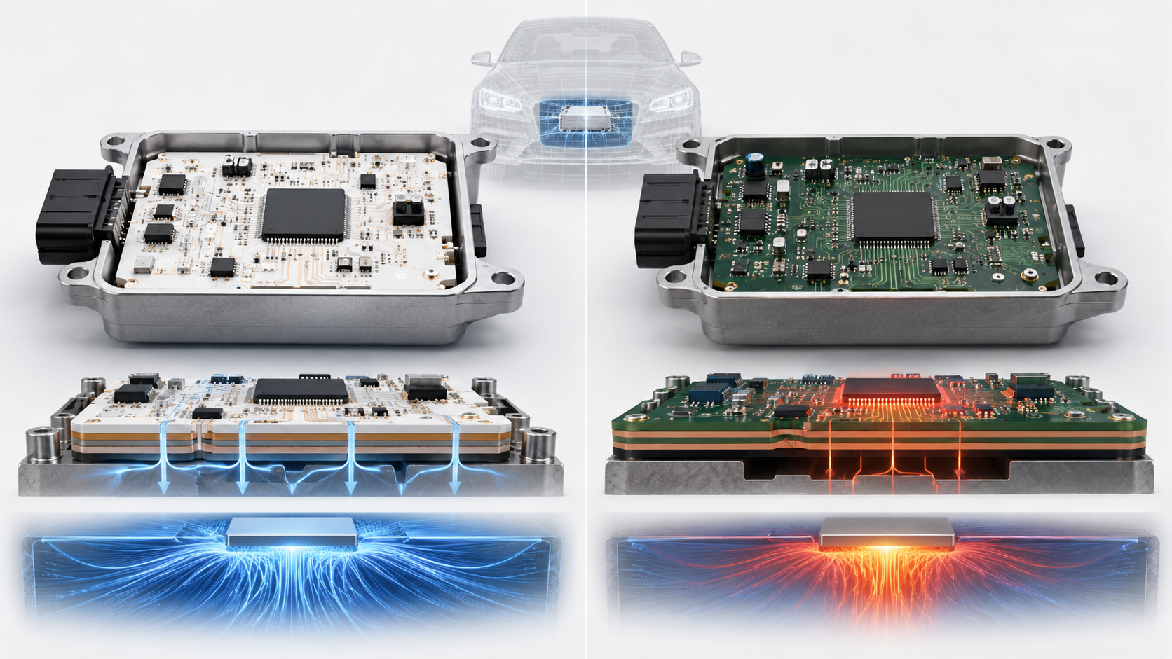
Ceramic PCB vs FR4 for Automotive Electronics
Ceramic PCB vs FR4 is one of the most common comparison topics for automotive engineers and buyers. The correct answer depends on the heat load, voltage level, reliability target, cost range, and application zone.
| Item | Ceramic PCB | FR4 PCB |
| Base material | Alumina, AlN, Si3N4, or other ceramic | Fiberglass-reinforced epoxy laminate |
| Thermal performance | Much higher | Limited |
| Electrical insulation | Strong | Good for standard applications |
| High-temperature stability | Strong | Depends on Tg and resin system |
| Mechanical toughness | Brittle, needs careful handling | Better flexibility and toughness |
| Fine multilayer routing | Possible but costlier | Mature and cost-effective |
| Cost | Higher | Lower |
| Best fit | Power, LED, EV, sensor, high-heat modules | General control, communication, logic, low-power boards |
Use ceramic PCB when heat, insulation, or thermal cycling is the core reliability issue. Use FR4 when the board mainly handles low-power signals, standard control logic, or cost-sensitive assembly. In many automotive products, both materials can appear in the same system. A power section may use ceramic PCB, while the control section remains FR4.
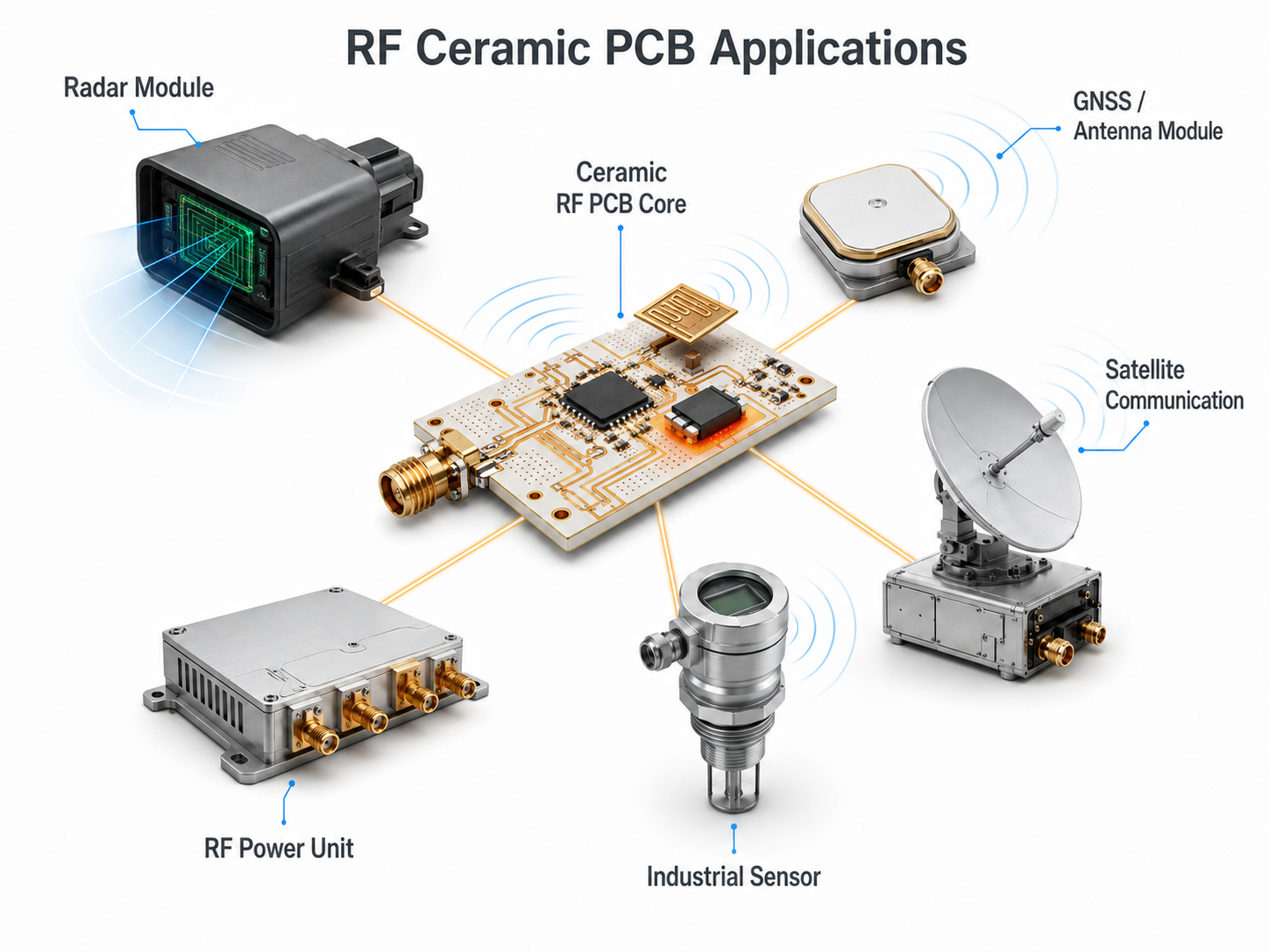
Where Are Automotive Ceramic PCBs Used?
Automotive ceramic PCB is used across several high-value vehicle electronics areas.
EV power electronics
Ceramic substrates are used in inverters, DC-DC converters, onboard chargers, power modules, and current control circuits. These applications need strong insulation and heat transfer.
LED headlights and lighting modules
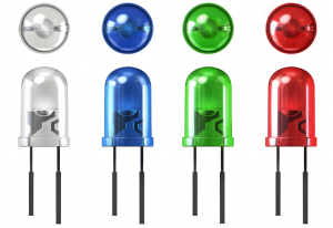
High-power LED headlights generate concentrated heat. Ceramic PCB helps keep LED junction temperature under control and supports long-term brightness stability.
Battery management and high-voltage control
Some battery-related circuits need insulation stability, heat resistance, and reliable current handling. Ceramic boards can support compact layouts near high-power zones.
ADAS sensors and radar-related modules
Sensor modules may require stable dimensions, low signal loss, and thermal stability. Thin film or LTCC ceramic solutions may be considered in selected high-frequency or sensor packaging designs.
Engine and transmission control environments
Near-engine electronics face heat and vibration. Ceramic PCB can be used where standard boards may struggle with temperature cycling.
Automotive power resistors and hybrid circuits
Thick film ceramic PCB is useful for resistor networks, hybrid circuits, and compact modules requiring printed resistive elements.
Practical Automotive Case Examples
A useful way to understand ceramic PCB is to look at realistic engineering scenarios.
| Case | Original Problem | Ceramic PCB Solution | Result |
| LED headlight module | FR4 board caused high LED temperature and faster lumen decay | Alumina or AlN ceramic PCB with optimized copper area | Better heat spreading and more stable lighting performance |
| EV power module | High current created hot spots and solder fatigue risk | DBC or AMB ceramic substrate with thick copper | Lower thermal resistance and stronger power cycling reliability |
| Sensor module | Signal drift appeared after repeated temperature exposure | Thin film or precision ceramic substrate | Improved dimensional and electrical stability |
| Compact DC-DC board | Limited space made metal heat sink design difficult | AlN ceramic PCB integrated into heat path | Higher power density in a smaller module |
| High-temperature hybrid circuit | Organic substrate could not support operating zone | Thick film ceramic circuit | More stable long-term operation |
These cases show one important point: ceramic PCB is selected to solve a specific bottleneck. It should be introduced when the thermal path, insulation demand, or environmental stress makes standard PCB materials less suitable.
Design Guidelines for Automotive Ceramic PCB
A strong automotive ceramic PCB starts with design decisions made before manufacturing. Engineers should not treat ceramic as only a material upgrade. The layout, copper geometry, substrate thickness, component placement, and mechanical mounting all affect reliability.
Key design points include:
- Place high-heat components close to the main thermal path.
- Avoid sharp copper corners where stress can concentrate.
- Keep copper distribution balanced to reduce warpage.
- Reserve safe edge clearance because ceramic edges are more fragile than FR4.
- Control hole placement and avoid unnecessary mechanical stress points.
- Match copper thickness with current load and heat-spreading needs.
- Review solder pad size carefully to control voiding and wetting.
- Define voltage clearance based on working voltage and pollution environment.
- Confirm mounting torque, screw position, and support structure early.
- Use DFM review before prototype production.
For automotive projects, the drawing should clearly specify substrate material, copper thickness, board thickness, surface finish, tolerance, flatness, test requirements, and packaging method. Missing details can create serious problems when the project moves from sample development to batch production.
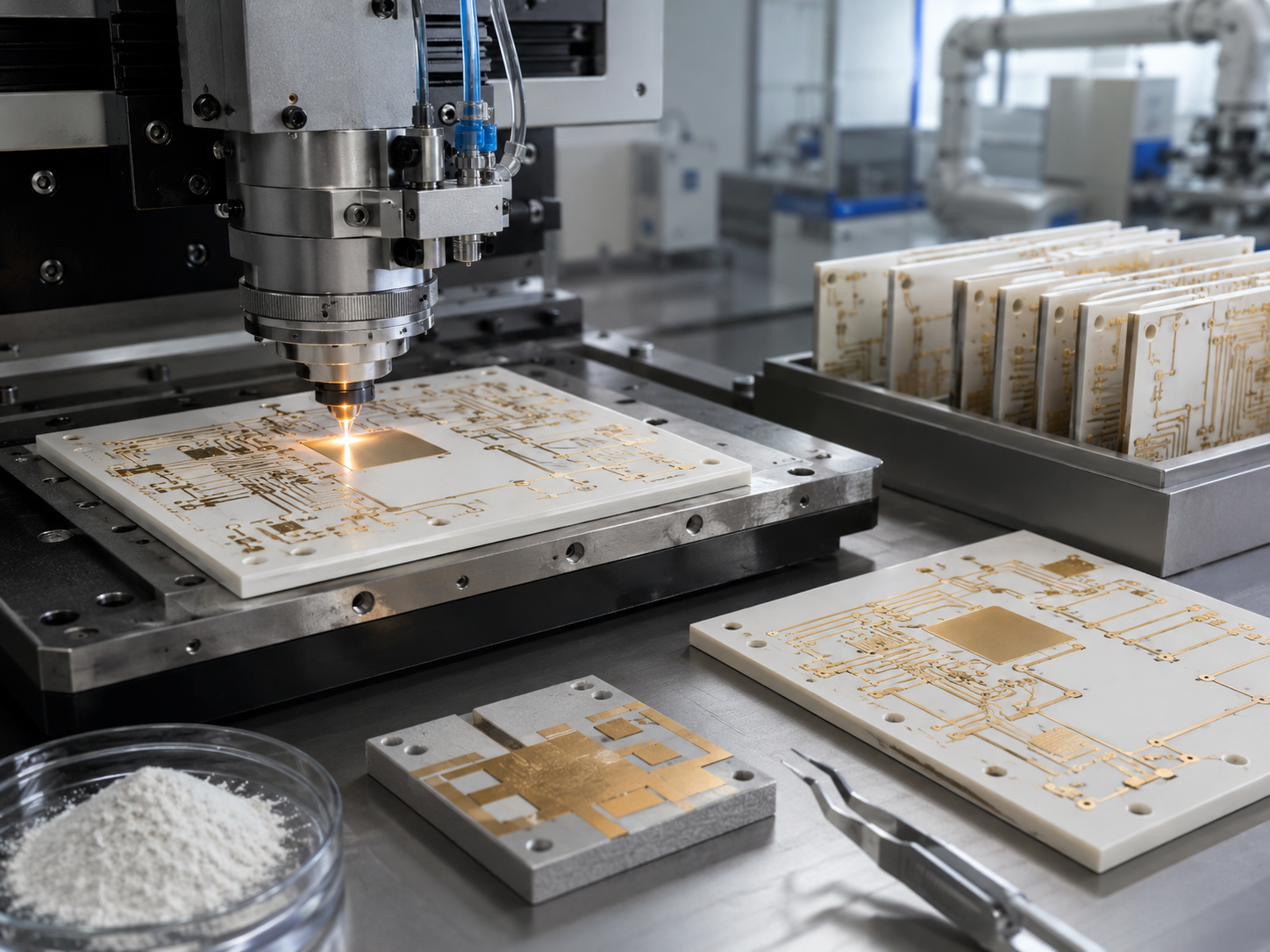
Manufacturing Process Considerations
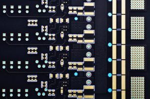
Automotive ceramic PCB manufacturing requires tighter process control than standard FR4 PCB. The right process depends on the required copper thickness, line width, substrate type, and reliability target.
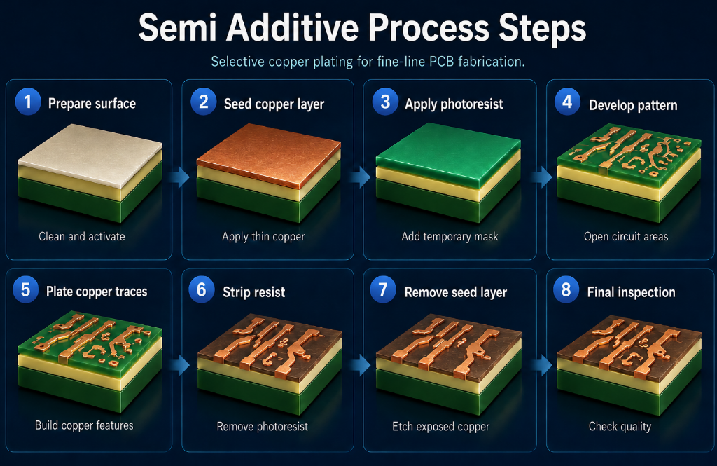
DPC process usually involves ceramic cleaning, seed layer deposition, imaging, copper plating, etching, solder mask or protective layer, surface finish, profiling, and final testing. It is suitable for fine circuits and medium copper thickness.
DBC process bonds copper directly to ceramic under high temperature. It is often used for power substrates with thicker copper and strong thermal transfer.
AMB process uses active brazing material to bond copper and ceramic, especially for silicon nitride substrates. It is suitable for high-reliability power modules and harsh thermal cycling conditions.
Thick film process prints conductive, resistive, or dielectric paste on ceramic and fires it at high temperature. It is useful for hybrid circuits and functional layers.
Thin film process uses vacuum deposition and photolithography for very precise circuits. It is common in high-frequency, sensor, and precision electronic modules.

Manufacturing quality depends on ceramic surface preparation, copper adhesion, plating uniformity, sintering or bonding control, etching accuracy, flatness, edge quality, and final cleaning. For automotive applications, process stability is often more important than a single impressive parameter.
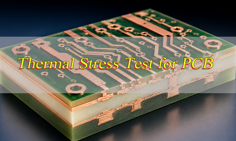
Testing Methods and Quality Control
Automotive ceramic PCB quality control should cover electrical, thermal, mechanical, and visual reliability. A simple open-short test is not enough for critical vehicle modules.
Common testing and inspection items include:
| Test or Inspection | Purpose |
| Electrical open-short test | Confirms basic circuit continuity and isolation |
| Hi-pot test | Checks insulation under high voltage |
| AOI | Detects line defects, scratches, contamination, and pattern issues |
| X-ray inspection | Reviews voids, bonding, or internal defects in selected assemblies |
| Thermal cycling test | Evaluates stress under repeated temperature changes |
| Copper adhesion test | Checks bonding strength between copper and ceramic |
| Warpage and flatness measurement | Supports stable assembly and heat sink contact |
| Microsection analysis | Reviews copper thickness, plating quality, and interface structure |
| Ionic contamination test | Helps reduce corrosion and leakage risk |
| Final visual inspection | Checks edge cracks, chipping, stains, and surface defects |
For automotive PCB suppliers, quality control should also include lot traceability, material certificates, process records, inspection reports, and controlled packaging. This is especially important for OEM, ODM, and batch production projects where repeatability matters more than one successful prototype.
Common Failure Modes and Factory-Level Prevention
Automotive ceramic PCB failures usually come from the interaction of material, design, assembly, and operating stress.
| Failure Mode | Common Cause | Prevention Method |
| Ceramic cracking | Excess mounting force, poor fixture support, edge impact | Control torque, improve panel handling, add support structure |
| Copper delamination | Weak bonding, thermal shock, poor material match | Select proper DBC/AMB/DPC process and verify adhesion |
| Solder joint fatigue | CTE mismatch and repeated thermal cycling | Optimize pad design, solder profile, and component placement |
| Hot spots | Poor thermal path or insufficient copper area | Improve copper spreading, substrate selection, and heat sink contact |
| Insulation breakdown | Contamination, insufficient clearance, high voltage stress | Improve cleaning, spacing, coating, and hi-pot testing |
| Warpage | Unbalanced copper, process stress, thin substrate | Balance copper and control firing/bonding process |
| Surface contamination | Poor cleaning or packaging | Add cleanliness inspection and vacuum or dry packaging |
A strong ceramic PCB manufacturer should be able to discuss these failure modes before production, not only after defects appear. For automotive projects, prevention is always cheaper than field failure analysis.
Cost Factors in Automotive Ceramic PCB
Automotive ceramic PCB cost is affected by material, board size, copper thickness, process type, tolerance, surface finish, test requirements, and order volume.
Main cost drivers include:
- Ceramic material: AlN and Si3N4 usually cost more than alumina.
- Process type: AMB and thin film are generally more expensive than basic alumina DPC.
- Copper thickness: thicker copper increases material and processing difficulty.
- Circuit precision: fine lines and tight spacing require stricter control.
- Board size: larger ceramic panels are harder to process and protect.
- Surface finish: ENIG, ENEPIG, silver, and other finishes affect cost.
- Testing level: thermal cycling, hi-pot, cross-section, and reliability tests add cost.
- Yield risk: complex structures and tight tolerances may reduce production yield.
- Packaging: automotive ceramic boards need stronger protection during shipping.
The best cost strategy is not to choose the cheapest substrate. It is to define the real working conditions and avoid over-specification. For example, alumina may be enough for a moderate-power LED board, while AlN may be necessary for a compact high-power module. Using AlN where alumina is sufficient increases cost without adding meaningful value.
How to Choose a Ceramic PCB Manufacturer for Automotive Projects?
Choosing a ceramic PCB manufacturer is not only about unit price. Automotive projects need engineering support, process stability, documentation, and repeatable quality.
A qualified supplier should be able to support:
- Alumina, aluminum nitride, and selected silicon nitride ceramic substrates
- DPC, DBC, AMB, thick film, or other suitable manufacturing processes
- Prototype development and batch production transfer
- Material traceability and incoming inspection
- Copper thickness verification and adhesion testing
- Hi-pot, AOI, dimensional, and flatness inspection
- Engineering DFM review before production
- Controlled packaging for fragile ceramic substrates
- Clear communication on tolerances, lead time, and process limits
- OEM and ODM custom project support
- Global shipping from a real China source factory without false local claims
For overseas buyers, especially in North America and Europe, the supplier should understand compliance documentation, automotive quality expectations, RoHS/REACH material control, and long-term repeat orders. For Southeast Asian and emerging markets, flexible MOQ, stable lead time, and cost-performance balance may be more important. In both cases, transparent engineering communication is more valuable than a low quotation with unclear process details.
RFQ Checklist Before Placing an Order
Before requesting a quotation, prepare a complete technical package. This helps the supplier give a more accurate price and reduces sample risk.
| RFQ Item | Why It Matters |
| Gerber files | Defines circuit pattern |
| BOM and assembly drawing if PCBA is needed | Helps review component and soldering requirements |
| Substrate material | Determines thermal and mechanical performance |
| Ceramic thickness | Affects strength, insulation, and heat transfer |
| Copper thickness | Affects current capacity and heat spreading |
| Surface finish | Affects solderability, bonding, and storage life |
| Working voltage and current | Helps define clearance, insulation, and copper design |
| Operating temperature range | Supports thermal reliability review |
| Thermal target or power loss | Helps select alumina, AlN, or Si3N4 |
| Quantity and forecast | Affects process planning and cost |
| Test requirements | Clarifies quality control level |
| Packaging requirement | Prevents ceramic damage during shipment |
If your project is still in early development, share the application environment and expected power level first. A responsible ceramic PCB supplier can help narrow the material and process direction before the final drawing is frozen.
Frequently Asked Questions About Automotive Ceramic PCB
What is an automotive ceramic PCB used for?
An automotive ceramic PCB is used in vehicle electronic modules that need strong heat dissipation, electrical insulation, and long-term reliability. Common applications include EV power modules, LED headlights, DC-DC converters, battery-related circuits, sensors, high-power control boards, and hybrid electronic modules.
Is ceramic PCB better than FR4 for automotive electronics?
Ceramic PCB is better when the main challenge is heat, high voltage, thermal cycling, or compact power density. FR4 is still better for many low-power signal and control boards because it is lower cost, easier to process, and more flexible for multilayer routing.
Which ceramic material is best for automotive PCB?
There is no single best material for every automotive project. Alumina is cost-effective for moderate heat. Aluminum nitride is better for high thermal conductivity. Silicon nitride is useful when mechanical strength and thermal shock resistance are critical, especially in demanding power modules.
What is the difference between DPC and DBC ceramic PCB?
DPC ceramic PCB is better for fine circuits, plated copper control, and compact modules. DBC ceramic PCB is better for thicker copper and high-power thermal paths. For automotive power electronics, DBC is often considered when current and heat load are higher.
When should I choose AMB ceramic PCB?
AMB ceramic PCB is often selected for high-reliability power modules, especially when silicon nitride substrates are used. It offers strong bonding performance and good thermal cycling resistance, making it suitable for EV power modules and harsh automotive environments.
Can ceramic PCB be used for automotive LED headlights?
Yes. Ceramic PCB is widely used in high-power automotive LED lighting because it helps transfer heat away from LED chips. Better thermal control can support stable brightness, longer service life, and more compact headlight module design.
Why is automotive ceramic PCB more expensive than FR4?
Ceramic substrates cost more than FR4 laminates, and the manufacturing process is more specialized. Cost also increases with AlN or Si3N4 material, thick copper, fine lines, tight tolerances, surface finish requirements, and automotive-level testing.
Does ceramic PCB crack easily?
Ceramic PCB is more brittle than FR4, so it needs careful handling, proper packaging, controlled mounting force, and good fixture design. With correct mechanical design and production control, ceramic boards can perform reliably in demanding automotive applications.
What tests are important for automotive ceramic PCB?
Important tests include open-short testing, hi-pot insulation testing, AOI, copper adhesion testing, flatness measurement, thermal cycling, dimensional inspection, and microsection analysis when needed. For high-reliability modules, test requirements should be confirmed before production.
Can ceramic PCB support high-current automotive components?
Yes, especially when DBC or AMB structures with thicker copper are used. Current capability depends on copper thickness, trace width, substrate material, thermal path, operating temperature, and heat sink design. The board should be reviewed together with the full module structure.
How do I choose between alumina and aluminum nitride?
Choose alumina when cost control matters and the heat load is moderate. Choose aluminum nitride when the design needs much better thermal conductivity in a compact space. The decision should be based on power loss, junction temperature target, board size, and total thermal resistance.
What information should I send to a ceramic PCB supplier?
Send Gerber files, substrate material, copper thickness, ceramic thickness, surface finish, working voltage, current load, operating temperature, quantity, testing needs, and application details. If the design is not finalized, share the thermal and mechanical requirements first.
Can a China ceramic PCB manufacturer support global automotive projects?
Yes, if the manufacturer has real ceramic PCB production capability, material traceability, engineering review, quality documentation, stable process control, and global shipping experience. Buyers should verify capabilities instead of relying only on price or generic supplier claims.
What is the biggest design mistake with automotive ceramic PCB?
The biggest mistake is replacing FR4 with ceramic without redesigning the thermal and mechanical structure. Ceramic PCB requires proper copper balance, edge clearance, mounting support, soldering control, and heat sink contact. Material selection alone cannot guarantee reliability.
Conclusion:
Automotive ceramic PCB is not a universal replacement for FR4, but it is one of the most effective solutions for vehicle modules where heat, high voltage, compact power density, and thermal cycling are the main design challenges. Alumina offers a practical cost-performance balance. Aluminum nitride supports stronger heat dissipation. Silicon nitride and AMB structures are valuable for demanding power cycling environments.
For engineering selection, start from the application conditions: power loss, operating temperature, voltage, available space, mounting structure, reliability target, and expected production volume. For procurement, focus on process capability, quality control, testing support, traceability, and whether the supplier can transfer prototypes into stable batch production.
As a China source factory and global ceramic PCB manufacturer, EBest Circuit(Best Technology) supports custom ceramic PCB development, OEM manufacturing, ODM production, prototype builds, and batch production for automotive and industrial electronics projects. If you need technical support, material selection advice, cost evaluation, or a quotation for your automotive ceramic PCB project, please contact our engineering team at sales@bestpcbs.com.