pcb
Home > Blog

Archive for the ‘PCBA’ Category

What Is LED Polarity and Why Does It Matter?
Monday, February 17th, 2025

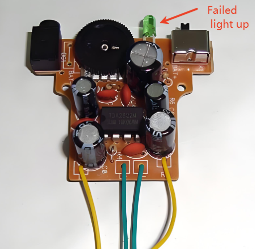
What Is LED Polarity and Why Does It Matter? LED polarity is one of the most important things to understand when working with LEDs, especilly in PCB assembly. A wrong LED polarity put will cause the failure of the PCB product. Unlike regular bulbs, LEDs only work if they are connected the right way. If you mix up the positive and negative sides, the LED won’t light up. So, whether you’re building a simple LED circuit, installing LED light strips, or working with surface-mount LEDs, understanding LED polarity helps prevent issues. In this guide, we’ll answer the most common questions about LED polarity and explain how to identify and test LED connections correctly.

What Is LED Polarity and Why Does It Matter?

What Is LED Polarity?

LED polarity refers to the direction in which an LED must be connected to a power source. Since LEDs are diodes, they allow current to flow in only one direction. This means that one leg of the LED must be connected to the positive side of the power supply, while the other must go to the negative side.

Each LED has two legs:

  • Anode (+): This is the positive leg. It needs to be connected to the positive terminal of the power source.
  • Cathode (-): This is the negative leg. It must connect to the negative terminal.

If the LED is wired incorrectly, it won’t light up because no current will flow through it. Some LEDs may even get damaged if too much voltage is applied in the wrong direction.

Do LEDs Have Polarity?

Yes, LEDs have polarity, and they must be connected correctly to function. Unlike traditional incandescent bulbs that work regardless of connection direction, LEDs only operate when the anode is connected to the positive voltage and the cathode to the ground.

The reason for this is that LEDs are light-emitting diodes. Diodes are semiconductor components that allow current to pass in one direction while blocking it in the other. When you reverse the polarity of an LED, it stops conducting electricity, which means it won’t produce light.
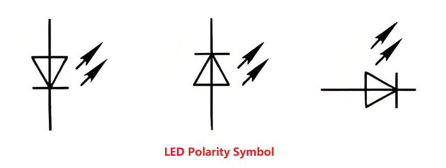
LED Polarity Symbol

If you look at circuit diagrams, you’ll notice a special symbol used for LEDs. The LED polarity symbol is similar to a regular diode symbol but has two arrows pointing away from it to indicate light emission. Below are the common led polarity symbols used in the industry:

What Is LED Polarity and Why Does It Matter?

Are LED Light Bulbs Polarity Sensitive?

It depends on the type of LED light bulb.

  • AC-powered LED bulbs (like household LED light bulbs) are usually not polarity sensitive because they contain internal rectifiers that convert AC to DC.
  • DC-powered LEDs (such as those used in automotive applications, flashlights, or indicator lights) are polarity sensitive and will not work if connected incorrectly.

When working with DC-powered LED systems, checking the wiring is crucial. Many LED strips and car LEDs have markings to indicate which side should connect to positive and which should go to negative.

How Do You Identify the Polarity of an LED?

There are several ways to determine LED polarity:

1. Check the Lead Length

If it has leds, check the lead length is the most important method to identify:

  • The longer lead is the anode (+).
  • The shorter lead is the cathode (-).
What Is LED Polarity and Why Does It Matter?

This method works well for new LEDs, but if the leads are trimmed, other methods may be needed.

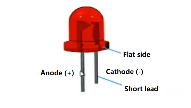
2. Look for a Flat Edge

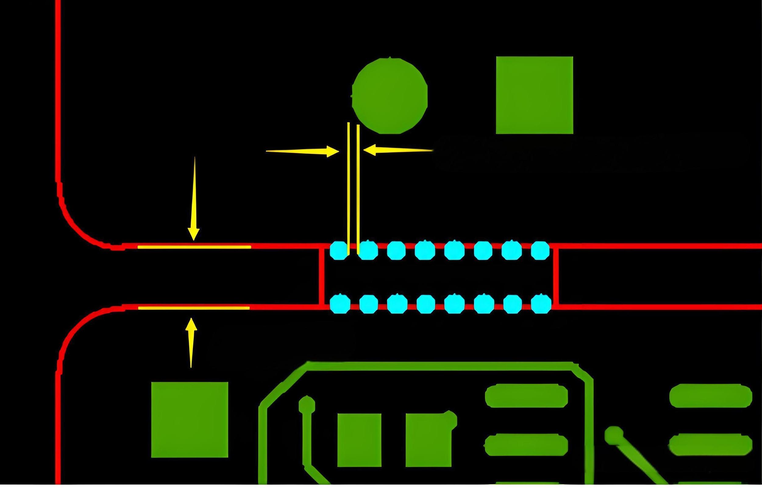
On many through-hole LEDs, the cathode side has a flat edge on the plastic casing. This marking helps quickly identify polarity. (Please refer above images of LED).

3. Inspect the Internal Structure

If you have a clear LED, you can look inside:

  • The larger internal piece is usually the cathode (-).
  • The smaller piece is the anode (+).

This method works well for transparent or diffused LEDs but is harder for small surface-mount LEDs.

4. Use a Multimeter

A digital multimeter with a diode test function can confirm polarity. When the red probe touches the anode and the black probe touches the cathode, the LED will glow slightly or show a voltage reading. If no reading appears, reverse the probes.

What Happens If LED Polarity Is Reversed?

If the LED is connected backward, it won’t light up. Unlike incandescent bulbs, which work in either direction, LEDs only allow current to flow in one way. Here are some common issues if LED polarity is reversed:

1. No Light Emission: Since LEDs are polarized components, they only work when connected correctly. If the polarity is reversed, current cannot flow, and the LED will not light up.

What Is LED Polarity and Why Does It Matter?

2. Potential Damage: In some cases, a reversed connection may cause damage. Excessive reverse voltage or current can harm the internal structure of the LED.

3. Overheating: Incorrect polarity may lead to improper current flow, generating excess heat. This can affect both the LED and nearby circuit components.

4. Short Circuit Risk: A severe polarity reversal could create a short circuit, which may harm the power source or other connected components.

5. Unstable Lighting: In rare cases, an incorrectly wired LED may flicker or dim unpredictably instead of staying off completely.

In most cases, a reversed LED will not get damaged unless the voltage is too high. However, some circuits use protection resistors or diodes to prevent issues caused by incorrect polarity.

Does LED Polarity Matter?

Yes, LED polarity matters because LEDs are diodes that function only when connected correctly. If you ignore polarity, the LED won’t work. In some cases, incorrect wiring can cause damage, especially in high-power LEDs or integrated circuits.

To avoid problems:

  • Always check the polarity markings before connecting an LED.
  • Use a multimeter if unsure.
  • Follow circuit diagrams carefully.

How to Check an LED with a Multimeter?

Using a multimeter is one of the easiest ways to test an LED’s polarity and functionality. Here’s a step-by-step guide:

1. Set the Multimeter to Diode Test Mode

Most digital multimeters have a diode test mode, usually marked with a diode symbol (a triangle pointing to a line). If your multimeter doesn’t have this mode, use the resistance (Ω) setting on the lowest range.

2. Identify the Probes

  • The red probe is the positive (+) lead.
  • The black probe is the negative (-) lead.

3. Connect the Probes to the LED Legs

Touch the red probe to one leg and the black probe to the other.

  • If the LED lights up faintly or shows a voltage reading (typically 1.8V to 3.5V, depending on the LED type), the red probe is on the anode (+), and the black probe is on the cathode (-).
  • If nothing happens, swap the probes and try again.

4. Interpret the Results

  • If the LED lights up, it means it is working, and you have identified the correct polarity.
  • If the LED doesn’t light up in either direction, it may be faulty or burned out.
  • If using the resistance mode, a working LED will show a resistance value in one direction and an infinite resistance (OL) in the other.

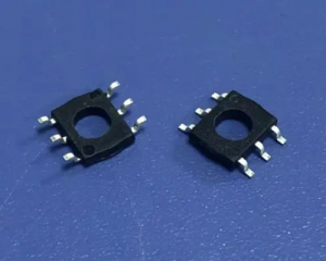
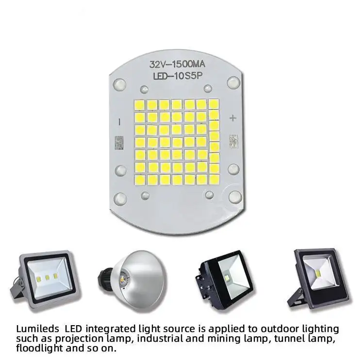
5. Testing Surface-Mount LEDs (SMD LEDs)

Since SMD LEDs are small and lack long leads, identifying polarity can be tricky. Many have a small marking on the cathode side. To test them:

  • Use fine-tip multimeter probes.
  • Hold the probes gently on the pads.
  • Observe if the LED lights up or if a voltage reading appears.

A multimeter is a quick and reliable tool to check LED polarity before installing it in a circuit.

Which Side of the LED Should You Put a Resistor?

A resistor is needed to control current flow and protect the LED. The resistor can go on either side of the LED—anode or cathode—without affecting polarity. However, placing it on the anode side (+) is common for consistency in circuit designs.

Without a resistor, the LED might receive too much current, which could shorten its lifespan or cause it to burn out.

FAQs

1. Can LED polarity be ignored?

No, LED polarity is essential for proper operation. If wired incorrectly, the LED will not work.

2. Do surface-mount LEDs have polarity?

Yes, surface-mount LEDs have polarity. Manufacturers usually mark the cathode with a dot or a line.

3. What happens if an LED is connected to AC power?

An LED without a rectifier will flicker or not work properly on AC power. A rectifier or resistor is needed for AC operation.

4. How do I fix a reversed LED?

Simply swap the connections. If the LED hasn’t been damaged, it should work fine.

5. Why do some LEDs have built-in resistors?

Built-in resistors simplify wiring by ensuring safe current levels. These LEDs can be directly connected to power sources without extra components.

You may also like

Turnkey EMS PCB Manufacturer: What Is Turnkey EMS?
Thursday, February 13th, 2025

A turnkey EMS PCB manufacturer provides a complete solution for the assembly of printed circuit boards (PCBs). From design and prototyping to final assembly, they manage the entire process. This all-in-one service is invaluable for businesses looking for efficiency and quality. But what exactly does this process entail, and why should companies opt for a turnkey approach? This article dives into the key aspects of turnkey EMS PCB manufacturing, comparing it with other options, and exploring the benefits and challenges it brings.

What is Turnkey EMS PCB Manufacturing?

Turnkey EMS PCB manufacturing refers to a comprehensive service where the manufacturer handles everything from the initial design to the final product. “Turnkey” means that the service is provided as a complete package. This typically includes designing, sourcing materials, PCB assembly, testing, and delivery.

The key advantage of turnkey EMS manufacturing is that it saves time and effort for the customer. Instead of working with multiple suppliers or manufacturers, the customer can rely on one provider for the entire process. This leads to faster timelines, better communication, and often lower costs due to streamlined operations.

What is EMS vs OEM?

It’s important to understand the difference between EMS (Electronic Manufacturing Services) and OEM (Original Equipment Manufacturer), as these terms are often used interchangeably but serve different purposes.

EMS (Electronic Manufacturing Services): A company that provides manufacturing services, including production, assembly, testing, and logistics, based on client specifications. EMS providers do not own the IP of the products they manufacture.

OEM (Original Equipment Manufacturer): A company that designs and manufactures products or components, which are then sold to another company to be branded or integrated into their products. OEMs own the intellectual property (IP) of their products.

An OEM typically designs and creates the product, and then outsources the manufacturing process to an EMS provider. While OEMs may work with EMS providers, they maintain control over the product’s design and specifications.

What Process Does Turnkey EMS PCB Manufacturing Have?

Turnkey EMS (Electronic Manufacturing Services) PCB manufacturing is a comprehensive, end-to-end solution that handles every stage of production, from design validation to final delivery. Below is the detailed process:

1. Design Review & DFM Analysis

Design Input: The client provides design files (Gerber, BOM, assembly drawings).

Design for Manufacturability (DFM): The EMS provider identifies potential production risks (e.g., pad spacing, hole sizing) and suggests optimizations to prevent costly revisions.

Prototyping (Optional): Functional prototypes are built for validation if the design isn’t finalized.

2. PCB Fabrication

Raw Board Production: Manufactures blank PCBs through processes like lamination, drilling, copper plating, etching, and solder mask application.

Quality Checks: Copper thickness verification; Impedance control (for high-frequency boards); Surface finish application (ENIG, OSP, HASL, etc.)

3. Component Sourcing & Supply Chain Management

BOM Breakdown: Segregates client-approved vendor lists (AVL) from EMS-procured components.

Risk Mitigation: Alternate component qualification (to avoid obsolescence); MOQ (Minimum Order Quantity) negotiation; Long-lead-time material stocking

4. PCB Assembly (PCBA)

SMT Assembly: Automated placement of surface-mount components (ICs, resistors, capacitors) using pick-and-place machines.

Critical steps: Solder paste printing, reflow oven profiling

Inspection: SPI (Solder Paste Inspection) and AOI (Automated Optical Inspection)

THT Assembly: Through-hole component insertion (connectors, large capacitors) using wave soldering or hand soldering.

Post-Assembly: Cleaning (flux residue removal) or conformal coating for high-reliability applications.

5. Testing & Validation

Electrical Testing: ICT (In-Circuit Test): Checks shorts, opens, and component values. FCT (Functional Test): Validates board performance under real-world conditions.

Environmental Stress Testing (as required): Thermal cycling; Vibration testing; Burn-in testing;

Compliance: Supports certifications like CE, FCC, or UL.

6. Packaging & Delivery

ESD-Safe Packaging: Anti-static bags, foam inserts, or moisture-resistant materials.

Traceability: Labels/QR codes for batch/date tracking.

Logistics: Supports JIT (Just-in-Time) delivery, drop shipping, or warehouse management.

How to Choose a PCB Manufacturer?

Choosing the right turnkey EMS PCB manufacturer is a critical decision for any business. Here are a few things to consider when selecting a manufacturer:

Experience and Reputation: Look for a manufacturer with a solid track record in the industry. A provider with years of experience and a good reputation will likely provide high-quality results.

Capabilities and Services: Ensure the manufacturer offers the full range of services you need. Check whether they provide design assistance, component sourcing, assembly, and testing, as these can save you time and money.

Quality Control Standards: A good PCB manufacturer will adhere to international quality standards. Check their certifications and quality control processes to ensure they meet industry benchmarks.

Customer Support: Good communication is key to any successful partnership. Look for a manufacturer who provides excellent customer support and is responsive to your needs.

What Benefits Can the Turnkey EMS PCB Manufacturer Bring?

The turnkey EMS PCB manufacturer offers numerous benefits that can positively impact your business:

Simplified Process: Working with a single provider reduces the complexity of coordinating between different suppliers and manufacturers.

Cost Efficiency: By consolidating services, turnkey solutions can often be more cost-effective than hiring multiple suppliers or managing different stages of production.

Faster Time-to-Market: Turnkey manufacturers can reduce lead times by streamlining the design, assembly, and testing processes. This leads to quicker product launches.

Higher Quality Assurance: Since the manufacturer handles all aspects of the production, they are in a better position to ensure consistency and quality throughout the process.

These benefits make turnkey EMS PCB manufacturing an appealing option for companies aiming for streamlined operations and reliable results.

What Are the Key Challenges of Working with a Turnkey EMS PCB Manufacturer?

‌The key challenges of working with a turnkey EMS (Electronic Manufacturing Services) PCB manufacturer, from a positive perspective, include ensuring effective communication, managing expectations, and maintaining quality control.‌

‌Ensuring Effective Communication‌: Collaboration with a turnkey EMS PCB manufacturer often involves detailed technical specifications and ongoing adjustments. Ensuring clear and timely communication is crucial to avoid misunderstandings that could lead to delays or product defects.

‌Managing Expectations‌: Both parties need to have realistic expectations about timelines, costs, and the scope of work. Managing these expectations effectively can prevent scope creep and ensure that the project stays on track.

‌Maintaining Quality Control‌: Maintaining high standards of quality control is essential when outsourcing PCB manufacturing. This involves setting clear quality benchmarks, conducting regular audits, and having a robust system in place to address any quality issues promptly.

By addressing these challenges proactively, companies can leverage the benefits of working with a turnkey EMS PCB manufacturer, such as cost savings, access to advanced manufacturing capabilities, and faster time-to-market‌.

How to Ensure Quality Control with a Turnkey EMS PCB Manufacturer?

Quality control is crucial in PCB manufacturing, and a good turnkey EMS PCB manufacturer should have stringent quality control measures in place. Here’s how to ensure quality:

Clear Specifications: Provide the manufacturer with detailed design and performance specifications. This helps minimize mistakes and ensures that the product meets your exact needs.

Regular Testing: Ensure the manufacturer conducts regular testing throughout the process, including before, during, and after assembly. This should include electrical testing and reliability tests.

Third-Party Audits: Consider having third-party audits or inspections done to verify the quality and compliance of the final product. This adds an extra layer of confidence in the manufacturer’s processes.

By ensuring a strong quality control process, you can reduce the risk of defects and ensure that your PCBs meet industry standards.

At Best Technology, we are committed to delivering top-tier turnkey EMS PCB manufacturing services. Our comprehensive approach combines expert design, precise component sourcing, and meticulous testing to ensure your PCBs meet the highest standards. With a focus on quality, efficiency, and customer satisfaction, we take pride in being a trusted partner for companies looking for seamless, reliable PCB solutions.

To put it in a nutshell, a turnkey EMS PCB manufacturer offers significant advantages for businesses looking to streamline their PCB manufacturing process. From design and assembly to testing and delivery, they manage it all, saving you time and effort. While there are some challenges, such as Complexity in Communication, Quality Control, the benefits often outweigh the drawbacks. By carefully selecting a reputable provider and ensuring effective communication, you can enjoy a seamless manufacturing experience with high-quality results.

If you’re looking for a reliable and efficient PCB manufacturing partner, a turnkey EMS solution might just be what you need. Best Technology is a leading turnkey EMS PCB manufacturer with years of experience in providing high-quality, reliable PCB solutions. Our expertise in the industry ensures that our clients receive the best possible solutions tailored to their specific needs, all while maintaining the highest standards of quality and efficiency. Pls feel free to contact us at sales@bestpcbs.com to get more information and personalized solutions.

You may also like

What is the smt meaning? SMT meaning manufacturing
Wednesday, February 12th, 2025

What is the smt meaning? SMT, or Surface Mount Technology, is an advanced manufacturing process that directly mounts electronic components on the surface of a printed circuit board (PCB). It replaces the traditional through-hole insertion technology with an efficient and precise automated production method, and achieves miniaturization and high-density integration of electronic components.

What is the smt meaning? SMT meaning manufacturing

What does smt mean?

SMT stands for Surface Mount Technology, a revolutionary approach to assembling electronic circuits. Instead of using traditional through-hole components, where pins pass through drilled holes, SMT enables components to be directly mounted onto the surface of a PCB.

This advancement has led to more compact and lightweight electronic devices, transforming industries such as consumer electronics, automotive, medical, and aerospace. By eliminating the need for large holes and complex routing, SMT increases design flexibility and enhances overall performance.

What does SMD and SMT stand for?

  • SMD (Surface Mount Device): These are electronic components specifically designed for surface mounting. They are smaller than through-hole components and have no long leads, allowing for denser and more complex PCB layouts.
  • SMT (Surface Mount Technology): This refers to the entire process of placing, soldering, and inspecting SMDs on a PCB. SMT is now the standard in electronics manufacturing, replacing traditional methods due to its superior efficiency, cost-effectiveness, and capability to handle high-density designs.

What are the different types of SMT?

SMT technology encompasses various component types and mounting techniques. The main types include:

  • Passive Components: Small resistors, capacitors, and inductors designed to be surface-mounted, helping regulate voltage and current flow.
  • Active Components: Transistors, diodes, and integrated circuits that drive processing and logic functions in electronic devices.
  • Fine-Pitch Components: Used in high-performance applications, these components have closely spaced terminals that require precision soldering.
What is the smt meaning? SMT meaning manufacturing
  • Ball Grid Array (BGA): A package type where solder balls are placed under the component, offering improved thermal performance and electrical connections.
  • Chip-Scale Packages (CSP): Miniature packages designed to be nearly the same size as the silicon chip itself, essential for mobile and compact devices.
  • Quad Flat Package (QFP): Integrated circuits with leads extending from four sides, commonly used in microcontrollers and processors.

What are the features of SMT?

SMT offers numerous advantages that have made it the preferred technology in PCB assembly:

  • Compact Design: SMT components are much smaller than their through-hole counterparts, allowing for lightweight and space-saving designs.
  • Higher Component Density: With no need for drilled holes, more components can fit within a given board area, increasing functionality.
  • Improved Electrical Performance: Shorter electrical paths minimize resistance and inductance, enhancing signal transmission speed and reducing power loss.
  • Automated Assembly: SMT allows for high-speed, automated component placement, reducing human error and increasing production efficiency.
  • Lower Manufacturing Costs: Reduced material waste, automated processing, and high production throughput lead to significant cost savings.
  • Better Thermal Management: SMT designs allow for better heat dissipation, which is crucial for high-power applications.
  • Stronger Mechanical Performance: Components mounted using SMT are more resistant to vibrations and mechanical stress, making them ideal for aerospace and automotive industries.

Why is SMT used?

The widespread adoption of SMT stems from its numerous benefits in electronics manufacturing. Companies prefer SMT because:

  • It enables miniaturization: Modern electronic devices require compact and lightweight designs, which SMT facilitates.
What is the smt meaning? SMT meaning manufacturing
  • It enhances production speed: Automated SMT assembly lines can place thousands of components per hour, boosting manufacturing efficiency.
  • It improves product reliability: Stronger mechanical connections and reduced solder joint defects lead to more durable and long-lasting products.
  • It reduces manufacturing costs: Automated SMT processes lower labor costs while increasing yield rates.
  • It supports high-performance applications: SMT minimizes electrical noise, making it suitable for fast processors, 5G technology, and other advanced applications.

What are the processes of SMT?

The SMT assembly process consists of multiple steps, each requiring precision and expertise to ensure high-quality PCB production:

  • PCB Preparation: The bare PCB is cleaned to remove contaminants and treated with coatings to prevent oxidation and improve solder adhesion.
  • Solder Paste Application: Solder paste, a mixture of flux and metal particles, is applied to PCB pads using stencils or jet printing, ensuring precise placement.
  • Component Placement: Automated pick-and-place machines position SMDs onto the solder-pasted PCB with extreme accuracy, ensuring proper alignment.
  • Reflow Soldering: The assembled PCB is passed through a controlled heating process, where the solder paste melts and forms strong electrical connections.
  • Inspection and Quality Control: Techniques such as Automated Optical Inspection (AOI) and X-ray testing detect defects like misalignment, solder bridging, and voids.
  • Final Cleaning and Packaging: Flux residues are removed, and the PCBs are tested and packaged for delivery to clients.
  • Functional Testing: Completed PCBs undergo rigorous functional tests to verify performance and compliance with industry standards.

What is SMT and THT?

Two primary methods exist in PCB assembly: Surface Mount Technology (SMT) and Through-Hole Technology (THT). While SMT has largely replaced THT, both technologies serve specific applications.

Key Differences:

  • Size & Weight: SMT components are smaller and allow for lighter devices, whereas THT components are larger and bulkier.
What is the smt meaning? SMT meaning manufacturing
  • Assembly Efficiency: SMT supports automation, enabling fast and precise production, while THT often requires manual assembly, making it slower.
  • Application Suitability: SMT is preferred for consumer electronics, telecommunications, and medical devices, whereas THT is used in military, aerospace, and high-power applications.
  • Reliability: SMT offers excellent electrical performance, while THT provides stronger mechanical bonds for applications exposed to extreme stress.

Conclusion:

Surface Mount Technology has revolutionized modern electronics, making devices smaller, more powerful, and cost-efficient. With its high-speed production, improved electrical performance, and ability to support complex designs, SMT has become the industry standard.

For high-quality SMT PCB solutions, reach out to Best Technology at sales@bestpcbs.com

You may also like

What is an assembly PCB? & PCB Fabrication Manufacturer
Thursday, January 9th, 2025

What is an Assembly PCB? Assembling PCB refers to the process of installing electronic components on a printed circuit board. Through this process, various electronic components such as resistors, capacitors, chips, etc. are fixed on the PCB through welding technology to form a complete electronic circuit.

Assembling PCB is a key step in the manufacture of electronic equipment, which enables electronic components to be connected according to the designed circuit to achieve the functions and performance of electronic equipment.

What is an assembly PCB? & PCB Fabrication Manufacturer

What is the PCB Assembly Process?

PCB assembly is the process of attaching electronic components to a printed circuit board (PCB) to create a working electronic circuit.  The primary goal is to ensure that all parts of the circuit are correctly connected and able to transmit electrical signals.

The PCB assembly process mainly includes the following steps:

  • Solder paste printing: First, print the solder paste on the PCB, which is done by using a template to accurately apply the solder paste to the pads of the PCB.
  • Component placement: Use a high-speed, high-precision placement machine to place the components on the PCB. The placement machine accurately places the components at the predetermined position based on the coordinate information in the design file.
What is an assembly PCB? & PCB Fabrication Manufacturer
  • Soldering: After the component placement is completed, the soldering process is carried out. For surface mount components, reflow soldering is usually used, and the PCB is sent into the reflow soldering oven, and the solder paste is melted by heating, so that the components are soldered to the PCB. For through-hole components, wave soldering is used.
  • Inspection and testing: After the soldering is completed, inspection and testing are carried out to ensure the assembly quality. Automated optical inspection (AOI) equipment is usually used to check the soldering quality and the accuracy of component placement.
  • Rework and packaging: For defective products found during the inspection, rework is carried out. Qualified PCB assembly boards are packaged for transportation and storage.

The entire PCB assembly process requires a high degree of automation and precise control to ensure the quality and reliability of the final product.

What is the Standard for PCB Assembly?

The standard for PCB assembly depends on several industry-specific certifications and guidelines. However, some of the most widely recognized standards include:

  • IPC-2221: This standard provides the generic requirements for designing and manufacturing PCBs, including assembly considerations.
  • IPC-A-610: Often referred to as the “Acceptability of Electronic Assemblies,” this standard covers the acceptability criteria for soldering, component placement, and the quality of assembly in general.
  • ISO 9001: Many PCB assembly manufacturers are certified to this standard, which ensures that they follow consistent quality management practices in their processes.

These standards help ensure that the PCB assembly process is carried out in a controlled and quality-assured manner.

What Files are Needed for PCB Assembly?

A successful PCB assembly requires the right files to communicate the design and specifications to the manufacturer. Some of the essential files include:

  • Gerber Files: These files provide the detailed design of the PCB, including copper traces, pads, and other essential information for PCB fabrication.
  • Bill of Materials (BOM): The BOM lists all the components that will be used in the assembly, such as resistors, capacitors, and ICs.
What is an assembly PCB? & PCB Fabrication Manufacturer
  • Pick-and-Place Files: These files contain the specific information about where each component will be placed on the PCB, which is essential for automated placement machines.
  • Stencil File: This file is used for creating the solder paste stencil, which is used to apply solder paste to the PCB during the soldering process.

These files ensure that the PCB board assembly is accurate and matches the original design specifications.

What Are the Materials Used in PCB Assembly?

The materials used in PCB board assembly are crucial to the functionality and performance of the finished product. Some of the most commonly used materials include:

  • PCB Substrate: The most common material is FR4 (fiberglass resin), but for high-performance applications, materials like aluminum or ceramic may be used.
  • Solder Paste: A mixture of metal solder and flux, solder paste is used to attach components to the PCB during the soldering process.
  • Soldering Materials: Lead-based or lead-free solder is used to create permanent connections between the PCB and components.
  • Components: Resistors, capacitors, ICs, and other components are soldered onto the PCB. These can be sourced from various manufacturers and come in a variety of shapes and sizes.

Each material is selected based on the needs of the specific application. For example, ceramic PCBs are chosen for high-temperature environments, while aluminum-backed PCBs are selected for heat dissipation.

What is the Difference Between PCB Fabrication and PCB Assembly?

Many people confuse PCB fabrication with PCB assembly, but the two are distinct steps in the PCB manufacturing process.

PCB Fabrication refers to the process of creating the physical PCB from raw materials. This includes the creation of the PCB’s layers, the copper traces, drilling holes for vias, and etching the patterns that connect the components. In simple terms, PCB fabrication is the creation of the “bare” board.

PCB Assembly, on the other hand, refers to the process of attaching electronic components to the fabricated PCB. This involves placing and soldering the components to form a functional circuit.

So, PCB fabrication is all about making the PCB, and PCB assembly is about making it functional by adding components.

What is the Difference Between SMD and SMT in PCB?

The terms SMD (Surface-Mounted Device) and SMT (Surface-Mount Technology) are often used interchangeably, but they refer to different aspects of the assembly process.

SMD refers to the actual components used in the assembly process. These components are designed to be mounted directly onto the surface of the PCB rather than through-hole components, which are inserted into holes drilled into the board.

What is an assembly PCB? & PCB Fabrication Manufacturer

SMT, on the other hand, refers to the technology and process used to assemble SMDs onto the PCB. SMT involves automated machines that place components onto the PCB and then solder them into place, typically using reflow soldering.

In summary, SMD refers to the components, and SMT refers to the method of attaching those components.

Conclusion

PCB assembly is a critical step in creating functional electronic circuits. From the placement of components to the soldering process and final testing, every aspect of assembly must be carefully executed to ensure a reliable and high-performance product. If you have any PCB assembly needs, feel free to contact BEST Technology at sales@bestpcbs.com.

You may also like

Why You Need Turnkey PCBA Assembly Service Right Now?
Thursday, January 9th, 2025

Turnkey PCBA assembly service has become an essential part of the manufacturing industry, particularly in electronics. It provides a complete solution for companies needing printed circuit board assemblies (PCBAs) but lacking the resources or expertise to handle the intricate process themselves.

What is Turnkey PCB Assembly?

Turnkey PCB assembly is a full-service solution for the production of printed circuit boards (PCBs) and their assembly into functional electronic products. This service includes everything from designing the circuit boards to sourcing the components, assembling the PCBs, and delivering the final product. The term “turnkey” refers to a ready-to-use product, where you simply provide the specifications, and the service provider takes care of the rest.

In a typical turnkey PCBA assembly service, the manufacturer handles every step in the process, ensuring that the product meets the client’s requirements without the need for them to get involved in the details. This eliminates the need for multiple suppliers, reducing costs and saving time.

What Does Turnkey Mean in Manufacturing?

In manufacturing, turnkey refers to a complete solution where the service provider is responsible for every aspect of production. This includes design, sourcing materials, manufacturing, and testing. Once the project is completed, the product is ready for immediate use, hence the term “turnkey.” It offers simplicity for clients, as they can rely on a single supplier for all their manufacturing needs.

For PCB assembly, this means that the manufacturer will take care of everything from sourcing the necessary components to assembling and testing the final product. The client’s only responsibility is to supply the initial design or specification.

What is the Difference Between PCB and PCB Assembly?

A PCB (Printed Circuit Board) is a flat, rigid board used to mechanically support and electrically connect electronic components. It serves as the base for the circuit components that make up an electronic device, such as resistors, capacitors, and chips. The PCB itself does not perform any function until components are attached.

PCB assembly, on the other hand, refers to the process of placing and soldering these electronic components onto the PCB. The result is a complete, functional assembly, often called a PCBA (Printed Circuit Board Assembly). The assembly process involves precise placement, soldering, and testing of components to ensure the board works as intended.

What Specific Services Are Included in Turnkey PCBA Assembly Service?

A turnkey PCBA assembly service typically includes the following services:

1. PCB Design: If you don’t have a design yet, some providers offer PCB design services, creating the layout and schematic based on your specifications.

2. Component Sourcing: This includes purchasing all the components necessary for your project, ensuring they meet the required standards.

3. PCB Manufacturing: This is the process of producing the actual PCB, including layer stacking, etching, drilling, and other steps to create the board itself.

4. PCB Assembly: The components are placed on the PCB and soldered into place, often using automated machines for precision.

5. Testing and Inspection: Quality checks such as functional testing, X-ray inspection, and visual inspection ensure that the PCB is properly assembled and functional.

6. Packaging and Delivery: The final product is packaged and shipped to the client, ready for integration into the final product.

This comprehensive approach reduces lead times and ensures that clients receive a finished product that meets their expectations.

What is the Major Difference Between a Turnkey Project and a Design Build?

The primary difference between a turnkey project and a design build lies in the scope of responsibility.

Turnkey Projects: In a turnkey project, the service provider is responsible for every aspect of the project, from start to finish. The client hands over the specifications, and the provider handles design, procurement, manufacturing, and testing. Once completed, the product is ready for use.

Design Build Projects: In a design-build project, the client has more involvement. The service provider is typically responsible for the design and construction, but the client may still need to source components or provide additional input during the process. The client may need to manage more aspects of the project compared to a turnkey approach.

While both models aim to streamline production, turnkey projects are more hands-off for the client and typically offer greater convenience and efficiency.

What Files Are Needed for PCB Assembly?

To begin the PCB assembly process, several files are necessary. These files provide the information needed for manufacturing and assembling the PCB:

1. Gerber Files: These are the standard files for PCB design and detail the layers of the PCB, including copper layers, silkscreen layers, and soldermask layers.

2. Bill of Materials (BOM): A list of all the components required for the PCB assembly, including their specifications and quantities.

3. Pick-and-Place Files: These files contain precise information about where each component should be placed on the PCB, ensuring accurate placement during assembly.

4. Assembly Drawings: These drawings provide a visual reference for the assembly process, often showing where components should be placed.

5. Test Specifications: Details about the tests that need to be performed on the finished PCB to ensure quality and functionality.

These files ensure that every aspect of the production process is well-defined and can be accurately followed.

How Does PCB Assembly Work?

The PCB assembly process is a multi-step procedure that involves placing and soldering electronic components onto the PCB. The basic steps are as follows:

1. Component Sourcing: The required components are sourced and inspected for quality.

2. Solder Paste Application: Solder paste is applied to the PCB in areas where components will be placed.

3. Pick-and-Place: Using automated machines, components are placed precisely on the PCB.

4. Soldering: The PCB passes through a reflow oven, where the solder paste is melted and bonds the components to the board.

5. Inspection and Testing: The assembled PCB is inspected for errors and tested to ensure functionality.

6. Final Assembly: After testing, the board is packaged and shipped to the client.

Each step requires precision and attention to detail to ensure that the final product is functional and reliable.

What Are the Advantages of Turnkey Projects?

Turnkey projects offer several advantages that make them highly attractive, especially for businesses that want a hassle-free solution:

1. Simplified Process: The client only needs to provide initial specifications, with no need to worry about the intricacies of the manufacturing process.

2. Cost Efficiency: By bundling all services under one provider, turnkey solutions often result in lower costs, especially in terms of supply chain management and reduced overhead.

3. Time Savings: The provider handles all aspects of production, resulting in faster project timelines.

4. Quality Assurance: With a single provider responsible for all phases of production, consistency and quality are easier to maintain.

5. Focus on Core Competencies: Clients can focus on their product’s design and marketing while leaving the manufacturing details to the experts.

In short, turnkey PCBA assembly services offer a seamless, efficient, and reliable way to get your PCBs assembled and ready for integration into your electronic products.

Turnkey PCBA assembly services provide a comprehensive solution that simplifies the process of getting your PCBs designed, assembled, and ready for use. With services ranging from component sourcing to final delivery, it offers businesses a one-stop shop for all their assembly needs. By choosing a turnkey provider, companies can enjoy cost savings, faster timelines, and a hassle-free manufacturing experience. Best Technology provides turnkey PCBA assembly service, delivering high-quality products with quick turnaround times. If you’re interested in our turnkey PCBA assembly service, feel free to contact us at sales@bestpcbs.com for more information.

You may also like

PCB Multilayer Circuit Board: pcb panel v-cut vs stamp hole
Tuesday, January 7th, 2025

V-CUT cuts a V-shaped groove on the PCB board, so that the board can be easily separated in subsequent processing, while the stamp hole sets a small hole on the edge of the board, making the board more neat and stable when separated, which can provide higher space utilization and better signal transmission performance. The combination of these two technologies not only improves production efficiency, but also ensures product quality and reliability.

PCB Multilayer Circuit Board: pcb panel v-cut vs stamp hole

What is PCB V-CUT?

PCB V-CUT is a technology that cuts a V-shaped groove on a printed circuit board, which is mainly used to facilitate subsequent board separation operations. V-CUT is to cut a series of V-shaped cuts on the PCB board and then break the board after applying appropriate force, thereby dividing the multilayer PCB into separate panels.

The role and importance of V-CUT

  • Improve manufacturing efficiency: In mass production, V-CUT can quickly divide large boards into multiple small panels to meet the needs of mass production.
  • Reduce material waste: Through V-CUT cutting, raw materials can be maximized, waste generation can be reduced, and production costs can be reduced.
  • Convenient assembly: V-CUT allows the separated small panels to be easily assembled and welded, improving production efficiency.

V-Cut is widely used in the batch manufacturing of multi-layer PCBs, especially when a large board needs to be divided into multiple small panels.

What are the advantages and disadvantages of V-Cut?

Advantages of V-Cut:

  • Easy to operate: The V-Cut design can facilitate the separation of SMT circuit boards after assembly, avoiding PCB bending and damage to electronic components that may be caused by manual separation.
  • Improve production efficiency: When assembling the edges of two boards, the efficiency of SMT patch lines and wave soldering can be significantly improved.
  • Wide range of applications: V-Cut is suitable for regular PCB boards, especially in batch production, the use of V-Cut can significantly improve production efficiency.

Disadvantages of V-Cut:

  • Can only cut straight lines: V-Cut can only cut straight lines, and it can only cut straight lines from one end to the end, and cannot be changed in the middle. If there is a 90-degree or other angle bend in the middle, it is not allowed.
PCB Multilayer Circuit Board: pcb panel v-cut vs stamp hole
  • High requirements for tools: The material and manufacturing process of V-Cut knives have a great influence on the cutting effect. For example, high-speed tool steel V-Cut knives are not wear-resistant and need to be frequently changed and sharpened, which affects production efficiency; alloy-inlaid V-Cut knives increase the brittleness of the blade due to welding, and the quality is difficult to guarantee, and the tooth breakage rate is high.
  • Restrictions on PCB thickness: PCB boards that are too thin or too thick are not suitable for V-Cut, because too thin boards are easy to break and too thick boards are difficult to cut.

What is a stamp hole?

A stamp hole refers to a hole on the motherboard panel that is used to connect small PCBs that make up the array together and to easily remove components from the PCB. Stamp holes are perforated, and when pushed down, the holes break, allowing components to be removed without damaging the PCB itself.

The specific functions of stamp holes include:

  • Connecting small PCB boards: When there are multiple small PCBs that need to be connected and connectors cannot be used, they can be connected through stamp holes. Perforations allow current to flow through the PCB and connect with other nearby PCBs.
  • Transmit power and data: Stamp holes can transmit power and data between two different PCBs or devices to achieve communication between devices.

Design requirements for stamp holes include:

  • Number of holes: Usually stamp holes are in groups of 5 to connect components together, but the specific number may vary depending on the PCB design.
PCB Multilayer Circuit Board: pcb panel v-cut vs stamp hole
  • Size: The size of stamp holes is usually 0.020 inches or 0.5 mm in diameter, and the specific size will vary depending on the PCB design.
  • Hole spacing: The spacing of stamp holes is usually 0.030 inches or 0.76 mm to prevent components from being too close and causing short circuits.

In addition, design tips for stamp holes include:

  • Sufficient pull tabs: In order to maintain the integrity of the PCB, the pull tabs should be strong enough to support the weight of the components above.
  • Stay away from sensitive components: Stamp holes should be away from sensitive components to avoid electrical short circuits caused by damage to the pull tabs.
  • Spacing: The spacing between two stamp holes should be between 60mm-90mm to facilitate the installation of components.

What are the advantages and disadvantages of stamp holes?

The advantages of stamp holes include:

  • Improved production efficiency: Stamp holes can connect multiple small-sized PCBs together for production and processing, thereby simplifying the production process and reducing costs.
  • Convenient assembly and disassembly: In situations where detachable connections are required, such as modular designs, stamp hole connections can achieve convenient assembly and disassembly, facilitating product repair and upgrades.
  • Reduced space occupation: The stamp hole design can greatly reduce the required space, especially suitable for compact designs.
  • Improved signal transmission performance: Stamp holes shorten the signal path, reduce signal delay and cross interference, and are suitable for complex multi-layer board designs.
PCB Multilayer Circuit Board: pcb panel v-cut vs stamp hole

Disadvantages of stamp holes include:

  • Possible cost increase: The design of stamp holes will increase certain costs because holes need to be reserved on the PCB, and the size of these holes will also be included in the overall size of the PCB.
  • The broken surface is not easy to control: Stamp holes are separated by breaking, and the broken surface is not easy to control accurately, which may cause line damage or even scrap.

What is the difference between V-Cut and stamp hole?

The main difference between V-Cut and stamp hole lies in their definition, purpose and applicable scenarios.

  • V-Cut: V-Cut is to pre-cut a V-shaped dividing line at a specific position of the PCB, which is usually used to facilitate the de-paneling (De-paneling) of the SMT circuit board after assembly. The dividing line of V-Cut is generally a straight line, without complex curves or arcs, and is suitable for panel connection of conventional PCB boards.
  • Stamp hole: Stamp hole is to connect the process edge and the PCB board by punching a series of circular holes shaped like stamps on the PCB board. It is mainly used for irregular shaped PCB boards, such as circles. Since V-Cut cannot achieve this connection, stamp holes are more used in special-shaped boards.

How to choose a suitable PCB de-paneling method?

Choosing a suitable PCB de-paneling method requires considering multiple factors, including the shape of the PCB, the scale of production, the cost budget, and the requirements for product quality.

1. V-CUT (V-shaped cutting):

  • Advantages: low cost, simple operation, fast speed, suitable for regular shaped PCBs arranged in a straight line.
PCB Multilayer Circuit Board: pcb panel v-cut vs stamp hole
  • Disadvantages: only straight line de-paneling can be performed, which is not suitable for complex or irregular shaped PCBs.
  • Applicable scenarios: suitable for small and medium batch production, and the PCB shape is relatively regular.

2. Stamp hole:

  • Advantages: Suitable for irregular shaped PCBs, such as round or special-shaped boards, and can provide better space utilization.
  • Disadvantages: Compared with V-CUT, the cost is slightly higher, and some burrs may be generated during the separation process.
  • Applicable scenarios: Suitable for PCBs with complex or irregular shapes, and production that requires high space utilization.

3. Milling cutter type board separation:

  • Advantages: It can be divided into boards of any shape, with smooth cutting edges and low stress, and is suitable for PCBs of various shapes.
  • Disadvantages: The initial cost is high, and the equipment and operation are relatively complex.
  • Applicable scenarios: Suitable for complex-shaped PCBs with high cutting accuracy requirements.

4. Laser board separation:

  • Advantages: High precision, suitable for PCBs with complex shapes and high precision requirements.
  • Disadvantages: High cost and slow speed.
  • Applicable scenarios: Suitable for small-batch production with high precision requirements.

When choosing a board separation method, factors such as the specific needs of the product, production costs, production efficiency, and requirements for product quality should be comprehensively considered to ensure that the most appropriate board separation method is selected.

In summary, both have their own advantages and disadvantages. V-CUT is particularly suitable for regular-shaped PCB boards with its low cost and high efficiency, while stamp holes show unique advantages when dealing with irregular-shaped boards or boards that require higher space utilization. We need to choose the most suitable PCB depaneling solution according to the actual situation.

BEST Techbology has rich experience and advanced equipment, and can flexibly apply a variety of depaneling technologies such as V-CUT and stamp holes to meet the needs of different customers. Whether your PCB design is regular or complex, please feel free to contact us at sales@bestpcbs.com to get the best solution.

You may also like

What is pcb board assembly? PCB assembly manufacturer
Thursday, January 2nd, 2025

What is pcb board assembly? PCB board assembly is the process of installing various electronic components (such as resistors, capacitors, chips, etc.) on the PCB and achieving electrical connections through welding and other methods to build a circuit board that can achieve specific electronic functions. This process includes component preparation, PCB board pretreatment, welding and post-assembly inspection.

What is the assembly of a PCB?

What is pcb board assembly? PCB assembly manufacturer

PCB assembly is the process of installing and electrically connecting various electronic components to a printed circuit board according to design requirements. It includes component preparation (purchase inspection, classified storage), PCB preparation (inspection, cleaning), welding (plug-in welding and patch welding) and post-assembly inspection (appearance and electrical performance inspection). Its quality is crucial to the performance and reliability of electronic products and is widely used in consumer electronics, industrial control, communications, automotive electronics and other fields.

How do you assemble a PCB board?

  • Component preparation: Purchase electronic components according to design documents and check whether the component specifications, models and appearance are qualified. After that, the qualified components are classified and stored by type, packaging form, etc.
  • PCB preparation: Check the appearance of the PCB board for scratches, short circuits and other defects, and wipe it with a special cleaner or alcohol to ensure that the surface is free of oil and dust, and that the pads are flat and free of oxidation.
  • Soldering process: Insert the component pins into the corresponding holes of the PCB, use an electric soldering iron to melt the solder to fill the pins and pads to form solder joints, and pay attention to controlling the temperature and time.
  • SMT soldering: Print solder paste on the PCB pads, place the components with a SMT machine, and then heat them according to the temperature curve through a reflow oven to melt the solder paste to form solder joints.
  • Post-assembly inspection: Perform an appearance inspection to check the solder joints and component installation. Then perform an electrical performance test, use professional equipment to check whether the function is normal, and troubleshoot and repair the faults.

What is the function of PCB assembly?

The main functions of PCB assembly include the following aspects:

  • Electrical connection: The copper wire tracks on the PCB board can connect various electronic components (such as resistors, capacitors, and integrated circuits) to form a complete circuit system. This efficient connection method simplifies circuit design and improves circuit reliability.
  • Component support: PCB provides stable support for components. Through welding and other methods, components can be firmly mounted on PCB, which improves the structural integrity and portability of the equipment.
What is pcb board assembly? PCB assembly manufacturer
  • Circuit protection: The insulating material of PCB can effectively isolate electromagnetic interference and protect the circuit from the external environment (such as moisture, dust, etc.), thereby extending the service life of electronic equipment, especially in harsh industrial environments.
  • Heat dissipation function: In high-performance, high-power electronic equipment, the metal layer (such as copper foil) on the PCB can quickly absorb and disperse the heat generated when the circuit is working, preventing components from being damaged by overheating. By optimizing the design, such as increasing the thickness and layout of the copper foil, the heat dissipation efficiency can be further improved.
  • Space optimization and compact structure: The design of the PCB is not only related to the functional realization of the circuit, but also affects the production cost, production efficiency and subsequent maintenance and replacement. Optimizing the use of space makes the internal structure of electronic equipment more compact and beautiful.

What is the standard for PCB assembly?

The standardization of PCB assembly is one of the important measures to ensure product quality and reliability. The following are the main standards for PCB assembly:

  • PCB board size and positioning: The size and positioning of the PCB board should meet the design requirements to ensure accurate alignment and fixation during the assembly process.
  • Component welding quality: The quality of the welding point is the key. The welding point should be smooth, firm, and burr-free to avoid poor welding, cold welding and other undesirable phenomena.
  • Component arrangement and layout: The arrangement and layout of the components should meet the design requirements to ensure the correct spacing and position between the components to avoid mutual interference.
  • Solder point quality: The solder joint should be firm, smooth, and burr-free to ensure the normal operation of the circuit.
  • Appearance quality: The surface of the PCB board should be clean, flat, and scratch-free, and the components should be arranged neatly and beautifully.
  • Electrical performance: Ensure that the electrical performance of the PCB after assembly meets the design requirements.
  • Weather resistance: PCB assembly should have good weather resistance and be able to work stably under different environmental conditions.
  • Reliability: The durability and reliability of the components should be considered during the assembly process to ensure stability in long-term use.

In addition, the specific assembly standards may vary depending on different application scenarios and product types. During the assembly process, relevant standards and requirements should be followed to ensure the quality and stability of the assembly.

What files are needed for PCB assembly?

The following main files are needed in the PCB assembly process:

  • Gerber file: This is the most critical file in PCB production, which contains the geometric information of each layer of the circuit board, such as copper lines, pads, solder mask and silk screen layers. Gerber files are usually generated by CAD software and saved in a standard format.
  • Drill file (.drl or .xin): This file provides the location and size information of all the drill holes on the circuit board, ensuring that the drill holes are accurately aligned with the circuit pattern.
  • Bill of Materials (BOM): The BOM lists all the materials and components that make up the circuit board, including their quantity, specifications and supplier information.
  • Coordinate files: These files provide the coordinate and orientation information of each component on the circuit board, which is essential for the automated assembly process.
  • Assembly drawings: If the PCB needs to be assembled with other electronic components, it is necessary to provide assembly drawings or assembly instructions, which detail how the components are installed on the circuit board.
  • Test requirements: If the manufacturer is required to perform specific tests, such as functional tests or electrical performance tests, it is necessary to provide test requirements or test instructions files.
  • Design Rule Check File (DRC): Used to verify whether the PCB design meets the manufacturing requirements and standards, helping to find and correct potential problems during the design stage.
  • 3D Model (STEP File): Used to generate a 3D model of the circuit board to help simulate and verify during the production process.
  • Structure Drawing (DXF format): Used to make a CAD structure drawing of the circuit board to ensure accuracy during the manufacturing process.

When providing these files, make sure they are up-to-date, accurate, and match the production requirements. It is also very important to maintain communication with the manufacturer to ensure that they have a clear understanding of the design requirements and can produce as expected.

What are the materials used in PCB assembly?

PCB assembly mainly uses the following materials:

1. Electronic components

  • Passive components: including resistors (used to control current and voltage, with a variety of resistance values, powers and packaging forms), capacitors (used to store charge and filter, there are ceramic, electrolytic, tantalum capacitors and other types, with different capacities and withstand voltage values), inductors (used to store magnetic field energy, with winding and stacked inductors, and the unit of inductance is Henry).
What is pcb board assembly? PCB assembly manufacturer
  • Active components: such as integrated circuits (including various functional circuits, with DIP, SOP, BGA and other packaging forms), transistors (used for amplification and switching functions, with BJT and FET and other types, with different parameters).

2. Welding materials

  • Solder wire: The main component is tin-lead or lead-free alloy, with different diameters, lead-containing solder wire has a lower melting point, lead-free solder wire has a higher melting point, and often contains flux inside.
  • Solder paste: used for SMT welding, it is a mixture of solder powder and flux, and its viscosity and metal content affect the quality of printing and welding.
  • Flux: used to remove metal surface oxides and reduce solder surface tension, available in liquid, paste and other forms, and ingredients include organic acids, rosin, etc.

3. PCB substrate materials

  • FR-4: Commonly used epoxy glass fiber cloth laminate, with good insulation, mechanical strength and thermal stability, and different thicknesses.
  • Ceramic substrate: excellent thermal conductivity and high-frequency performance, such as aluminum nitride and alumina ceramic substrates, suitable for high-power and high-frequency devices.
  • Flexible PCB substrate: used for bendable or foldable devices, the material is soft, and polyimide is often used as an insulating layer.

4. Other auxiliary materials

  • Cleaning agent: used to clean impurities on PCB boards, including alcohol and special electronic cleaning agents.
  • Thermal conductive materials: such as thermal grease and thermal conductive tape, used for heat dissipation of high-power components.

How is a PCB board structured?

The basic structure of a PCB board includes multiple layers, each of which has its specific functions and effects.

PCB boards are mainly composed of the following layers:

  • Top Layer: This is the top layer of the PCB board, which is usually filled with electronic components such as resistors, capacitors, and chips. The top layer not only carries these components, but also is responsible for their connection and wiring to ensure that current and signals can be accurately transmitted.
  • Bottom Layer: Located at the bottom of the PCB board, it is mainly responsible for the laying of ground wires and the connection of auxiliary signal lines. The bottom layer provides a solid support for the circuit board to ensure the stability and safety of the circuit.
  • Inner Layer: Located between the top layer and the bottom layer, it is composed of multiple layers of copper foil stacked to form a complex circuit network. The inner layer is used to conduct signals and power supply, reduce signal interference, and ensure the clarity and accuracy of the signal.
  • Solder Mask Layer: This is a special layer, the main function of which is to protect the pads on the circuit board, prevent the solder from splashing into other areas during the soldering process, and ensure the soldering quality and stability of the circuit.

What is the difference between PCB and PCB assembly?

The main difference between PCB and PCBA lies in their status and function.

1. Definition and function

  • PCB: PCB is the cornerstone of electronic devices, providing physical support and electrical connection for electronic components. It consists of a conductive copper layer and an insulating layer, and is usually manufactured by methods such as chemical etching. The PCB itself does not contain any electronic components, but is just an empty circuit board.
What is pcb board assembly? PCB assembly manufacturer
  • PCBA: Printed circuit board assembly refers to the installation of electronic components on the PCB to form a complete circuit. PCBA is functional and can be directly installed in the final product for use.

2. Cost and complexity

  • PCB: Since there are no electronic components, the manufacturing process is relatively simple and the cost is low.
  • PCBA: Due to the need to install and test electronic components, the manufacturing process is more complicated and the cost is higher. PCBA is more complex and more expensive than PCB.

3. Application

  • PCB: Mainly used to manufacture PCBA, as a support and connection frame for electronic components.
  • PCBA: After assembly, PCBA is used in various electronic devices such as computers, smartphones, home appliances, etc.

In summary, PCB board assembly is an interlocking, delicate and complex process. From the careful selection of component preparation, to the pretreatment of PCB boards, and the final strict control, each step should not be underestimated. It organically integrates various electronic components with PCB boards to become PCBA.

You may also like

What is the soldering temperature of PCB? soldering temperature 60/40
Monday, December 30th, 2024

What is the soldering temperature of PCB?When using traditional tin-lead solder, the soldering temperature is roughly in the range of 183℃ – 327℃. For common tin-silver-copper alloys, the melting point is usually in the range of 217℃ – 227℃. During the soldering operation, the temperature is mostly controlled at around 250℃ – 300℃ to ensure that the solder is fully melted and a high-quality solder joint is formed.

What is the best temperature to solder at?

The optimal temperature range for PCB soldering varies depending on the soldering method.

soldering temperature
  • Surface mount technology: For surface mount technology (SMT), the soldering temperature is generally between 200-240 degrees Celsius. This soldering method includes hot air ovens and reflow soldering, which is mainly used in modern electronic equipment manufacturing.
  • Wave soldering: The soldering temperature of wave soldering is generally between 230-260 degrees Celsius. The preheating zone temperature of the wave soldering machine is usually 90-130℃, the solder temperature is 275℃300℃, the immersion speed is 20mm/s25mm/s, and the immersion time is 1s3s.
  • Manual soldering: The temperature requirements for manual soldering are relatively high, usually set between 300℃ – 350℃. For precision components such as IC and SMD, it is recommended to control it at 260℃ – 300℃.
  • Reflow soldering: The preheating zone temperature of reflow soldering is heated from room temperature to 150℃ – 200℃, the wetting zone is maintained at 150℃ – 200℃, and the peak temperature of the reflow zone is 230℃ – 260℃. The entire reflow soldering process is usually controlled within 4-7 minutes.
  • Lead-free solder: For lead-free solder, due to its high melting point, the soldering temperature usually needs to be higher, generally between 250℃ – 280℃.

What temperature is 60 40 soldering?

The optimal soldering temperature range of 60/40 solder wire is 220℃-240℃. Within this temperature range, the fluidity and wettability of the solder wire are good, which can ensure the quality and effect of soldering components.

In addition, different types of solder wire have different optimal temperature ranges:

  • 63/37 alloy: high melting point, suitable for soldering circuits and PCB boards, the optimal temperature range is 260℃-280℃.
  • 55/45 alloy: melting point is 187℃-202℃, suitable for specific application scenarios.
  • 50/50 alloy: melting point is 190℃-216℃, suitable for soldering tasks requiring higher melting points.
  • 45/55 alloy: melting point is 192℃-227℃, suitable for soldering tasks requiring higher melting points.
  • 40/60 alloy: melting point is 194℃-238℃, suitable for specific high melting point soldering needs.
  • 35/65 alloy: melting point is 198℃-247℃, suitable for high melting point welding tasks.
  • 30/70 alloy: melting point is 202℃-256℃, suitable for extremely high melting point welding tasks.

What is too much heat on solder?

Overheating of PCB solder can lead to a variety of problems, including reduced soldering quality, component damage and safety hazards. Specifically:

  • Degraded soldering quality: Overheating can lead to increased solder fluidity, which may cause excessive solder joints or solder accumulation, affecting soldering quality. In addition, overheating may also cause solder joints to turn white, have no metallic luster, have a rough surface, easily peel off, and reduce strength.
soldering temperature
  • Component damage: High temperature accelerates the aging process of electronic components and shortens their life. Long-term overheating may cause damage, burning or failure of electronic components, requiring more frequent component replacement, and increasing repair and maintenance costs.
  • Safety hazards: Overheating may cause fire risks. In extreme cases, overheated PCB boards may cause wires, cables and other materials to melt, causing fires.

Do and don’ts of soldering?

The precautions for PCB soldering include the following aspects:

1. Selection of soldering materials and flux:

  • Soldering materials: Commonly used soldering materials include tin-lead solder, which is suitable for general electronic product assembly due to its low melting point, high mechanical strength, low surface tension, and good oxidation resistance.
  • Flux: Flux is divided into solder resist and soldering flux. The soldering flux is mainly used to remove oxide film, prevent oxidation, reduce surface tension, and increase solder fluidity. Commonly used soldering fluxes include rosin series, which are non-corrosive and suitable for electronic assembly soldering.

2. Key points of welding technology:

  • Surface treatment of weldment: Remove rust, oil, dust and other impurities on the welding surface.
  • Pre-soldering: Pre-moisten the welding parts of component leads or wires with solder to reduce welding errors.
  • Appropriate amount of flux: Rosin water should only wet the solder joints to be formed to avoid excessive use resulting in excessive solder joints or cold solder joints.
  • Keep the soldering tip clean: The soldering tip needs to be cleaned regularly to prevent oxidation from affecting the heating effect.

3. Control of welding temperature and time:

  • Temperature control: Too high or too low temperature of the soldering iron will affect the welding quality. It is recommended to use a white light adjustable soldering iron, the temperature is about 350°C for lead soldering, and the temperature is about 380°C for lead-free soldering.
  • Time control: Select the appropriate heat and time according to the size and shape of the solder joint to ensure the full melting of the solder and the activation of the active flux.

4. Soldering sequence and component placement:

  • Soldering sequence: Prioritize soldering of smaller components, such as resistors and capacitors, and finally solder larger components and connectors.
  • Component placement: Components should be neatly, centered, and placed on the board surface, and pay attention to the polarity of the components.

5. Ventilation and safety measures:

  • Ventilation: Harmful gases will be generated during welding, and exhaust fans or other ventilation equipment must be equipped.
  • Safe operation: Ensure the safety of the operating process, circuit boards and welding tools, and use anti-static tools and protective measures.

What temperature does solder reflow at?

The reflow temperature range of solder during reflow soldering is usually between 220-260℃. Specifically, the four key temperature zones of reflow soldering and their temperatures and times are as follows:

  • Preheating zone: The temperature is usually set at 150-200℃ for 60-120 seconds. The purpose of this stage is to preheat the circuit board and components to reduce thermal stress and avoid thermal shock.
  • Wetting zone: The temperature range is 180-230℃ for 30-90 seconds. At this stage, the solder paste begins to melt and penetrate into the solder joints, preparing for the next reflow stage.
soldering temperature
  • Reflow zone: The temperature is usually 220-260℃ for 30-60 seconds. At this stage, the solder paste is completely melted to form a stable solder joint. Too high a temperature or too long a time may cause the solder joint to overheat, while too low or too short a time may cause the solder joint to be loose.
  • Cooling zone: The temperature drops below 70℃ for 60-120 seconds. The rapid cooling process helps to reduce the thermal stress of the solder joints and improve the reliability and stability of the product.

In addition, the solder paste will go through four stages during the reflow process: solvent volatilization, oxide removal, melting and reflow, and cooling and solidification. The temperature and time settings of these stages are crucial to ensure the quality of welding and product reliability.

How to remove old solder?

There are mainly the following ways to remove old solder:

  • Use a solder sucker: The solder sucker is a commonly used tool, especially suitable for soldering work on precision circuits. When using a solder sucker, first heat the soldering iron to melt the solder joint, then gently place the solder sucker on the solder joint, and the molten solder will be absorbed by the solder sucker.
  • Use anhydrous ethanol or alcohol above 95%: Dip anhydrous ethanol or high-concentration alcohol on a soft brush, brush the solder joint, and then dry it with absorbent cotton.
  • Ultrasonic cleaning: Ultrasonic cleaning uses the high-frequency oscillation of ultrasound to produce a cavitation effect, which removes the dirt on the solder joint and accelerates the dissolution process of the cleaning fluid.
soldering temperature
  • Manual cleaning: Use manual tools such as tweezers, scrapers, etc. to directly clean the residual solder on the solder joint. This method is simple but inefficient, and it is easy to damage solder joints and components.
  • Use special tools: such as desoldering mesh wire, desoldering braided belt, etc. Desoldering mesh wire is made of alloy copper wire and is suitable for removing excess solder on SMT parts solder joints and electronic components of PCB.

In short, the PCB welding temperature is determined by many factors. The melting point of tin-lead solder is 183℃ – 327℃, and the lead-free solder is 217℃ – 227℃; the tools are different, the electric soldering iron solders fine boards at 20 – 30W, 280℃ – 320℃, the hot air gun removes lead chips at 300℃ – 350℃, and the lead-free chips at 380℃ – 420℃. Special scenes are adjusted as needed, and instrument monitoring and calibration are required to ensure the quality of solder joints and products.

You may also like

What is solder paste inspection?
Monday, December 16th, 2024

What is solder paste inspection? In simple terms, solder paste inspection is the process of inspecting and evaluating the quality, volume, shape, position and other parameters of solder paste printed on PCB. As the key material for connecting electronic components to PCB, the quality of solder paste printing directly determines the quality of soldering, which in turn affects the electrical and mechanical properties of PCBA.

How does solder paste inspection work?

The working principle of SPI solder paste inspection equipment is mainly based on optical principles and laser triangulation technology. The equipment irradiates the soldering surface through a camera and a light source to obtain an image of the solder paste, and then detects and analyzes the shape, size, position, etc. of the solder paste through image processing technology to determine the quality of the solder paste and the welding effect.

What is solder paste inspection?

Specifically, when the solder paste is scanned by a laser, the laser emits a laser, which is reflected and focused by the lens to irradiate the laser onto the solder paste. Due to the reflection of the solder paste, a part of the laser is reflected back and captured by the camera. By calculating the time difference between laser emission and reception, parameters such as the height and area of ​​the solder paste can be determined.

Specific steps and principles of SPI solder paste detection

  • Image acquisition: Use a high-definition camera and light source to take pictures of the solder paste on the pad on the PCB surface to collect images.
  • Image processing: Analyze and calculate the shape, size, position and other parameters of the solder paste through image processing algorithms, and compare them with previous standard data.
  • Defect detection: Through comparative analysis, it is determined whether the printing has defects, such as solder paste offset, unevenness, less tin or more tin, etc.

Advantages of SPI solder paste detection

  • Reduce the unqualified rate: The introduction of SPI can effectively reduce the unqualified rate of the original finished PCB by more than 85%, and significantly reduce the cost of rework and scrap by more than 90%.
  • Improve the pass rate: Used in conjunction with AOI, through real-time feedback and optimization of the SMT patch proofing production line, the production quality can be more stable, and the unstable trial production stage that must be experienced when introducing new products can be greatly shortened.
  • Make up for the shortcomings of traditional inspection: 3D inspection effectively makes up for the shortcomings of traditional inspection methods, especially for the inspection of micro components.
  • Reduce bad situations: Through process control, minimize the bad situations of components after the furnace.
  • Ensure printing quality: It can effectively ensure good solder paste printing quality and greatly reduce the possible defective rate of finished products.

What does solder paste inspection do?

Solder paste inspection has the following main functions:

  • Ensure welding quality: The amount and shape of solder paste directly affect the welding effect. Through inspection, it can ensure that the amount of solder paste is moderate, avoid short circuits caused by too much solder paste, or problems such as cold soldering and open circuits caused by too little solder paste, thereby improving the reliability of solder joints and the electrical performance of products.
  • Optimize the production process: Solder paste inspection can promptly detect problems in the solder paste printing process, such as printing position offset, tinning, etc. This helps to adjust and calibrate the printing equipment, make the printing process more accurate and stable, and improve production efficiency.
What is solder paste inspection?
  • Ensure product consistency: When mass-producing electronic products, solder paste inspection can ensure that the solder paste state on each circuit board is relatively consistent. This can keep the product’s soldering quality at a stable level, reduce product quality fluctuations, and improve the overall quality and consistency of the product.

How to measure solder paste height?

In SMT (surface mount technology), there are several main methods for measuring solder paste height:

  • Laser scanning method: Using the principle of laser triangulation, the laser beam scans the solder paste surface and calculates the solder paste height by the angle change of the reflected light.
  • Microscope method: By adjusting the focal length of the microscope, the focal plane coincides with the solder paste surface, and the height information at this time is measured using the optical system.
  • Mechanical contact measurement method: Use a measuring instrument with a high-precision probe to contact the solder paste surface through the probe, and convert the displacement into an electrical signal to determine the solder paste height.

What does AOI mean in inspection?

AOI is automatic optical inspection, which uses cameras and optical components to obtain images of the PCB of the object being inspected, and then analyzes these images through image processing algorithms. These algorithms compare the actual image with the pre-set standard image or rules to identify various features on the surface of the object, such as the position, shape, size of the component, and whether the quality of the solder joint meets the requirements.

Principle and process of AOI detection

  • Image acquisition: The AOI detection system collects image data on the surface of the product through a camera or sensor, including various details, components and connecting parts.
  • Image processing: The received image data is processed by an image processing algorithm to remove interference, enhance image quality, and extract key information for subsequent analysis.
  • Defect identification: Using pre-set models and rules, key features in the image are compared and analyzed to identify defects, misalignment or missing problems on the surface of the product.
  • Alarm and classification: Once an abnormality is found, the AOI system will trigger an alarm mechanism and classify the defect type for subsequent processing and repair.

AOI detection systems are widely used in electronic manufacturing, printing industry and other fields. In electronic assembly production lines, it is used to detect PCB boards, solder joints, component positions, etc. to ensure product quality and reliability.

What is the difference between AOI and SPI?

AOI (Automated Optical Inspection) and SPI (Solder Paste Inspection) have the following main differences in SMT (Surface Mount Technology) processing:

1. Different inspection objects:

  • AOI mainly inspects components and solder joints during SMT processing, and detects common errors such as component misalignment, reversal, missing, and redundant, as well as defects after soldering such as cold soldering and bridging.
  • SPI focuses on the quality assessment of solder paste printing. By measuring the volume, area, height and other parameters of solder paste, it evaluates the printing quality of solder paste and ensures the correct printing of solder paste.
What is solder paste inspection?

2. Different inspection principles:

  • AOI uses optical principles to analyze images on circuit boards and identifies defects through image processing algorithms. It uses a high-resolution camera to capture images of PCBAs and compares them with preset standard templates.
  • SPI evaluates the printing quality of solder paste by measuring various parameters of solder paste, and uses 3D imaging technology to capture the three-dimensional shape of solder paste and compares it with standard data.

3. Different detection timing:

  • AOI usually performs detection after component placement and welding. It can detect multiple welding points at one time after welding. The detection speed is fast and the impact on production efficiency is relatively small.
  • SPI performs detection immediately after solder paste printing. Since it needs to be detected immediately after solder paste printing, it has a greater impact on production efficiency.

4. Application scenarios and advantages:

  • AOI is suitable for high-demand SMT processing production lines. It can quickly and accurately detect a variety of defects and ensure the quality stability of circuit boards.
  • SPI is crucial to ensure the quality of solder paste printing, directly affects the subsequent placement and welding effects of components, and is suitable for production lines that require high-precision solder paste printing.

What are the defects of SPI?

The defects of 3D SPI (Surface Inspection) mainly include the following aspects:

  • Low laser resolution: The laser resolution of 3D SPI is generally at the level of 10-20um, which may not be ideal for precise circuit board detection.
  • Repeatability accuracy is affected: Since each sampling can only provide information of one point, the repeatability accuracy of 3D SPI may be affected.
What is solder paste inspection?
  • Sensitive to external vibration: External vibration has a great impact on the detection effect of 3D SPI, and additional stabilization measures may be required to ensure the accuracy of the detection.
  • Light conditions: The equipment relies on the principle of optical imaging for detection, so it has high requirements for the light conditions of the detection environment and needs to work under stable and uniform lighting conditions to ensure image quality and detection accuracy.
  • Relatively slow speed: Compared with some other detection technologies, 3D SPI may be slower.

How long can solder paste sit before reflow?

Before the reflow process, the solder paste needs to stay for a period of time to adapt to the environment and ensure the reliability and quality of the solder joints. The optimal dwell time is affected by various factors, such as the freshness of the solder paste, recycled solder paste, ambient temperature and humidity.

The length of the dwell time directly affects the viscosity and fluidity of the solder paste, thereby determining the solder joint morphology and reliability. If the dwell time is too short, there may be gaps and cracks in the solder joint, which affects its reliability. If the dwell time is too long, the surface tension of the solder joint will increase, resulting in irregular morphology on the solder joint surface, which affects the power-on performance of the circuit.

In general, the best dwell time is between 4 and 8 hours. It should be noted that too long or too short a dwell time will affect the solder joint morphology and reliability. Therefore, in specific applications, it is necessary to select the best solder paste dwell time according to actual conditions.

In short, solder paste detection, as a key link in PCBA production, plays a vital role in ensuring the quality and performance of electronic products. Its detection methods cover visual inspection, 2D detection, and advanced 3D detection, each with its own advantages and disadvantages and applicable scenarios, and is a key line of defense to ensure the quality and performance of electronic products.

You may also like

What is a Circuit card Assembly? Circuit Card Assembly Definition
Saturday, December 7th, 2024

What is a CCA Circuit Card Assembly?

A circuit card assembly, often abbreviated as CCA, is a fundamental component in modern electronic devices. It is essentially a populated printed circuit board (PCB). A PCB is a flat board made of insulating material with conductive pathways etched or printed on it. The CCA takes this a step further by having electronic components such as resistors, capacitors, integrated circuits, and connectors mounted and soldered onto the PCB. These components are carefully placed and connected according to a specific circuit design, which enables the board to perform a particular function or set of functions within an electronic system. For example, in a smartphone, the CCA might be responsible for handling the communication functions, power management, or display control.

CCAs are essential in transforming electronic designs into physical devices. Without them, modern technology would lack the precision and functionality we rely on daily. They are not standalone products but rather building blocks for larger systems. Whether in smartphones, automotive controls, or industrial machinery, CCAs ensure devices operate as intended.

Circuit Card Assembly vs. PCB

When comparing a CCA to a PCB, there are several key distinctions. A PCB is the basic platform, typically a flat panel made of non-conductive material like fiberglass epoxy laminate, onto which conductive paths or traces are etched or printed. It serves as the foundation, providing the physical and electrical interconnectivity layout.

On the other hand, a CCA is a more complete and functional entity. It is a PCB that has been populated with various electronic components. These components, such as resistors, capacitors, integrated circuits, and connectors, are carefully mounted and soldered onto the PCB in accordance with a specific circuit design. For example, a PCB for a simple amplifier circuit might just have the etched traces for the signal path, but the CCA would have the actual transistors, resistors, and capacitors attached to perform the amplification function.

In terms of manufacturing, the PCB manufacturing process focuses on creating the board itself. This involves steps like preparing the substrate, imaging the circuit layout, etching the traces, and drilling holes for component mounting. The CCA manufacturing process builds upon this. It requires additional steps such as component sourcing, accurate component placement using pick-and-place machines, and soldering the components to the PCB. The quality of the PCB is vital for the success of the CCA. If the PCB has flaws in its traces, such as breaks or shorts, it can lead to malfunctioning CCAs.

Circuit Card Assembly Diagram

Circuit Card Assembly Design

Designing a circuit card assembly is a meticulous process. It begins with a clear understanding of the product’s purpose and functionality. Engineers follow these steps:

1. Schematic Creation:

The schematic acts as a blueprint, detailing the electrical connections between components. It defines how the circuit should operate.

2. PCB Layout Design:

The layout focuses on arranging components efficiently while ensuring signal integrity. Tools like CAD software help optimize space and performance.

3. Simulation and Testing:

Before physical production, simulations verify that the design meets all specifications. This minimizes errors in the final product.

4. Bill of Materials (BOM):

A BOM lists every component, including specifications and quantities. It ensures all necessary parts are available for assembly.

5. Prototyping:

A prototype is built to test the design under real-world conditions. Any issues are addressed before mass production.

If the prototype are verified, then you can go to next step – PCB mass production.

What is a Circuit Card Assembly Used For?

Circuit card assemblies are used in virtually every electronic application. Below are some examples of their widespread utility:

  • Consumer Electronics
  • Medical Equipment
  • Aerospace and Defense
  • Automotive Systems
  • Industrial Automation
  • Communication Devices
  • Health-care

Circuit Card Assembly HS Code

What is Circuit Card Assembly HS Code? The Harmonized System (HS) Code for circuit card assemblies is 8538.90, which covers parts suitable for use solely or principally with the apparatus of heading 8537. This classification includes CCAs as essential components in various electronic systems. Correctly identifying HS codes ensures compliance with international trade regulations. Here are some commonly used HS codes in the electronics and circuit board industry:

  • 8534.00: Printed circuits (excluding assembly). This code applies to bare PCBs, which have copper tracks and pads but no mounted components.
  • 8537.10: Boards, panels, and consoles with electronic components for controlling electrical circuits.
  • 8542.39: Electronic integrated circuits, including microprocessors and memory chips, which are often used in CCAs.
  • 8473.30: Parts and accessories for computers, which may include PCBs and CCAs.
  • 9030.90: Parts for measuring or testing instruments, often used for CCA inspection during manufacturing.

Circuit Card Assembly Manufacturers

If you are looking for a relibale circuit card assembly manufacturer, then Best Technology is your best-choice. Best Technology located in Shenzhen and Vietnam, it is a professional PCB and PCBA manufacturer. Our complete CCA manufacturing services are tailored to our customers’ needs in assemblies. We mainly focus on saving our clients time and money by delivering the highest quality box build assembly solutions:

  • Complete Testing and Burn-In
  • Pin Through-hole Assembly
  • Selective Wave Soldering
  • Conformal Coating
  • Software Loading
  • Complete box build for a variety of applications

You may also like