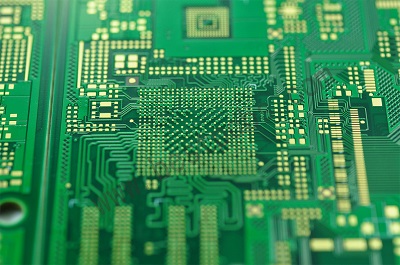
All of us know the printed circuit board, but do you know what is the heavy copper PCB? Best Tech is a very experienced heavy copper PCB fabricator since year 2006. Heavy Copper PCB is a type of printed circuit board that features with thicker copper layers than standard FR4 PCBs. While conventional PCBs typically have copper thicknesses ranging from 1 to 3 ounces (per square foot), heavy copper PCBs have copper thicknesses exceeding 3 ounces and can go up to 20 or more ounces. These copper layers are typically found in the inner and outer layers of the PCB, heavy copper providing enhanced current-carrying capacity and improved heat dissipation capabilities.
The increased copper thickness in heavy copper PCBs allows them to handle higher currents without experiencing excessive heat buildup or voltage drops. This makes them well-suited for applications that require high power handling, such as industrial power supplies, power converters, motor drives, and automotive electronics. Heavy copper PCBs are designed to withstand harsh operating conditions and provide robust performance and reliability.
Today, we would like to talk about the heavy copper PCB used in Industrial Power Supply. In this blog post, we will explore the realm of Industrial Power Supply, delving into the design considerations, material selection, production challenges, exceptional heat dissipation, and unrivaled conductivity of Heavy Copper PCBs. Join us on this enthralling journey as we uncover the secrets behind their application in Industrial Power Supply scenarios, including the testing of inductance, capacitance, and resistance. Get ready to witness the power of Heavy Copper PCBs in the realm of Industrial Power Supply!
Firstly, before you are moving start for the design, it need to get to understand the Design guideline rules of heavy copper PCB.
From the guidelines of heavy copper PCB, it could get to know it encompass considerations such as trace width, trace spacing, and thermal relief patterns. The increased copper thickness necessitates wider traces to accommodate higher currents, while proper spacing is crucial to avoid thermal hotspots and ensure reliable operation. Additionally, selecting suitable materials with excellent mechanical strength and thermal properties is vital to ensure the robustness and longevity of Heavy Copper PCBs. Hope this will bring some ideas to you during your design.
Secondly, as a heavy cooper PCB manufacturing vendor, Best Tech would like to advise the Production Challenges for the heavy copper PCB.
During producing Heavy Copper PCBs presents manufacturers with a set of intricate challenges. Achieving uniform copper thickness across the board’s surface demands advanced plating techniques and precise control over process parameters. Careful attention must be given to the etching process to prevent over-etching, which can compromise the integrity of the copper layers. Moreover, the additional weight of copper requires a sturdy substrate to support the board’s structure. Manufacturers must navigate these challenges with expertise and precision to deliver high-quality Heavy Copper PCBs.
You may have a question in mind, why we need to use the heavy copper PCB for the Industrial Power Supply, because the heavy copper PCB have Exceptional Heat Dissipation and Conductivity: One of the standout features of Heavy Copper PCBs is their unrivaled heat dissipation capabilities. The increased copper thickness acts as a robust conductor, efficiently channeling heat away from power components. This exceptional heat dissipation prevents thermal stress and ensures the longevity and reliability of Industrial Power Supply systems. Additionally, the high conductivity of Heavy Copper PCBs enables efficient power transmission, reducing losses and improving overall system efficiency.
Furthermore, Heavy Copper PCBs undergo rigorous testing to ensure optimal performance in Industrial Power Supply applications. Inductance testing verifies the effectiveness of copper layers in reducing magnetic interference. Capacitance testing evaluates the ability of the PCB to store electrical energy, while resistance testing determines the conductivity and resistance of copper traces. These tests play a crucial role in validating the quality and performance of Heavy Copper PCBs in demanding power supply scenarios.
Heavy Copper PCBs find widespread applications in the field of Industrial Power Supply, particularly in the production of robust and efficient power control products. They are integral components in industrial power converters, motor drives, uninterruptible power supplies (UPS), and various automation systems. The exceptional heat dissipation and high current-carrying capacity of Heavy Copper PCBs make them ideal for handling the power demands of these applications, ensuring reliable and efficient power delivery.
Finally, in the world of Industrial Power Supply, Heavy Copper PCBs emerge as true powerhouses, combining meticulous design, advanced manufacturing processes, and exceptional heat dissipation capabilities. By adhering to design guidelines, overcoming production challenges, and conducting thorough testing, Heavy Copper PCBs prove their mettle in demanding power supply scenarios. As they continue to evolve, these powerhouses will shape the future of Industrial Power Supply, empowering systems with reliability, efficiency, and unrivaled performance. Prepare to witness the electrifying impact of Heavy Copper PCBs in the realm of Industrial Power Supply!
If you have more question heavy copper PCB for Industrial Power Supply, warmly welcomed to contact Best Tech for more get more information of heavy copper PCB which used in Industrial Power Supply. You can visit www.bestpcbs.com to know more about us.
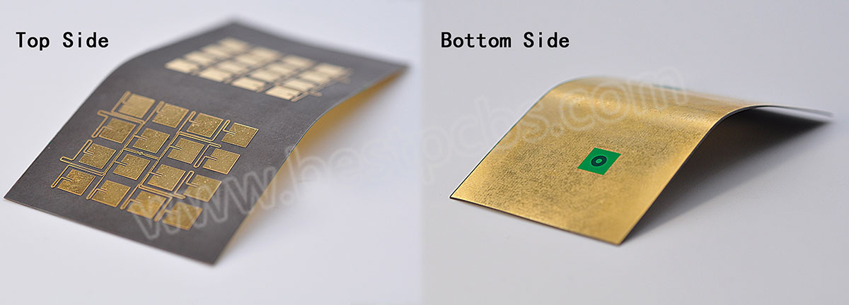
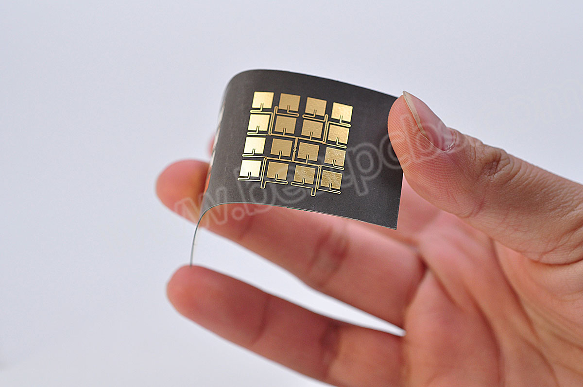
In the ever-evolving realm of printed circuit boards (PCBs), High-Density Interconnect (HDI) technology stands out as a game-changer. HDI PCBs have revolutionized the electronics industry by enabling the creation of smaller, lighter, and more advanced electronic devices. In this blog, let us delve into the captivating world of HDI PCBs, exploring their unique processes and craftsmanship. We also attached some photos for your ref.
What is HDI PCB?
HDI PCBs, short for High-Density Interconnect PCBs, are a specialized type of circuit board designed to accommodate a higher number of components within a smaller footprint. Unlike traditional FR4 PCBs, HDI boards incorporate intricate designs and advanced manufacturing techniques to achieve denser routing and interconnections.
Miniaturization and Component Density
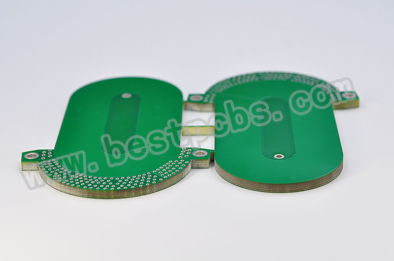
One of the standout features of HDI PCBs is their ability to achieve significant miniaturization. There are fine-pitch traces, microvias, blind and buried vias. You can see the below photo, there are many kinds of the vias.
HDI boards allow for more compact layouts and increased component density. This makes them ideal for applications where space is a premium, such as smartphones, tablets, wearables, and medical devices.
Advanced Manufacturing Techniques
Creating HDI PCBs involves a sophisticated blend of state-of-the-art manufacturing processes. These techniques include laser drilling, sequential lamination, and advanced imaging technologies. Laser drilling enables the creation of microvias, which are tiny holes used for interconnection between different layers of the board. Sequential lamination involves bonding multiple layers together, creating a compact stack-up with enhanced electrical performance. Advanced imaging technologies ensure precise alignment and accuracy during the fabrication process.
Benefits of HDI PCBs
HDI PCBs offer a multitude of advantages that make them highly sought after in today’s electronics industry:
1. Improved Signal Integrity: With their reduced parasitic effects and shorter signal paths, HDI boards provide superior signal integrity and enhanced electrical performance.
2. Increased Reliability: HDI PCBs minimize the risk of failures due to reduced interconnection lengths, better thermal management, and enhanced impedance control.
3. Enhanced Thermal Efficiency: The compact design of HDI boards allows for better heat dissipation and thermal management, ensuring optimal performance of heat-sensitive components.
4. Design Flexibility: HDI technology opens up new design possibilities, enabling engineers to create innovative and compact product designs without compromising on functionality.
Applications of HDI PCBs
The versatility of HDI PCBs makes them indispensable in various industries, including:
Consumer Electronics: Smartphones, tablets, laptops, and wearable devices.
Automotive Electronics: Advanced driver assistance systems (ADAS), infotainment systems, and autonomous driving technology.
Medical Devices: Miniature medical implants, diagnostic equipment, and patient monitoring systems.
Aerospace and Defense: Avionics, satellites, and military-grade electronics.
Industrial Automation: Robotics, control systems, and IoT devices.
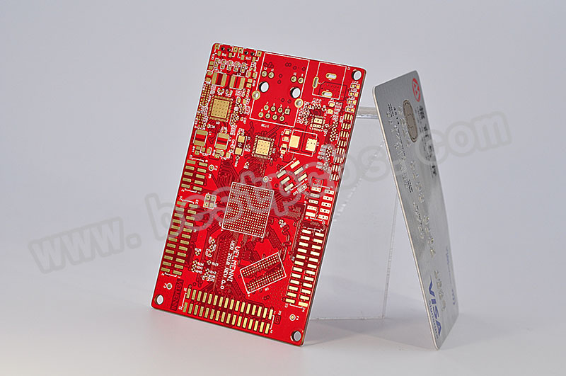
We have many customers from various industries, the PCBs of the below photos are what we produced for our customers.
Conclusion
As technology advances, HDI PCBs will undoubtedly play a crucial role in driving innovation and pushing the boundaries of what is possible in the world of electronics.
We hope this exploration into the captivating world of HDI PCBs can make you know more about HDI PCB. If you’re interested in any HDI PCB, please feel free to contact us any time. Let us supply you an excellent solution and awesome boards for you.
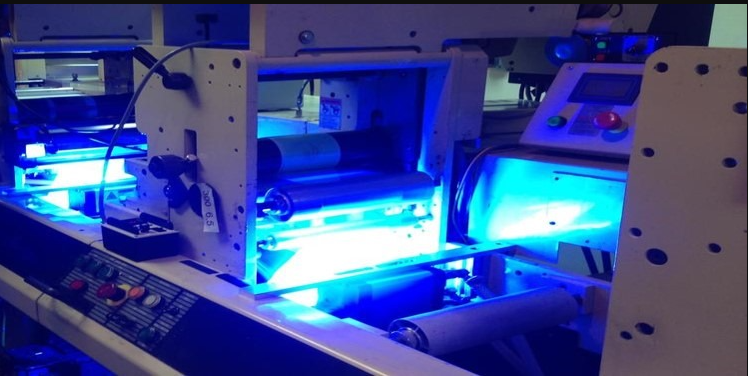
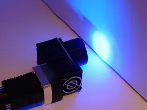
UVLEDs, a subset of light-emitting diodes (LEDs), emit light within the ultraviolet spectrum instead of visible light like traditional LEDs. The UV spectrum is further divided into three main categories based on wavelength: UVA, UVB, and UVC. In this blog, we will explore the critical role of Metal Core Printed Circuit Board (MCPCB) in UVLED technology, highlighting its significance in improving efficiency, heat management, and overall lifespan.
UVA (315-400nm):
UVA, also known as near-ultraviolet, emits long-wave ultraviolet light. It is closest to the visible light spectrum and finds applications in UV curing, forensic analysis, counterfeit detection, tanning beds, and more.
UVB (280-315 nm):
UVB emits medium-wave ultraviolet light and is renowned for its biological effects. It is used in medical treatments, phototherapy, disinfection applications, and even for inducing vitamin D synthesis in the skin.
UVC (100-280 nm):
UVC emits short-wave ultraviolet light and possesses powerful germicidal properties. Its applications include water purification, air disinfection, surface sterilization, and eradication of bacteria, viruses, and other microorganisms.
UVLEDs typically operate within a temperature range of -40°C to 100°C (-40°F to 212°F). However, it is crucial to note that excessive heat can impact the performance, efficiency, and lifespan of UVLEDs. Therefore, appropriate thermal management techniques such as heat sinks, thermal pads, and adequate airflow are commonly employed to dissipate heat and keep UVLEDs within the optimal temperature range.
In conclusion, MCPCB plays a vital role in UVLED technology, offering essential advantages such as efficient heat dissipation, enhanced thermal conductivity, reliability in harsh environments, and electrical isolation. These qualities are paramount for maximizing UVLED performance, ensuring longevity, and maintaining optimal operating temperatures. The significance of MCPCB lies in its ability to enhance efficiency, improve heat management, and provide a reliable foundation for UVLED systems. Without MCPCB, UVLED applications would face challenges in heat dissipation, performance stability, and overall safety.
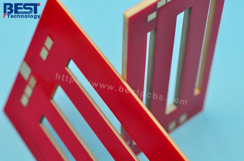
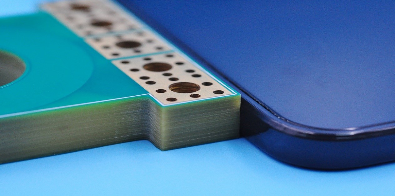
As the demand for higher power and miniaturization of electronics increases, so does the need for Heavy Copper Printed Circuit Boards (PCBs). From our last blog – Why choose Heavy Copper PCB for your High Current Project, we know the heavy copper PCBs are defined as those with copper thicknesses greater than 3 oz. These PCBs are designed to withstand high current and thermal loads, making them suitable for power electronics applications. However, the increased copper thickness also poses challenges during the solder mask printing process.
(16_layers_heavy_copper_PCB_with_10oz_each_layer)
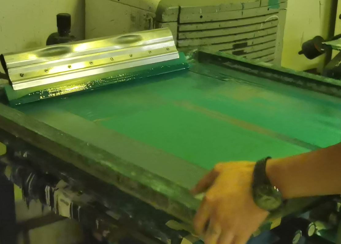
Understanding solder mask
Solder mask (short for S/M in the industry) is a protective coating applied to PCBs to prevent solder bridges and improve solder joint quality. The solder mask is coated to the PCB surface using a screen-printing process, where the desired pattern is created using a stencil and the solder mask ink is then deposited onto the PCB. The ink is then cured, either through heat baking or UV light, to form a solid coating.
There are several types of solder mask materials available, including epoxy, acrylic, and liquid photo imageable (LPI) solder mask. Each type has its advantages and disadvantages, depending on the application requirements.
The benefits of using solder mask in PCB manufacturing include increased reliability, improved solderability, and reduced risk of short circuits and corrosion. The solder mask we usually use is Taiyo, which has high reliability and excellent heat resistance.
(Solder_mask_manually_printing)
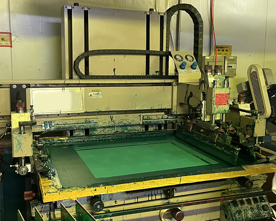
Challenges in solder mask printing of heavy copper PCBs
While solder mask printing is a critical step in PCB manufacturing, the increased copper thickness in heavy copper PCBs presents several challenges for printing process as I mentioned before. It’s difficult to apply enough solder mask to cover thick copper pattern and base material with severe height difference.
1. The high copper thickness and thermal conductivity of heavy copper PCBs make it difficult for the solder mask ink to adhere properly to the surface. This can result in insufficient coverage and registration accuracy, which can affect the overall quality and reliability of the PCB.
2. The high copper thickness can cause stress on the solder mask, leading to mask cracking and peeling. The navigation mark on the substrate has specific ink thickness requirements due to limitations in the ink thickness that can be applied to the substrate. If the ink thickness on the substrate is too thick, it may result in solder resist cracks in the substrate position after the printed circuit board is soldered. This can occur during reflow soldering or thermal cycling, resulting in poor solder joint quality and reduced reliability.
3. The thick solder mask is also more difficult to exposure and develop. If the exposure energy is too weak or not enough, then some undercut problem may happen.
How to overcome this challenge?
To address these challenges, it is essential to choose the right solder mask materials and optimize the application process.
Choosing the right solder mask materials is crucial for ensuring proper adhesion and coverage on heavy copper PCBs. LPI solder mask is often preferred for heavy copper PCBs due to its excellent adhesion and thermal stability. However, epoxy and acrylic solder mask materials can also be used with proper surface preparation.
Optimizing the solder mask application process can also help address the challenges of heavy copper PCBs. This can include using a thinner stencil for improved registration accuracy and applying multiple coats of solder mask for better coverage. Advanced solder mask technology, such as laser direct imaging (LDI), can also help improve registration accuracy and reduce the risk of mask cracking and peeling.
Optimizing the printing process, now in Best Technology, we always make the substrate first, fill the substrate with the solder mask and then treat it as a normal PCB for normal printing solder mask.
(Solder_mask_printing)
If you are in the process of designing a complex multi-layer heavy copper PCB and are looking for a high-quality and experienced manufacturer, feel free to reach out to us at sales@bestpcbs.com, Best Technology can support you by OEM and ODM service to ensure your design is cost-effective and can be easily manufactured.
In the world of electronics, printed circuit boards (PCBs) play a vital role in connecting and powering various components. They are the backbone of every electronic device, from smartphones to industrial machinery. When it comes to designing a PCB for a project, the thickness of the copper layer is an important consideration. Heavy Copper PCB, also known as Thick Copper PCB, has become increasingly popular in charging automotives due to their unique features and benefits. In this article, we will discuss why consider heavy copper PCBs for your high current project.
What a Heavy Copper PCB is?
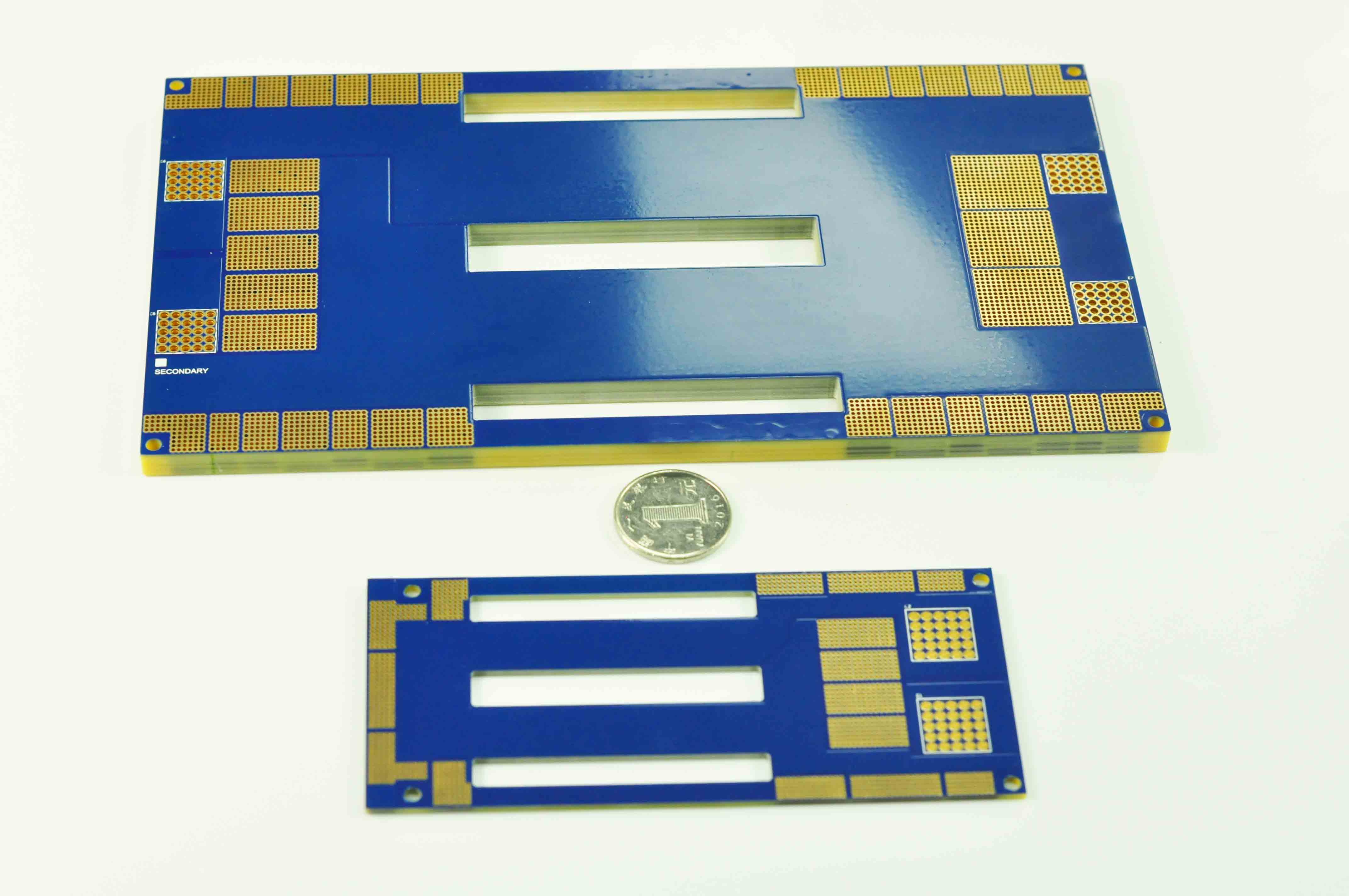
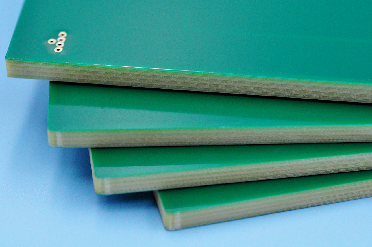
A heavy copper PCB is a circuit board with an unusually thick copper layer, usually exceeding 3 ounces per square foot (oz/ft²). By comparison, standard PCBs typically have a copper layer thickness of 1 oz/ft². Heavy copper PCBs are used in applications where high current is needed, or the board needs to withstand mechanical and thermal stress.
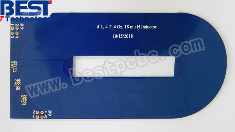
(Heavy_copper_PCB)
Benefits of Heavy Copper PCBs
High Current Capacity
The thicker copper layer in a heavy copper PCB allows for a higher current capacity. This makes it ideal for high-power applications such as power supplies, motor controllers, and industrial equipment. Heavy copper PCBs can carry up to 20 amps or more, compared to the standard 5-10 amps of a regular PCB.
Thermal Management
Heavy copper PCBs are known for their excellent thermal management capabilities. The thicker copper layer allows for better heat dissipation, reducing the risk of overheating and component failure. So that they can generate a lot of heat for the end-application.
Durability
Heavy copper PCBs are more robust and durable than standard PCBs. The thicker copper layer provides better mechanical support, making them resistant to damage from vibration, shock, and bending. This makes them suitable for harsh environments and industrial applications.
Increased Flexibility
Heavy copper PCBs offer increased design flexibility compared to standard PCBs. The thicker copper layer allows for more complex and compact designs, reducing the overall size of the board. This makes them ideal for applications where space is limited, that means you can make a very heavy copper while the size is very small.
Better Signal Integrity
The thicker copper layer in heavy copper PCBs provides better signal integrity. This reduces the risk of signal loss and interference, resulting in more reliable and efficient circuit performance.
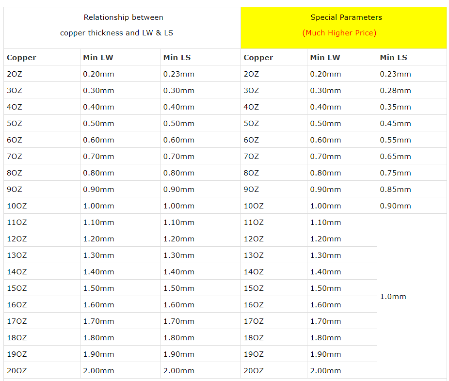
Copper thickness design for a Heavy Copper PCB?
Due to the thickness of copper in heavy copper PCB is thick then normal FR4 PCB, then it is easily to be warped if the copper thickness is not match each other in symmetrical layers. For example, if you are designing an 8 layers heavy copper PCB, then the copper thickness in each layer should follow L8=L1, L7=L2, L6=L3, L5=L4 standard.
Additionally, the relationship between minimum line space and minimum line width also should be considered, follow the design rule will help to smooth production and shorten the lead time. Below are the design rules between them, LS refers to line space and LW refers to line width.
(Heavy_copper_design_rule)
Drill hole rules for heavy copper board
A plated through hole (PTH) in printed circuit board is to connect top and bottom side to make them electricity. And when the PCB design has multi copper layers, the parameters of holes must be considered carefully, especially hole diameters.
In Best Technology, the minimum PTH diameter should be >=0.3mm while the copper ring annular should be 0.15mm at least. For wall copper thickness of PTH, 20um-25um as default, and maximum 2-5OZ (50-100um).
Here are some basic parameters of heavy copper PCB, hope this can help you to understand Best Technology’s capability better.
Base material: FR4
Copper thickness: 4 OZ~30 OZ
Extreme Heavy Copper: 20~200 OZ
Outline: Routing, punching, V-Cut
Solder mask: White/Black/Blue/Green/Red Oil (Solder mask printing is not easy in heavy copper PCB.)
Surface finishing: Immersion Gold, HASL, OSP
Max Panel size: 580*480mm (22.8″*18.9″)
Applications of Heavy Copper PCBs
Heavy copper PCBs are used in a variety of applications, including:
Power supplies
Motor controllers
Industrial machinery
Automotive electronics
Aerospace and defense systems
Solar inverters
LED lighting
(Heavy_copper_PCB_for_high_power_supply)
Choosing the right PCB thickness is crucial for the success of any project. Heavy copper PCBs offer unique features and benefits that make them ideal for high-power and high-temperature applications. If you want to ensure the reliability and performance of your project, consider using heavy copper PCBs. Best Technology has more than 16 years manufacturing experience in heavy copper PCBs, so we are so confident that we can be your most reliable supplier in China. Welcome to contact us at any time for any questions or any queries about PCBs.
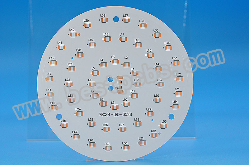
Printed Circuit Boards are the core of the electronics devices, and they exist in everywhere and be everything from your electronic equipment such as mobile phone, computers, so what are they? Let’s explore the secrets together and know why they become more common as technology advances.
What are Printed Circuit Boards?
A printed circuit board also known as PCB for short, is an electronic board for connecting metal circuits by mounting different electronic components in a device and have it do its functions.
PCB is made of fiberglass and laminate materials or a composite epoxy with conductive, it can be made to varies shapes and sizes depends on what applications it will be used for—some have many holes on it while some only have several pads or traces.
In most of devices, we can see there are many components or wires mounted or connected on the surface of PCB, which comes into two different pathways –surface mount and through-hole. Surface mount is a technology that can be abbreviated as SMT, it is a famous technical that mount electronic components (typically SMDs) attached on top of a pad by melted solder paste. Through-hole generally refers to components that have wires through the plated-through-holes that drilled into the circuit board. Both ways are commonly use, but currently with the fast development of the technology advance, surface mount is more popular than through-hole as it is more convenient for production.
What the Functions of Printed Circuit Boards?
The main functions of a PCB is to connect different components and achieve a communication between components and devices, that can be used for everywhere you can think of – Computer, phones, televisions, tablets, cameras, projectors, and so on….
For a simple example, a phone has a PCB that can connect screen, the buttons, cameras, and the circuits on the both sides. Without this board, those components wouldn’t be able to transmit signals and talk to each other and the phone would cease to function.
In addition, electronic equipment using printed board enable to avoid the error of manual wiring, and can realize the automatic insertion or installation of electronic components, automatic soldering, automatic detection by communicate with each other, to ensure the quality of electronic products, improve labor productivity, protect components from damaged, reduce costs, and easy to maintenance.
The advantages of Printed Circuit Boards
PCB performs a number of advantages in electronic industries, a most significant feature is they make products be smaller and more portable as its density circuits and components communication. The density circuits on PCB allows it take up much space for components so you can get a smaller product.
High density
Over the past decades, the high density of printed boards has been developed with the improvement of integrated circuits and the advancement of installation technology.
High reliability
Through a series of checks, tests and aging tests, the PCB can be guaranteed to work reliably for a long time (generally 20 years).
Designability
For various performance (electrical, physical, chemical, mechanical, etc.) requirements, can PCB be achieved to such requirements in short time and high efficiency according to design standard rules.
Maintainability
By means of standard PCB design rules, once the program or device failure, users fix the devices quickly.
Cooling abilities
Overheating is one of the biggest reasons of electronics failure, so by keeping them cool with a PCB, you can increase the lifetime of your product.
Types of Printed Circuit Boards
Best Technology provides different kinds of PCBs and PCBAs for our customers, for a quickly reviewing, we listing as below:
Rigid Printed Circuit Board (FR4-PCB)
Flex Printed Circuit Board (FPCB)
Rigid-Flex PCB
Metal Core Printed Circuit Board (MCPCB)
Ceramic Board
SinkPAD Board
Other special PCB such as heavy copper PCB, HDI PCB, RF PCB, and so forth
PCB assembly
In a word, with the development of electronics, it’s necessary to have a functional part like the PCB that can keep up with the demand. Next step, contact us if you have PCB demands.
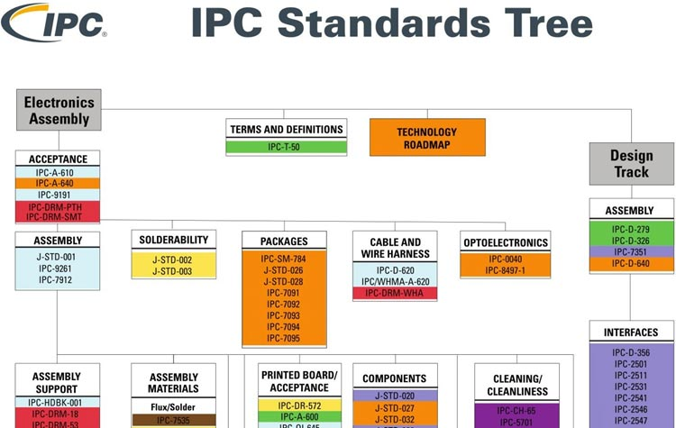
Do you know what is IPC standard for PCB?IPC, it is a trade association whose goal is to standardize the assembly and production requirements of electronic devices and components. It was established in 1957 as the Institute of Printed Circuits. IPC has developed thousands of standards and specifications to regulate the electronics manufacturing industry.
IPC standards are related to PCB design, production technology, electronic assembly, etc., in order to achieve high reliability, high quality, high performance, and meet user specifications.
What are the IPC Standards for?
Before we can understand IPC standards, we first need to know who made them. It comes from the IPC Association, a trade association whose goal is to standardize assembly and production requirements for electronic devices and components. It was founded in 1957 as the Printed Circuit Research Institute. Its name was later changed to the Institute for Electronic Circuit Interconnection and Packaging to highlight the expansion from bare boards to packages and electronic components. In 1999, the organization officially changed its name to IPC with the slogan “Association Connecting Electronics Industries”.
IPC standards are the most widely recognized code of acceptability in the electronics industry. The organization publishes standards for nearly every stage of the electronic product development cycle, including design, procurement, assembly, packaging, and more. In other words, IPC standards refer to everything in the electronics industry and are the basic knowledge of designers and manufacturers.
Just like the IPC standards tree, there are many different aspects of standards that all serve the end product. IPC-A-610, for example, focuses on the acceptability of electronic components and is used worldwide by original equipment manufacturers and EMS companies.
What is the PCB IPC Standard?
IPC plays a vital role in the PCB industry by establishing standards that cover every stage of PCB production from design to manufacturing. These standards ensure consistency and compatibility throughout the PCB process. During the design phase, IPC standards guide file formats, PCB design software, design guidelines, and electronic product documentation. They also affect the material selection of PCB components, surface mount equipment and surface treatments. In addition, these standards are essential for testing and evaluating the acceptability of printed boards.
When it comes to welding, IPC standards cover a variety of techniques, including reflow soldering, wave soldering and welding. These guidelines help companies determine whether their electrical and electronic components meet quality expectations during manufacturing. IPC standards also address cable and harness assemblies to ensure they meet standards.
The most widely recognized IPC standard for PCBs is IPC-6011, which Outlines the performance requirements for PCBS. However, IPC-6012 is more specific and governs the qualification and performance of rigid PCBs. IPC-6012 covers everything from how the PCB should be made to its thickness and the integrity of the copper layer. Compliance with this standard ensures that PCBs meet electrical and mechanical performance expectations. Whether you’re creating boards for high-end computers or small consumer devices, compliance with PCB IPC standards is critical to meeting industry and customer expectations. Here is the IPC tree for your reference:
What is the IPC Level of PCB?
One of the most widely used industry standards in the manufacturing of printed circuit boards is IPC-A-610C Acceptability of Electronic Assemblies and IPC-A-600 Acceptability of Printed Boards. This standard is used primarily for the incoming inspection of bare boards from a PCB fabricator.
In the IPC-A-610C document, electronic products are divided into level 1, level 2, and level 3. The higher the level, the stricter the quality inspection conditions. Here are how 3 levels divided:
Level 1 products: called general-purpose electronic products. Including consumer electronic products, certain computers and their peripherals, and products whose main purpose is to use functions.
Level 2 products: called dedicated service electronic products. Including communication equipment, complex industrial and commercial equipment and high-performance, long-life measuring instruments. Under normal use environment, this kind of product should not malfunction.
Level 3 products: called high-performance electronic products. Including high-reliability, long-life military and civilian equipment that can continue to operate. This kind of product must not allow any interruption failure during use, and at the same time, it is necessary to ensure the reliable startup and operation of the equipment in a harsh environment. Such as medical life-saving equipment and all military equipment systems.
For PCB manufacturing, do you know which IPC standards are commonly used?
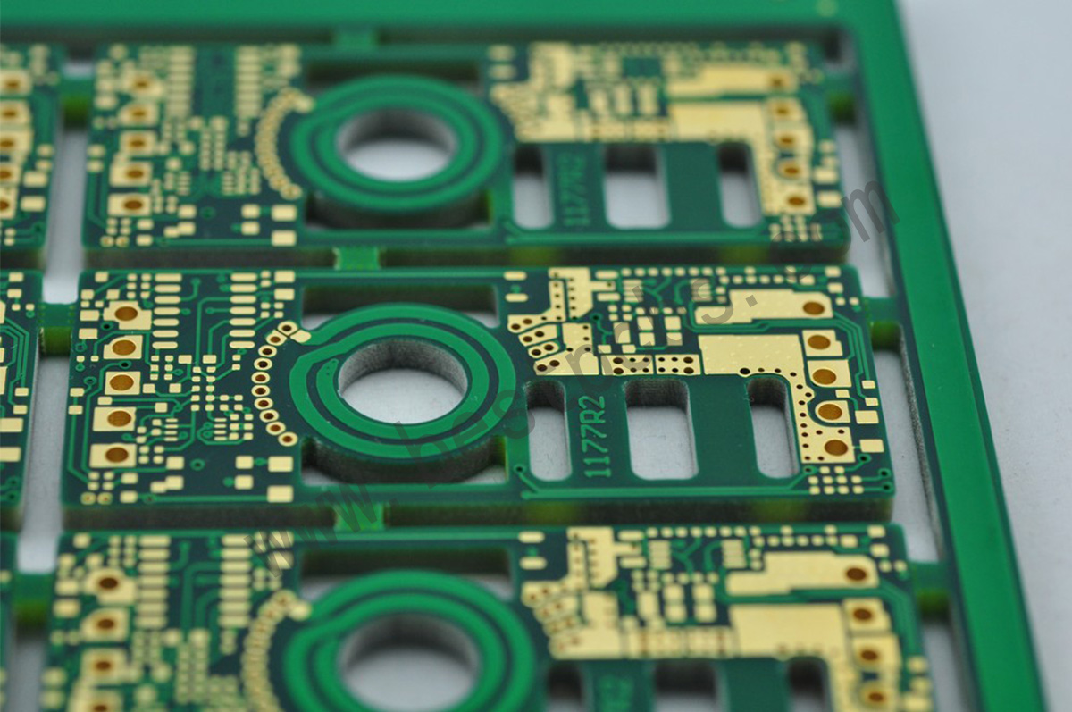
multilayer pcb
IPC Standard for PCBs
The IPC has created several standards for printed circuit board (PCB) design, manufacturing, and assembly. Here I would like to share you some standards which we mainly use:
IPC-2221
A general standard that covers almost every aspect of PCB design, including electrical considerations, thermal design, and manufacturing-ready design.
IPC-2222
A guide for rigid PCB cross-sectional design, including recommendations for board thickness, hole aspect ratio, and dielectric clearance.
IPC-2223
A standard for reliable Flex-PCB design, including guidelines for material selection, impedance control, and pad placement.
IPC-2224
A standard for PC card form PCBs, including design requirements for organic and inorganic materials, and single, double, or multilayered interconnections.
IPC-A-610
A standard for PCB assembly that classifies PCBs into three quality levels, with Class 1 being the lowest and Class 3 being the highest.
IPC-6011
General Performance Specification for Printed Boards
IPC-6012
Appraisal performance and specifications for Rigid printed boards
IPC-6013
Appraisal performance and specifications for Flexible printed boards
Appraisal and performance of permanent performance
IPC-HM-860
Multilayer Hybrid Circuit Specification
J-STD-003
Solderable test for printed boards
IPC-A-600F
Acceptance conditions for printed boards
IPC-4761
Design Guide for Protection of Printed Board Via Structure
resin filled production bpm20599
What is IPC-A-610 Standard?
IPC-A-610 Standard is one of the most widely recognized standards in the electronics industry, specifically focusing on the acceptability of electronic assemblies. It provides detailed guidelines and criteria for the inspection of PCB assemblies, so that these assemblies meet the necessary quality levels for their intended use. Its main content includes:
1. Soldering Criteria
IPC-A-610 provides in-depth guidelines on acceptable soldering techniques, covering solder joints, surface mount devices (SMDs), through-hole components, and wire terminations. It explains what constitutes an acceptable versus defective solder joint, ensuring that the electrical connections are reliable.
2. Component Placement
The standard includes criteria for the correct placement and alignment of electronic components on PCBs. It specifies the acceptable tolerances for misalignment and ensures components are correctly placed for proper electrical performance and physical integrity.
3. PCB Assembly Defects
IPC-A-610 details different types of assembly defects, such as insufficient solder, tombstoning, lifted pads, and more. Each defect is categorized based on its severity and impact on the function and reliability of the product, providing guidance on whether a defect can be accepted or if it requires rework.
4. Classes of Electronic Assemblies
The standard divides electronic assemblies into three classes based on the end-use of the product:
Class 1 – General electronic products
Class 2 – Dedicated service electronic products
Class 3 – High-performance products
5. Mechanical Assembly
IPC-A-610 provides criteria for the mechanical aspects of PCB assemblies, such as mounting hardware, screws, connectors, and wire routing.
6. Coating and Potting
The standard covers the application of protective coatings (conformal coatings) and potting materials that protect the PCB from environmental damage such as moisture, dust, or chemicals. It specifies acceptable thicknesses, coverage areas, and inspection methods.
7. Cleaning Requirements
The cleanliness of PCB assemblies is critical for preventing performance degradation over time. IPC-A-610 outlines acceptable levels of residues from fluxes and other contaminants and specifies methods for inspecting and verifying cleanliness.
8. Cable and Wire Harness Assemblies
The standard includes requirements for assembling and inspecting cable and wire harnesses.
9. Solderless Wire Wraps
The standard also touches on solderless wire-wrapped connections, which are used in some applications where soldering is not practical or preferred. IPC-A-610 defines the acceptable criteria for such connections.
10. Inspection and Testing
The IPC-A-610 standard provides guidelines for visual inspection and testing methods used to evaluate whether an assembly meets the required acceptability criteria. This can include both automated and manual inspection processes, depending on the class of product.
Why IPC Standard is Important?
IPC standards are of great importance to the circuit board industry.
1. IPC standard specifies the requirements for all aspects of the design, manufacturing and assembly of the circuit board, including material selection, size specifications, welding quality, reliability testing, etc., providing a unified reference and guide for circuit board manufacturers to improve product quality and reliability.
2. IPC standards can help communicate and cooperate between PCB manufacturers and customers. By referring to IPC standards, the two parties can reach a consensus on PCB specifications, quality requirements and other aspects, reduce misunderstandings and disputes, and improve production efficiency.
3. For customers, IPC standards provide confidence. When a company adheres to these standards, they can trust that the final product will be reliable and durable, even in demanding environments.
4. In addition, IPC standards also contribute to the technological innovation and development of the circuit board manufacturing industry. By being in line with international standards and understanding the latest technological trends and standard requirements, manufacturers can continuously improve production processes and equipment, improve production efficiency and product quality, and enhance competitiveness.
At the same time, IPC regularly updates and revises standards to meet changing technology and market needs.
What is the IPC Standard for PCB Clearance?
PCB clearance, or the distance between conductive components, is essential to avoid electrical shorts or interference. Without proper clearance, electrical shorts could occur, potentially leading to device failure or safety hazards. The IPC-2221 standard covers PCB design and provides guidelines for this clearance, ensuring safety and functionality. This standard specifies how much space is needed between traces, pads, and other conductive materials depending on the operating voltage. However, the minimum clearance between any two conductors on a PCB depends on the device’s intended use and voltage:
General-purpose devices: 0.1 mm (4 mils)
Power conversion devices: 0.13 mm (5.1 mils)
Class 2 and 3 PCBs: 0.25 mm (10 mils) for low voltage and 0.5 mm (20 mils) for high voltage
What are the IPC Standards for PCB Repair?
PCB repair can be tricky, but IPC-7711/7721 offers guidance on how to properly rework and repair PCBs. These standards provide detailed procedures for everything from removing defective components to repairing damaged traces and soldering issues.
By following IPC-7711/7721, technicians can restore a PCB to its original condition without compromising its performance. This is critical in industries where PCBs are expensive or difficult to replace, such as aerospace and medical devices. Repair standards also reduce the environmental impact by extending the life of the PCB, making repairs more sustainable.
It is no problem for us to manufacture the PCB following the standard in IPC 6012 /6013 Class 2 and Class 3, as well as following to the standard listed above. These acceptance conditions are the basis for the inspection of our company’s products, as well as the working standards of the employees at the production site, and also become an important part of the training of the employees for PCB production and assembly in our company.
Send us your PCB drawing, let’s help to make your PCB design into a real board.
In Best Technology, solder mask and silkscreen are available in a variety of colors. For example, common colors of solder mask are black, white, blue, green, red. Common silkscreen colors are black, white, yellow, red, blue. Generally according to the different needs of customers to use collocation, but sometimes if the color collocation is not appropriate will produce color difference.
The following is a list of common collocations that we recommend based on our experience for your future project design.
functionality.But if the color of the silk screen does not match properly,which may
Cause chromatic aberration(for example,a yellow silkscreen on a black solder mask,
The silkscreen visual may look green)or make reading the silk screen more difficult
To read(for example, a black silkscreen on a light black solder mask).The solder mask will also affect your ability to visually inspect the PCBs. Below are the solder mask comparison from the highest contrast to the lowest for your reference.
Green
Most customers will choose to use Green solder mask for their project since Green is easy on the eyes and allows for high contrast between traces, planes, and empty space on the PCB. Green solder mask has become an industry standard. High contrast allows technicians to most easily review for manufacturing defects.
green
Red
A Red solder mask will provide a bold and clean looking PCB, however the contrast between traces, planes, and empty space significantly lower than it is with a green solder mask. Magnification may be needed when inspecting fine traces on the board for defects with a Red mask. White silkscreen will be better than black silkscreen on a board with red solder mask.
red
 Blue
Blue solder masks have even lower contrast, and magnification becomes required when inspecting for manufacturing defects. These PCBs look visually pleasing and professional and are a good choice for fully-developed products that will not require trace visibility.
blue
Black
Black masks have almost no contrast between traces, planes and empty space. A Black mask will absorb heat, increasing the danger of overheating for sensitive components. Pay attention that in order to avoid the appearance of color difference as far as possible do not choose the silkscreen like yellow, green, red, or blue. White will be the better choice.
black
White
A white mask will be the hardest to clean, and also has the lowest contrast. If possible, we suggest that you avoid choosing white, especially in the prototyping stage. It’s the best choice to use white solder mask for LED board, following pictures for your reference.
whtite
If you have other questions about solder mask, welcome to contact us. (Email:sales@bestpcbs.com), we will prove you professional suggestions and solutions.
For PCB materials, you may have ever heard about many different kinds of materials such as the materials of FR4, Aluminum, Copper base and ceramic base.
But do you know what the duriod 5880 materials is?
Actually duriod 5880 is a kind of materials of the Rogers, it is the materials which is used for high frequency circuit board. RT 5880, which is famous for its low dielectric loss, low moisture absorption, and stable dielectric constant. The PCB made of duriod 5880 can be widely used in airborne and ground-based radar systems, millimeter wave applications, and space satellite transceivers. Different with other kinds materials, the color of the RT 5880 materials is black.
Why this material can be used in such high end field? Let’s see below to know more information.
Excellent dielectric properties: RT/duroid 5870/5880, as a new generation of high-frequency laminate, is made of polytetrafluoroethylene composite material (PTFE). At the same time, glass microfibers are randomly distributed in the material, which provides the greatest strength during the production and application of the circuit board.
High-frequency circuit design has strict requirements on the dielectric constant of the printed circuit board. RT/duroid 5880 has an ultra-low dielectric constant and remains the same in a very wide operating frequency range.
At 10GHz operating frequency, the measured dielectric constant is only 2.33/2.2, which is significantly lower than similar materials on the market. Therefore, from the perspective of performance parameters and production costs, the board is more suitable for high-frequency application design than similar products.
At the same time, under the same standard (f=10GHz), and the dielectric loss of the RT5880 is only 0.0012/0.0009. The extremely low dielectric loss makes it very suitable for high-frequency and the field of wide-band applications which requiring minimal dispersion and low loss.
In addition, the extremely low moisture absorption rate makes it an ideal choice for applications in high humidity environments. The moisture absorption rate of RT/duroid 5880 is only 0.02%, so it can meet the strict requirements of mechanical reliability and electrical stability in the complex microwave structure design, and it is also suitable for applications in high humidity environments.
With the continuous improvement of the operating frequency of high-frequency circuits, the requirements for the dielectric constant and dielectric loss of the circuit board are becoming more and more stringent. The excellent performance of RT/duroid 5880 in these two aspects can significantly improve the design of high-frequency circuits. Definity, improve circuit performance.
Easy to process and install In this high-frequency design, in order to meet the requirements of electromagnetic shielding and compact design, printed circuit boards are often installed in various irregularly shaped cavity structures. Therefore, the PCB board must be designed in different shapes and suitable for production and Installation.
For RT/duroid 5880 laminate, which is easy to cut, trim and good for PCB manufacturing.
At the same time, it can resist all the solutions and chemical agents used in the process of etching and plating through holes, and it has a good performance of the cold and heat resistance.
The composite material RT/duroid 5880 can be covered with a laminated copper foil for some key electrical applications, and brass plates or copper can also be used as required. Usually laminates of the RT/Duriod 5880, it can make double-sided copper clad with thicknesses ranging from 1/2 oz. to 2 oz./ft2 (8.5~70 μm) to meet most custome’s requirements for the thickness of copper foil.
Our company has focus on the PCB fabricationi for more than 15 years, we can make PCB with Rogers PCB with RT/Duriod 5880, as well as RO4003C and RO4350B with different thickness. If you are interesting to know more and your PCB also want to made of RT/Duriod 5880, please feel freely to contact us for more information related.