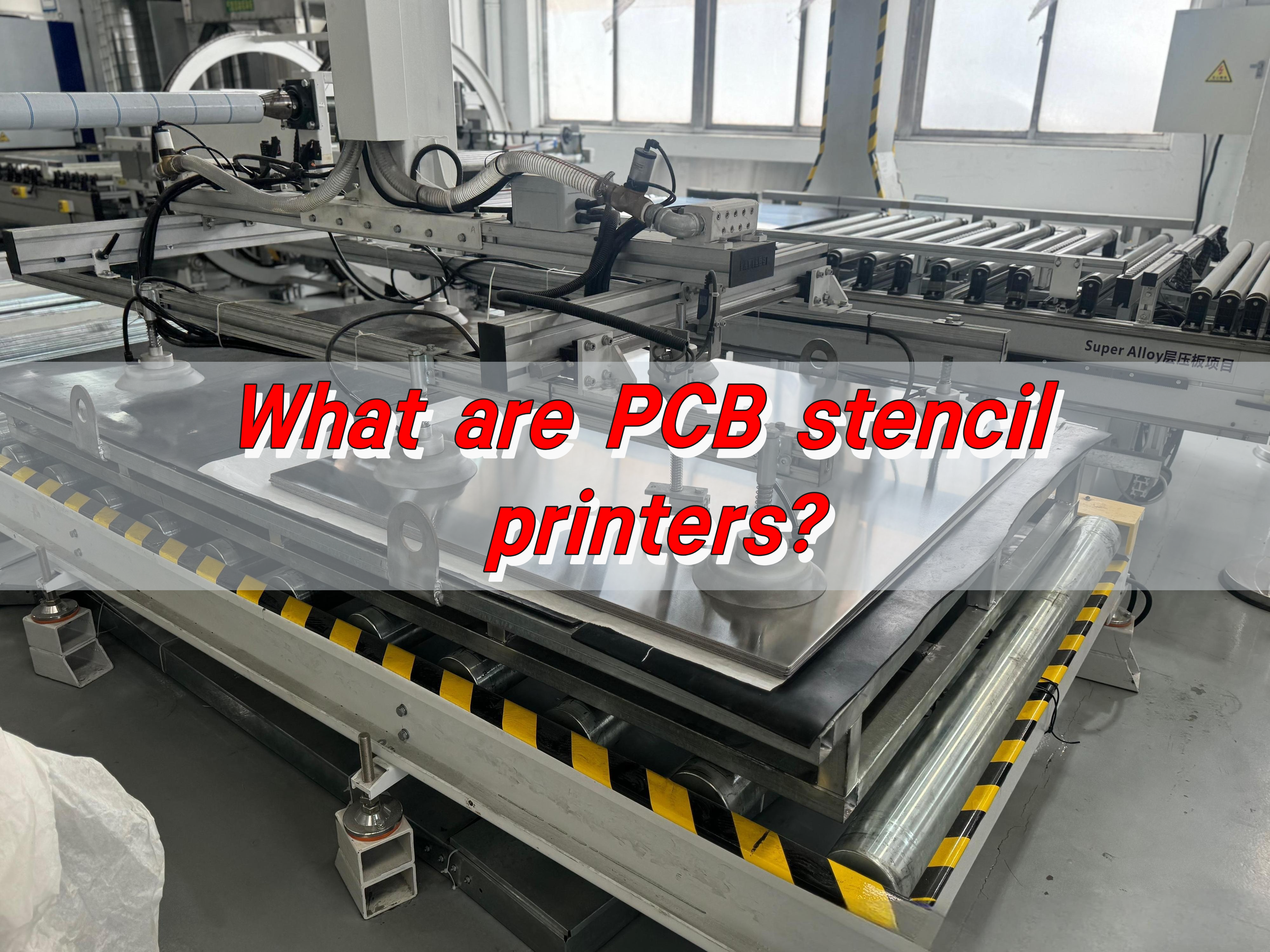
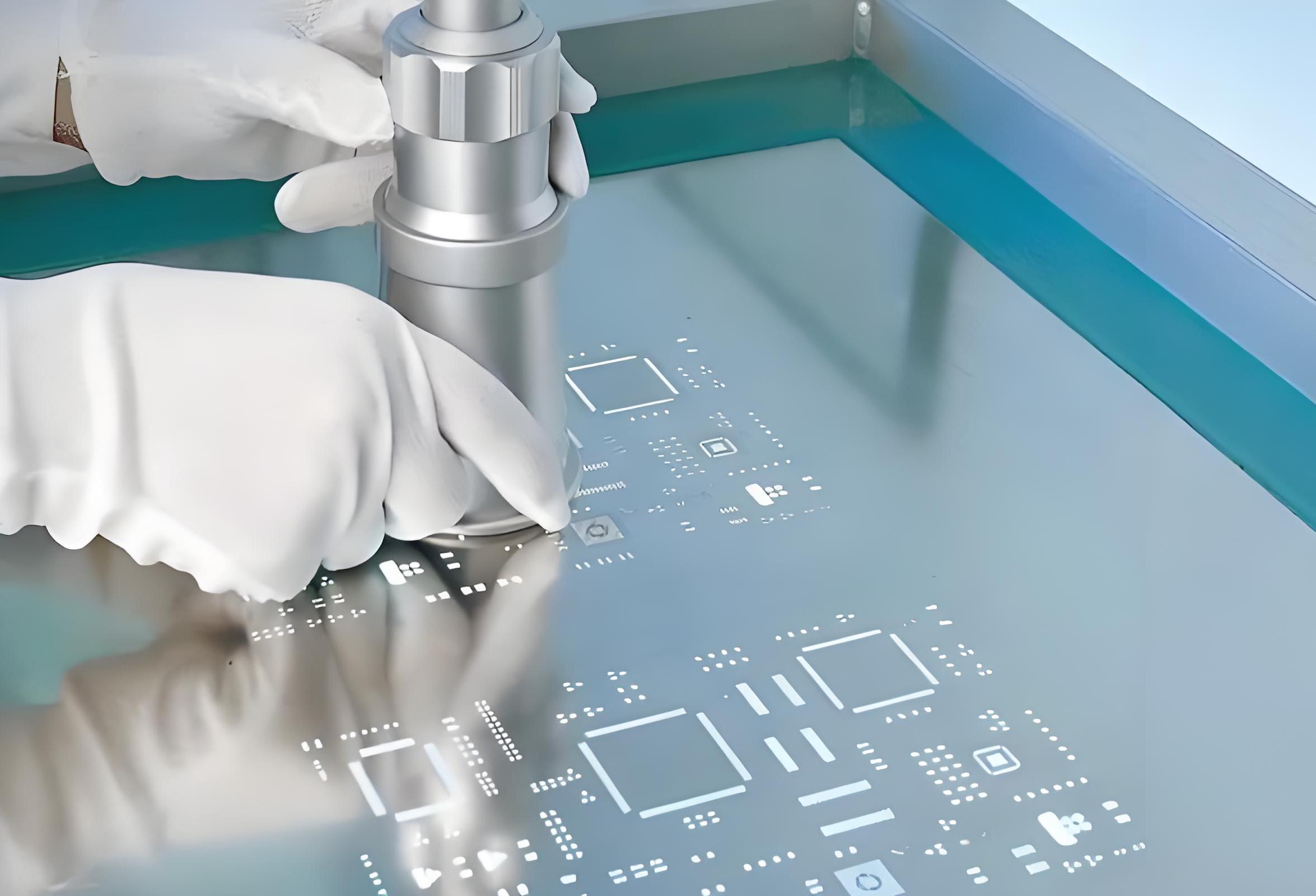
What are PCB stencil printers? stencil pcb printers is a process for applying solder paste to specific pad locations on a PCB board with high precision. The core tool is the PCB stencil, a thin sheet of precision-machined metal with holes that exactly match the shape, size, and location of the PCB board pads.
What is a PCB stencil?
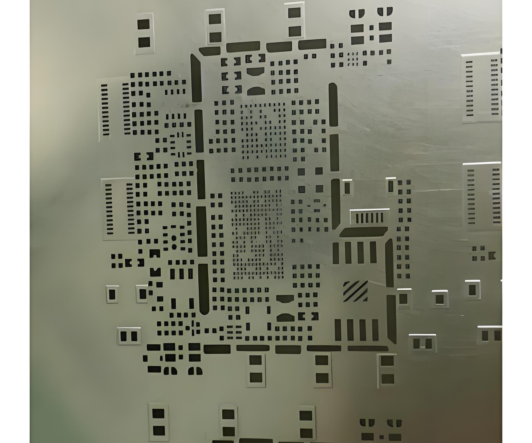
A stencil in PCB refers to a tool used in the surface mount assembly process to precisely deposit solder paste at specific locations on a printed circuit board. The stencil is usually made of brass or stainless steel and is engraved with circuit patterns that match the locations of surface mount devices (SMDs) on the PCB.
The stencil plays a vital role in the PCB assembly process. It ensures that solder paste is accurately deposited at the locations of the SMDs, thereby ensuring that the components are accurately mounted in the correct locations.
The design of the stencil, including its composition, thickness, and the shape and size of the holes, will affect the quality of the solder paste deposition. Too much or too little solder paste can lead to welding quality problems, such as ball formation, bridging or tombstoning.
What is a PCB stencil made of?
PCB stencils are mainly made of stainless steel, which has good corrosion resistance and high hardness. This stencil is usually called a SMT Stencil or a solder paste printing stencil, which is mainly used to print solder paste onto PCB circuit boards during SMT assembly.
The stencil is cut by high-precision laser, and has holes or grooves corresponding to the PCB pads, which are used to accurately control the printing of solder paste.
What types of PCB stencils are there?
The types of stencil in PCB stencils mainly include the following:
- AI stencil: mainly used in SMT process, can replace dispensing machines, improve production efficiency and reduce costs.
- Laser stencil: through high-energy laser cutting to create an opening that perfectly matches the PCB pad, it has the advantages of high precision and smooth edges, and is particularly suitable for high-density and high-demand PCB assembly.
- Etched stencil: The opening is formed by chemical etching liquid corroding the steel sheet. The cost is lower, but the accuracy and edge smoothness are not as good as laser cutting.
These stencil types have their own characteristics and are suitable for different PCB manufacturing needs. Laser stencils are particularly suitable for high-density and high-demand PCB assembly due to their high precision and smooth edges; while etched stencils are suitable for applications with low precision requirements due to their low cost and simple manufacturing process.
What is the function of a PCB stencil?
The stencil in the PCB template plays a vital role in the manufacturing process. The stencil is a high-strength metal grid that is mainly used to apply solder paste on the PCB. Its specific functions include:
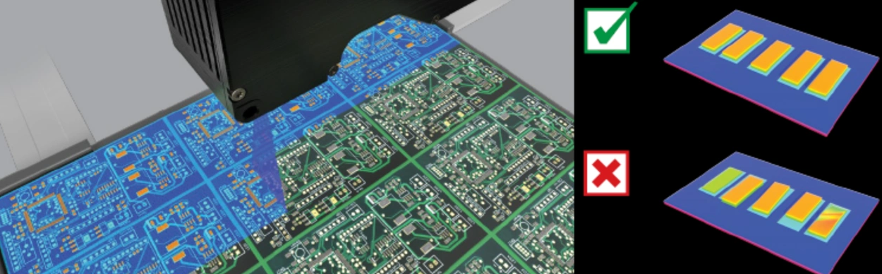
- Accurate quantitative distribution of solder paste: The stencil accurately controls the distribution of solder paste through the holes on it, ensuring that the solder paste is evenly and accurately applied to the predetermined pad position on the PCB, avoiding too much or too little solder paste, thereby ensuring welding quality.
- Improve welding quality: By precisely controlling the distribution of solder paste, stencil helps reduce welding defects such as bridging and empty soldering, improves the consistency and reliability of welding, and thus improves the electrical performance of the entire PCB and the overall quality of the product.
- Adapt to complex designs: With the trend of miniaturization and high density of electronic products, the components on PCBs are getting smaller and smaller, and the spacing is getting closer and closer. Stencil can be customized according to design requirements to meet the needs of high-end electronic products.
- Improve production efficiency: On an automated production line, with the use of precision stencil and automatic solder paste printers, fast and efficient mass production can be achieved, greatly improving production efficiency and reducing the error rate of manual operation.
How to design a PCB stencil?
In the surface mount (SMT) assembly process, solder paste stencil plays a key role. Its ability to accurately apply solder paste is directly related to the quality and reliability of the connection between SMD components and PCB pads. The following are the key points to focus on when designing solder paste stencils:
- Matching design files: The design of solder paste stencils must be closely constructed based on the solder paste layer information of the PCB to ensure that every hole and shape on the stencil is precisely matched with the solder paste layer, so as to provide an accurate basis for subsequent solder paste coating and avoid poor welding problems caused by design deviations.
- Selection and thickness: There are many types of solder paste stencils, the most common of which are stainless steel stencils and polymer stencils. At the same time, the determination of stencil thickness cannot be ignored. It is usually in the range of tens to hundreds of microns. It needs to be finely adjusted in combination with factors such as pad size, pin spacing, and required solder paste amount to ensure uniformity and stability of solder paste coating.
- Hole size and shape: The hole size and shape of the stencil should be perfectly matched with the solder paste area on the solder paste layer, and the solder paste coating range should be strictly controlled to prevent the solder paste from overflowing to the adjacent pads and causing short circuit failures, or insufficient solder paste coating affecting the welding quality, to ensure that the solder paste coating is accurate at every location.
- Customized special design: For special components or parts with special pin structures, a special design scheme is required on the solder paste stencil.
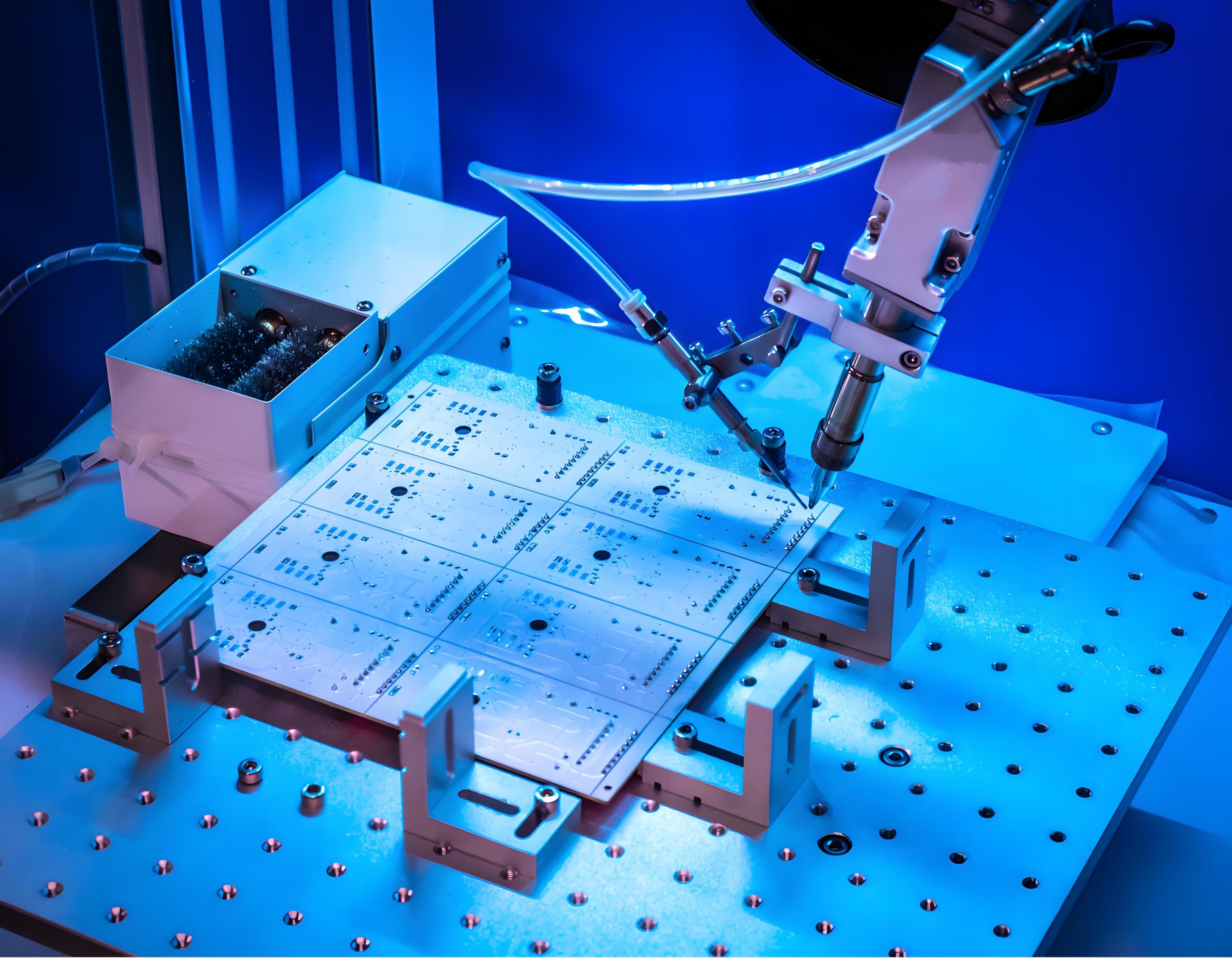
How to use a PCB stencil?
The following are the steps to use a PCB stencil:
1. Preparation:
- Check whether the PCB stencil opening is blocked or deformed, and whether the PCB board surface is clean.
- According to the size of the printer and the stencil, install the stencil through the positioning hole and the printer positioning pin to ensure the correct direction and secure fixation.
2. Solder paste preparation:
- Select solder paste according to PCB welding requirements and component type, check the shelf life and quality, take it out and stir it for 3-5 minutes to make it uniform.
3. Solder paste printing:
- According to the thickness of the stencil, opening and solder paste characteristics, adjust the parameters such as the printer scraper pressure, printing speed), demolding speed and stroke.
- Start the printer, and the scraper moves to fill the stencil opening with solder paste and transfer it to the PCB pad. Observe the printing situation during the process and adjust it in time if there is any problem.
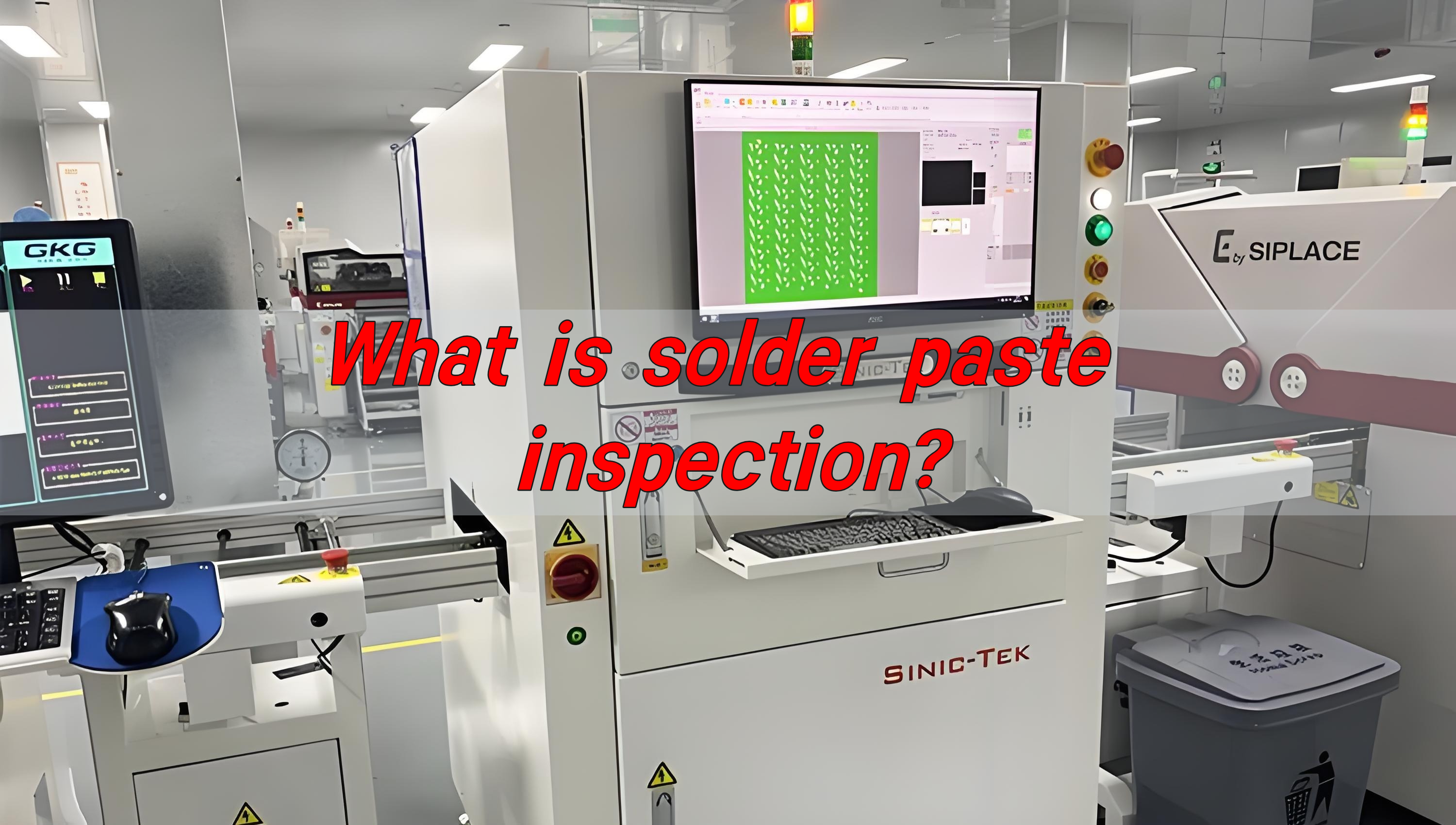
4. Post-printing inspection and cleaning:
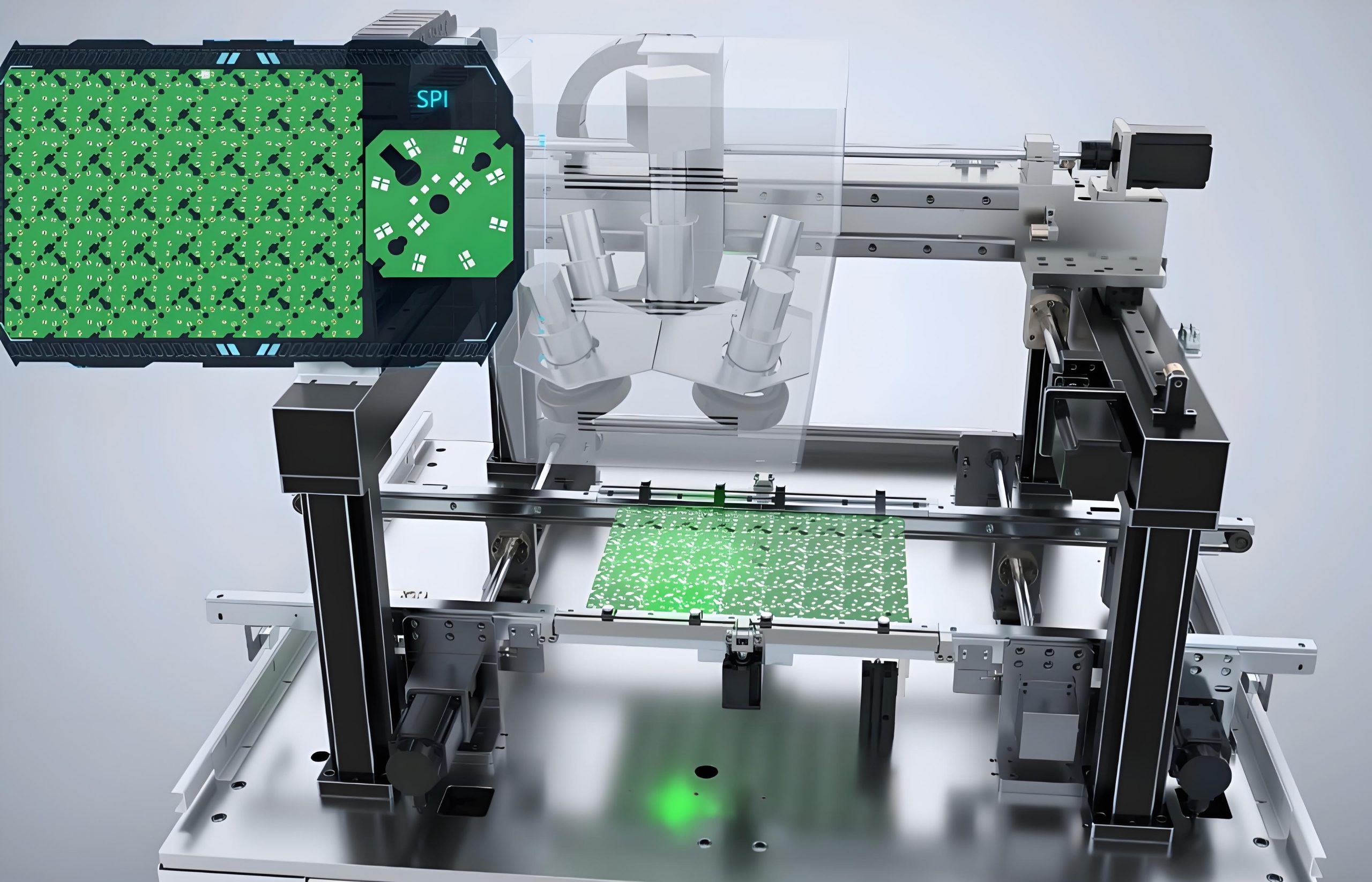
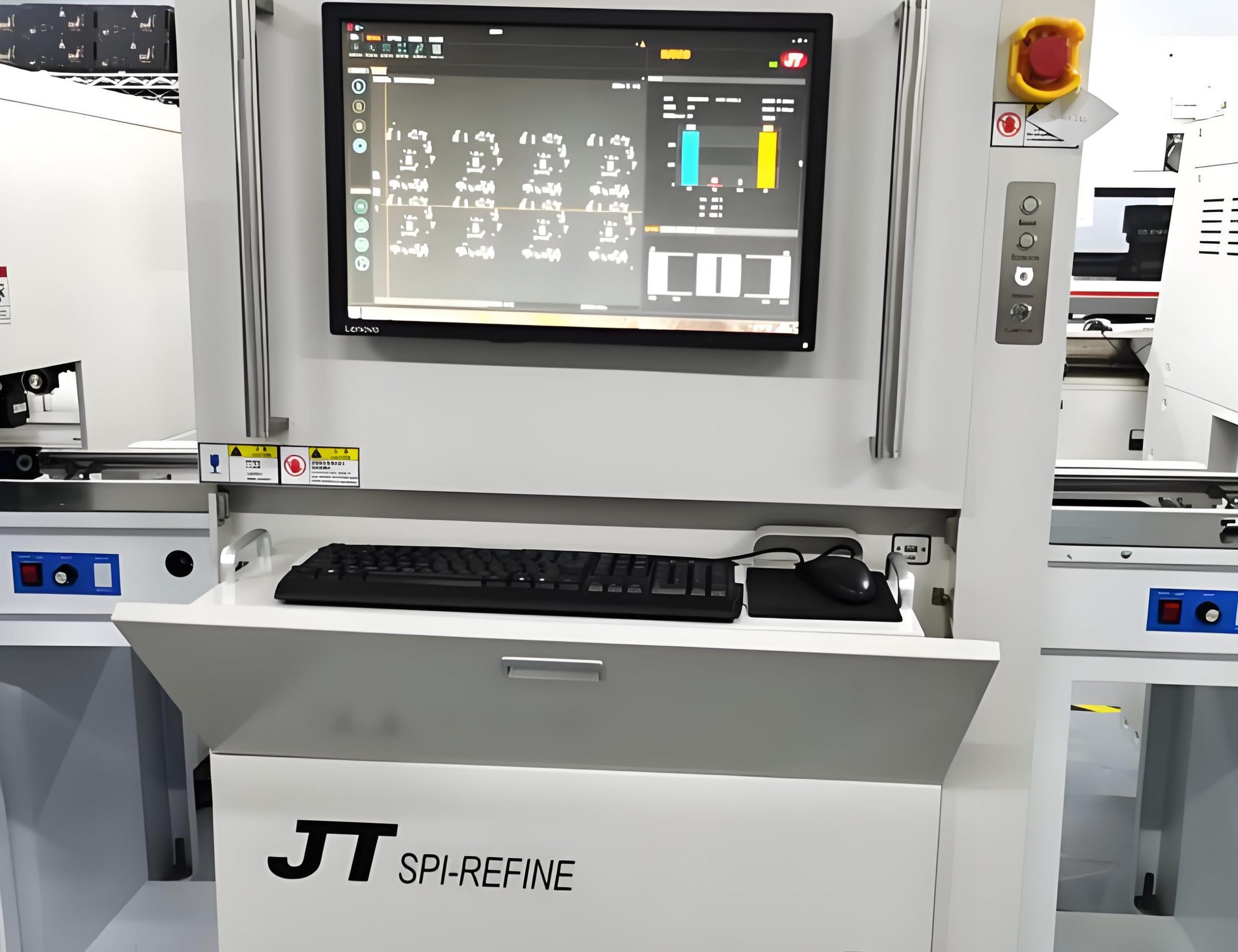
- Use a magnifying glass or SPI to check the quality of solder paste printing on the PCB board, and reprint the unqualified ones after cleaning.
- Use special solvents and tools to clean the template, remove the residual solder paste, and store it properly after drying.
PCB stencil printing is an indispensable key process in the field of electronic manufacturing. As a core tool, the quality and precision of the stencil directly determine the coating effect of the solder paste on the PCB board, which in turn affects the welding quality of electronic components, and ultimately plays a decisive role in the performance, reliability and stability of electronic products.