SMD LED PCB board design is very important in electronic products industry. From precise pad layout to efficient heat dissipation solutions, every detail is related to light efficiency and life. Whether it is rapid iteration in the prototype verification stage or cost optimization in the mass production stage, professional design needs to integrate electrical performance and process compatibility. In this blog, let’s learn together how to design SMD LED PCB boards and how to choose a good SMD LED PCB manufacturer.
If you want to move design to prototype and manufacture, Best technology can meet your all requirements for SMD LED PCB Board. Because we specializing in SMD LED PCB Board design, prototyping and production over 18 years, and we have an experienced PCB designers team who can give you free technical support. And we can provide you PI Analysis, SI Analysis, EMC Testing with the SMD LED PCB you designed. Then we can provide you with customized services (including customized Logo) with low MOQ (one piece is okay) at reasonable prices. You can feel free to contact us sales@bestpcbs.com if you have any request for SMD LED PCB.
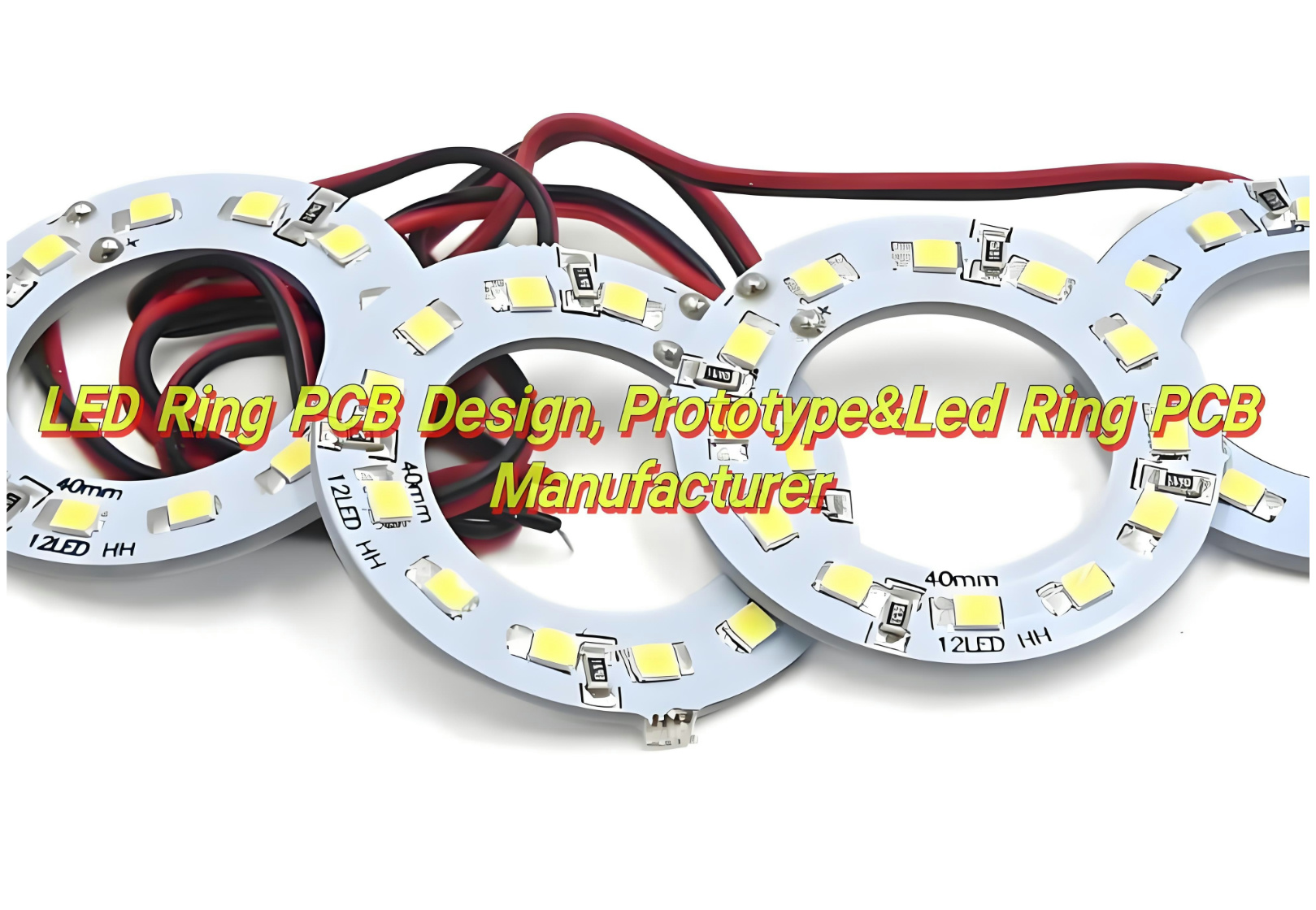
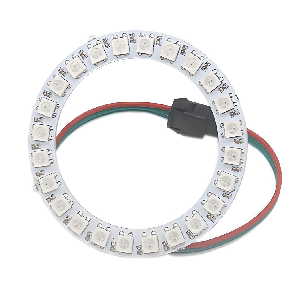
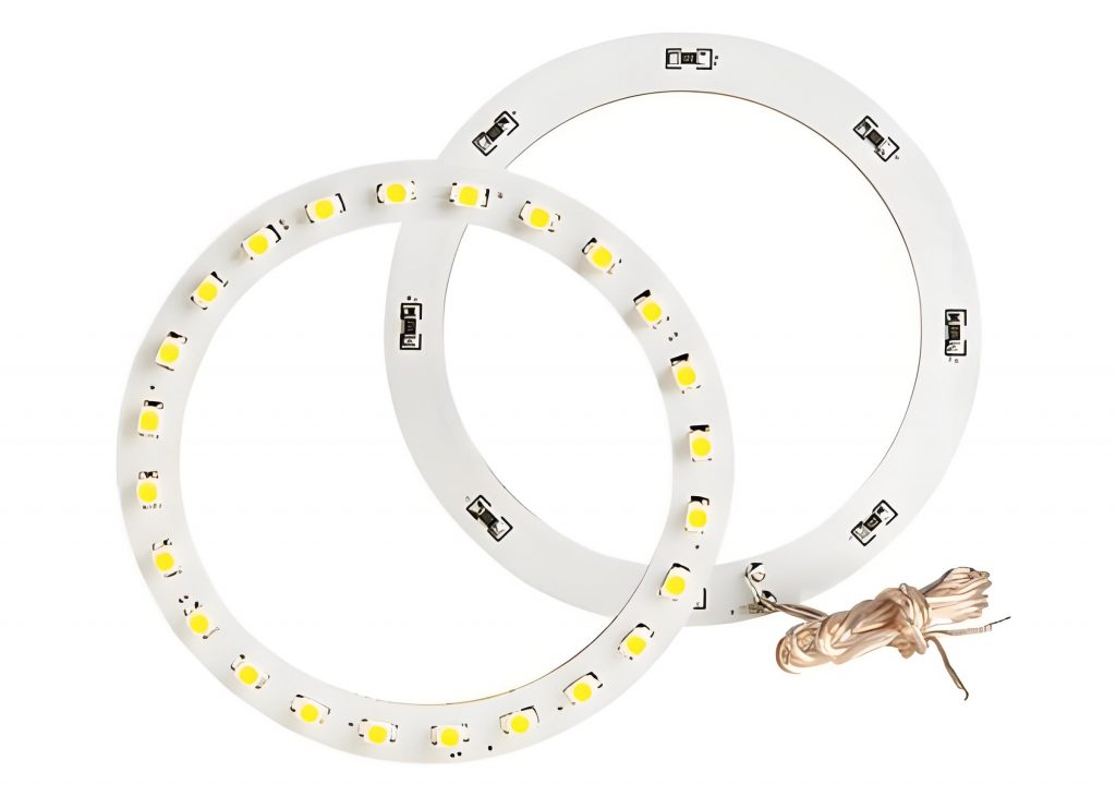
What Is SMD LED PCB Board Design?
SMD LED PCB board design refers to the process of designing printed circuit boards that support Surface Mount Device (SMD) LEDs. These boards are commonly used in lighting applications, display panels, and electronic signage. Unlike through-hole LEDs, SMD LEDs are mounted directly onto the PCB surface, enhancing efficiency and reducing assembly costs.
SMD LED PCB Design Software
Here are common SMD LED PCB design software:
- Altium Designer-Offers comprehensive PCB design tools with 3D visualization.
- KiCad: A free, open-source option for designing SMD LED PCBs.
- EAGLE: User friendly and widely used in hobbyist and professional projects.
- Cadence Allegro: Suitable for High-speed signal design field
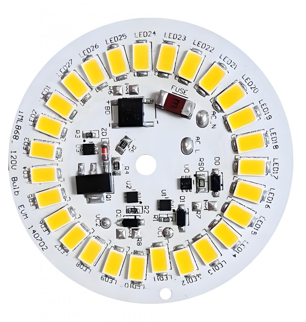
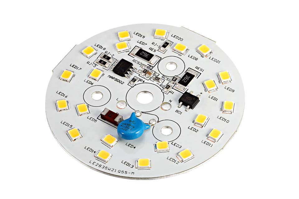
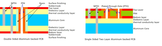
SMD LED PCB Design Layout
The design layout of SMD LED PCBs mainly includes the following aspects:
- Heat dissipation priority: copper is laid in the concentrated area of LED for heat dissipation, away from high-temperature components to avoid heat accumulation.
- Wire optimization: the power line is short and wide to reduce impedance; the signal line and the power line are layered or spaced to prevent interference.
- Uniform arrangement: the LED spacing is consistent, avoiding obstructions to ensure that the light-emitting surface faces the same direction.
- Pad matching: the pad is designed according to the package size to avoid cold soldering; sufficient soldering spacing is reserved.
- Polarity identification: clearly mark the positive and negative poles of the LED to avoid reverse patch; leave debugging marks on the board.
SMD LED PCB Design Layout
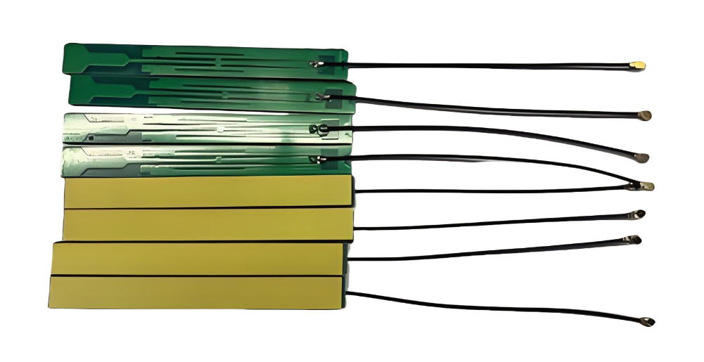
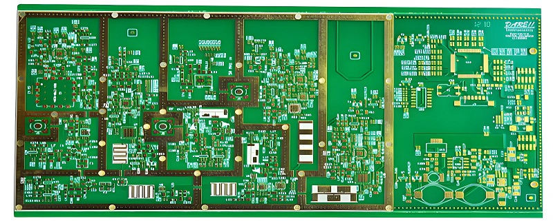
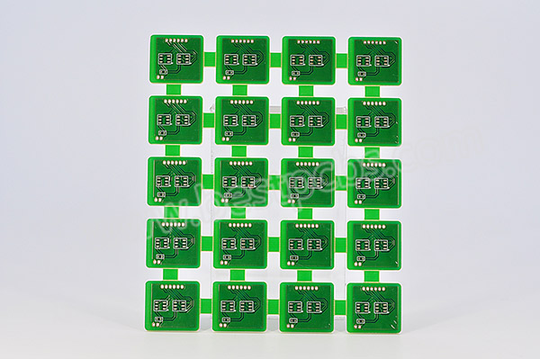
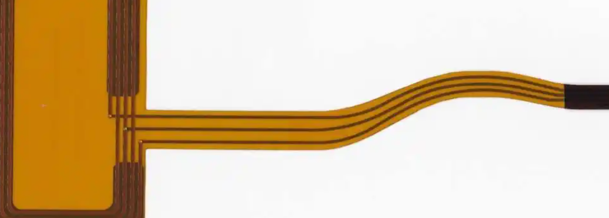
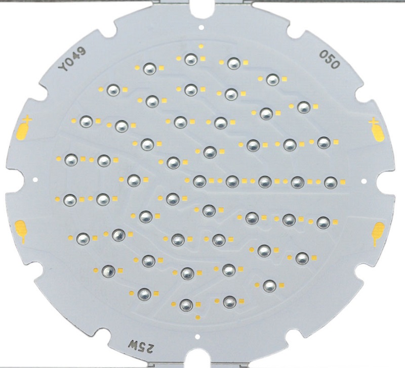
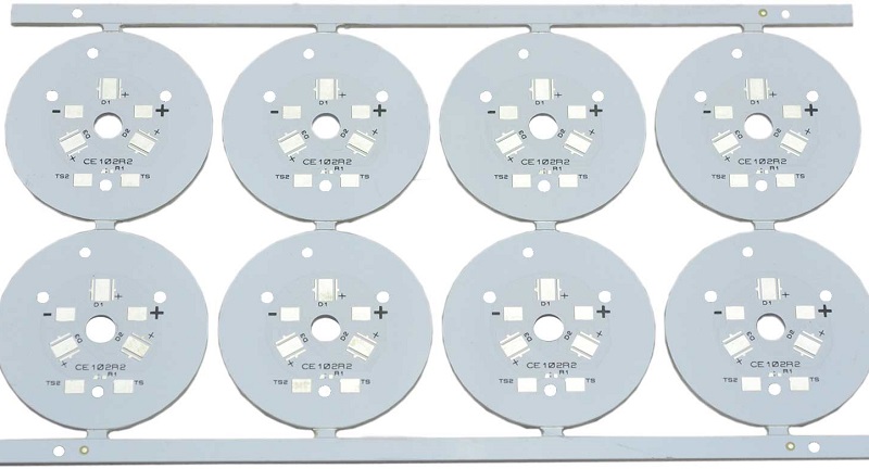
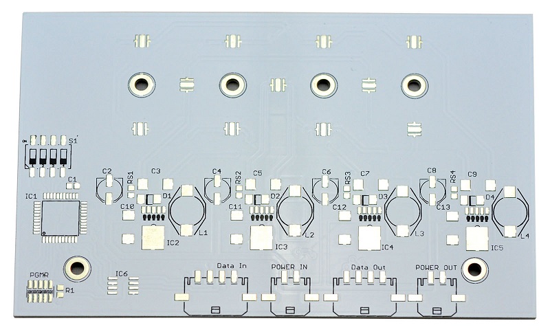
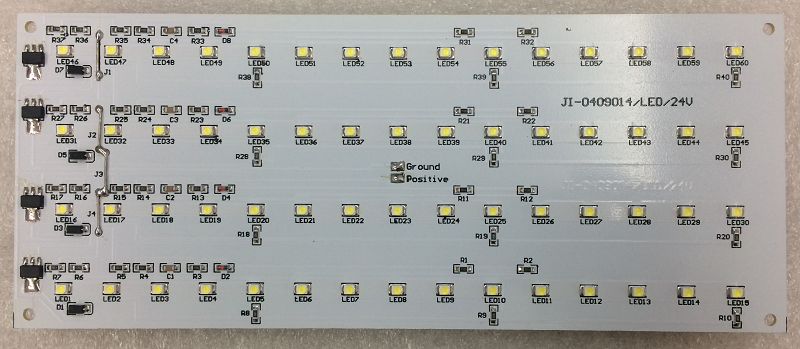
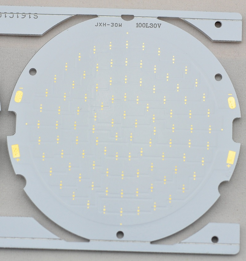
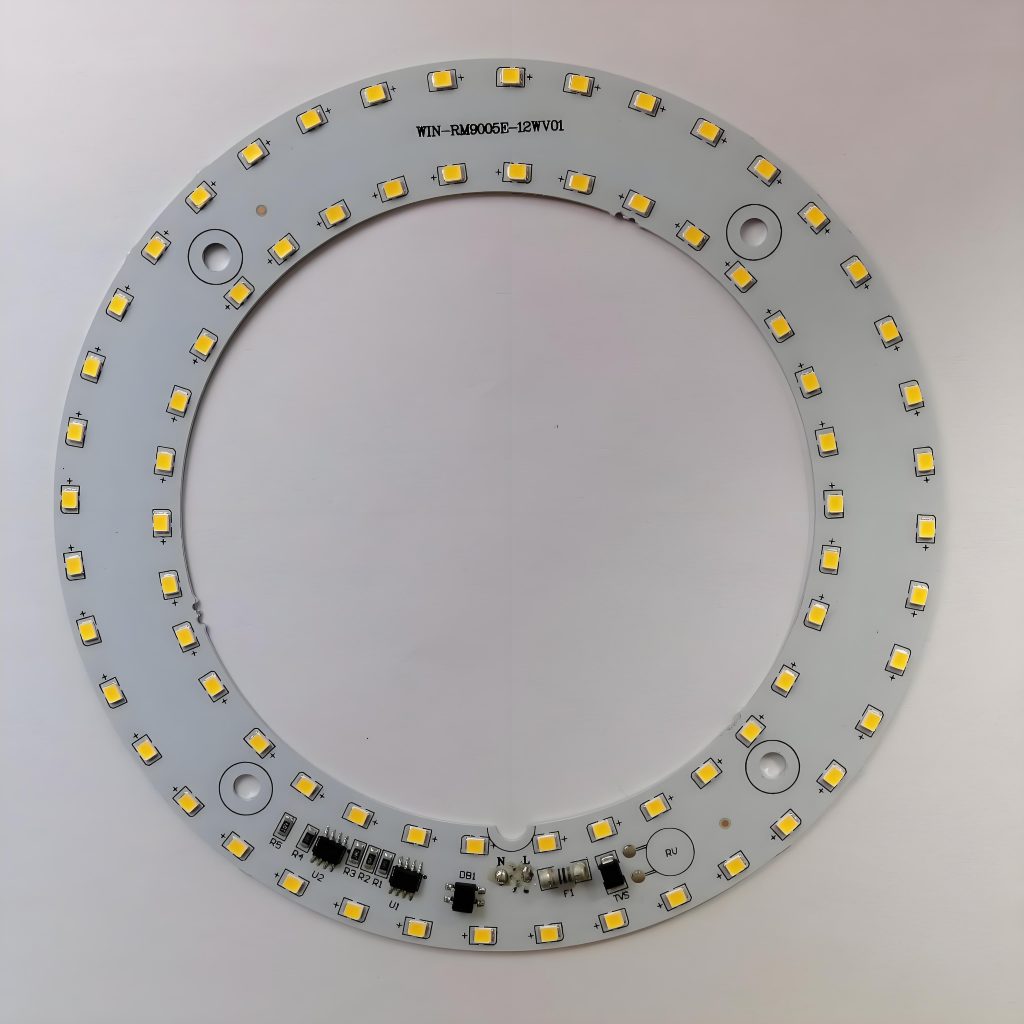
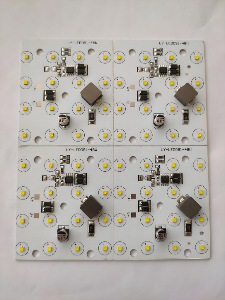
SMD LED Circuit Board Diagram
Here is an example of SMD LED Circuit Board Diagram for reference:
This picture is only for reference, please refer to the actual SMD LED Circuit board design diagram. If you need support on this aspect, please contact us.( the email is at the beginning of this blog)
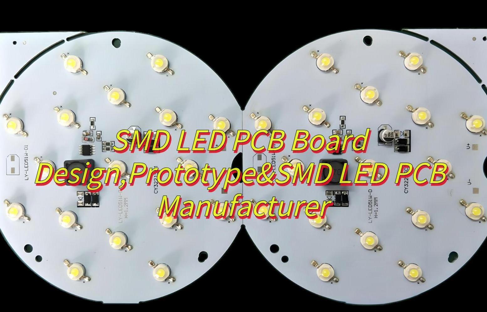
SMD LED PCB Board Manufacturer
When you have finished the design and want to find a SMD LED PCB Board Manufacturer to verify your design. At Best Technology, we can provide affordable prototyping cost with fast delivery, Here are more information about us:
- Focus on SMD LED PCB Board design, prototype and manufacturing over 18 years and have an experienced designers team. We can provide you professional and free technical support quickly.
- Have a complete electronic manufacturing supply chain, providing one-stop solutions and PCBA services. All components you needed we can help you purchase and assemble with PCB.
- Provide PI Analysis, SI Analysis, EMC Testing with the SMD LED PCB you designed.
- Strong process capability
Here is a chart of our process capabilities:
| Base material | Aluminum/Copper/Iron Alloy |
| Thermal Conductivity | 0.8, 1.0, 1.5, 2.0, 3.0 W/m.K. |
| Board Thickness | 0.5mm~3.0mm(0.02″~0.12″) |
| Copper thickness: | 0.5 OZ, 1.0 OZ, 2.0 OZ, 3.0 OZ, up to 10 OZ |
| Outline: | Routing, punching, V-Cut |
| Solder mask: | White/Black/Blue/Green/Red Oil |
| Legend/Silkscreen Color: | Black/White |
| Surface finishing: | Immersion Gold, HASL, OSP |
| Max Panel size: | 600*500mm(23.62″*19.68″) |
| Packing: | Vacuum/Plastic bag |
| Samples L/T: | 4~6 Days |
| MP L/T: | 5~7 Days |
How To Design SMD LED PCB Board?
1. Parameter confirmation and selection
- Single LED operating voltage (such as 3V), current (20mA) and maximum power consumption (power = voltage × current).
- Series/parallel configuration: series voltage superposition (total voltage = single voltage × quantity), parallel connection requires current equalization design.
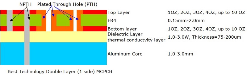
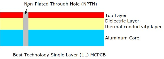
- Materials For general scenario: FR4 board (cost-effective, temperature resistance 130℃).
- Materials For high power scenario: Aluminum substrate (thermal conductivity ≥2.0W/m·K, temperature resistance 150℃).
2. Layout design
- Similar LED spacing rule: ≥0.3mm (to prevent solder bridging).
- Dissimilar device spacing rule: calculated according to the formula 0.13×height difference (mm)+0.3mm (such as LED height 1mm, resistor height 0.5mm, spacing = 0.13×0.5+0.3≈0.365mm).
- All LEDs have the same long axis direction and are perpendicular to the reflow soldering direction (to prevent hot air from causing deviation).
- The distance between the component and the edge of the PCB is ≥3mm. If it cannot be avoided.
- V-Cut board division: Cut after extending the board edge, and wiring is prohibited at the cut.
- Stamp hole board division: Separated by a 0.8mm diameter hole array, the hole center is ≥1.5mm from the board edge
3. Routing and power design
- Line width calculation: Under 1oz copper thickness, line width (mil) = current (A) ÷ 0.024 (such as 1A current requires ≥42mil).
- Copper plating stiffener: The LED negative pad is connected to a large area of copper plating (to reduce impedance and assist heat dissipation).
- Filter capacitor layout: Each LED is connected in parallel with a 0.1μF ceramic capacitor (mounting distance ≤5mm).
- Add 10μF~100μF electrolytic capacitors to the power inlet (to suppress low-frequency ripple).
- Ground plane division: Single-point connection between digital ground and power ground to avoid noise coupling.
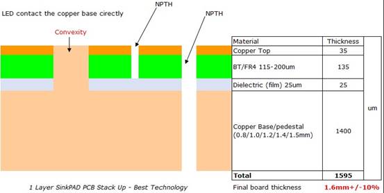
4. Thermal management design
- Heat dissipation hole array: 0.3~0.5mm diameter through holes (1~2mm spacing) are drilled directly below the high-power LED, and the inner wall of the hole is metallized (to enhance thermal conductivity).
- Copper foil area expansion: The copper area under the LED is ≥ 3 times the pad area (the aluminum substrate can be omitted).
- The distance between LED and heating components such as driver IC and MOS tube is ≥ 5mm.
- Avoid arranging electrolytic capacitors in high-temperature areas.
5. Design for manufacturability (DFM)
- Pad design: The pad size is 0.2mm larger than the LED pin (e.g. LED pin is 1.6×0.8mm, and the pad design is 1.8×1.0mm).
- The solder mask opening is 0.05~0.1mm wider than the pad (to prevent the solder mask from covering the pad).
- Polarity mark: Add a “+” symbol or silk screen frame next to the LED pad (to prevent reverse connection).
- Mark point: a solid copper point with a diameter of 1mm is arranged diagonally, and there is no component within 3mm around it.
6. Test and debugging reservation
- Reserve a 30mil diameter circular test point for each LED string circuit (connect to the positive pole of the power supply, ground and dimming signal).
- The test point spacing is ≥2mm to avoid probe short circuit.
- Reserve ≥1.5mm channels in dense LED arrays to facilitate hot air gun rework.
7. Design verification and simulation
- Thermal simulation: Use ANSYS Icepak or similar tools to verify the high temperature area (the temperature rise of the aluminum substrate should be ≤30℃).
- Power integrity simulation: Check the power ripple through Sigrity or HyperLynx (target ≤5% rated voltage).
- DRC inspection: Focus on checking line spacing (≥0.2mm), aperture (≥0.3mm), and pad and through-hole avoidance (≥0.15mm).
8. Production file output
- Gerber file: Contains circuit layer, solder mask layer, silk screen layer, and drilling file (aperture tolerance ±0.05mm).
- Process marking: Clearly specify the solder mask color (white is preferred), surface treatment (immersion gold/OSP), and whether the aluminum substrate needs an insulation layer.
Lastly, you can move the production file to the make a SMD LED PCB board prototype.
What Are SMD LED PCB Board Design Rules?
- Minimum spacing rule: When SMD layout is in progress, ensuring a certain spacing between components can reduce the probability of problems such as cold soldering, bridging, and shadow effects during welding.
- PCB edge requirements: SMD components should not be laid out within 3mm from the two sides of the SMD PCB. This is because the guide groove of the placement machine requires that no components are allowed within 3 to 5mm of the PCB board edge. If this size cannot be guaranteed, consider using V-grooves or stamp holes to lengthen the board, and then remove the excess board after welding.
- Arrangement direction: The arrangement direction of the same components should be as consistent as possible, and a test point with a diameter of 30mil must be left on the same gold track. In addition, the arrangement direction of CHIP, SOT, and SOIC components should be perpendicular to the tinning direction as much as possible to avoid shadow effects.
- Shadow effect: When wave soldering is used, components with large height differences should not be arranged close together to prevent the shadow effect of high components from affecting the soldering of low components.
- Test point requirements: When a right-angle (vertical) arrangement is required, sufficient tinning space must be reserved. The distance of this space should be 0.635mm.
SMD LED PCB Board Design Rules
FAQ of SMD LED PCB Board Design
1. Improper pad design leads to welding defects
- Use “water drop” routing transition to avoid right-angle connection of pads.
- Symmetrically design the pad size to ensure balanced heat capacity on both sides.
2. Insufficient heat dissipation leads to shortened LED life
- Lay a sufficient area of heat dissipation copper foil (≥50mm²/W) under the LED and add heat dissipation through holes.
- Aluminum substrate or metal core PCB is preferred for high-power scenarios.
3. Uneven current distribution of parallel LEDs
- Use star topology wiring to ensure that the length and impedance of each parallel branch are consistent.
- Use constant current driver chip instead of traditional resistor current limiting solution.
4. Process problems caused by overly dense component layout
- Ensure that the LED spacing is ≥0.5mm and is more than 3mm away from the board edge.
- During wave soldering, adjust the LED arrangement direction perpendicular to the tinning direction, and use a stepped steel mesh to control the amount of solder paste.
5. Polarity marking error or silk screen blocking the pad
- Clearly mark the LED polarity (such as the “+” symbol), and keep the silk screen away from the edge of the pad by ≥0.2mm.
- During design verification, check whether the solder mask opening fully exposes the pad.
To sum up, the above is about SMD LED PCB design and how to select a good PCB supplier. If you have any other questions about designing SMD LED PCB, please leave a message below our blog. Looking forward to hearing from you soon!