Thermal conductivity of copper is one of the most important properties of the material, especially in industries like electronics and heat management. With its high thermal conductivity, copper plays a vital role in efficiently transferring heat, making it a go-to material for various applications, including Printed Circuit Boards (PCBs), heat sinks, and cooling systems. But what exactly is the K value of copper, and why should you care? Let’s dive into the fascinating world of copper’s thermal conductivity and how it impacts the way we use this versatile metal.

What is the Thermal Conductivity of Copper?
The thermal conductivity of copper is the measure of how well copper conducts heat. In simpler terms, it defines how easily heat flows through the material. The K value, or thermal conductivity, of copper is exceptionally high, approximately ranging from 380 to 401 W/(m·K), making it one of the most efficient materials for heat transfer. This characteristic is crucial in applications where efficient heat dissipation is required.
The high thermal conductivity of copper means it can quickly absorb and release heat, which is why it’s widely used in applications such as wiring, heat exchangers, and cooling systems. This ability to efficiently manage heat is especially important in electronics and the manufacturing of PCBs.
What Factors Affect the Thermal Conductivity of Copper?
Several factors can influence the thermal conductivity of copper, and understanding them helps optimize copper’s use in various industries.
Temperature: As temperature increases, copper’s thermal conductivity decreases slightly. However, copper still remains highly conductive compared to most other materials, even at higher temperatures. The temperature dependence of copper’s thermal conductivity is relatively low compared to some other materials.
Purity: Pure copper has the highest thermal conductivity. The thermal conductivity of pure copper is approximately 401 W/(m·K). Impurities or alloying elements in copper can reduce its ability to conduct heat. That’s why many applications rely on high-purity copper to ensure optimal thermal performance.
Structure: The microstructure of copper also plays a significant role. For instance, copper that is in a crystalline form tends to have better thermal conductivity compared to non-crystalline forms.
External Conditions: Environmental factors like pressure and surrounding gases can also affect how well copper conducts heat. In controlled environments, copper’s thermal conductivity can perform even better.
What is the Thermal Conductivity of Stainless Steel Compared to Copper?
When comparing copper to stainless steel, the difference in thermal conductivity is striking. Copper outperforms stainless steel by a significant margin. Taking 304 stainless steel as an example, its thermal conductivity is approximately 16 W/(m·K). This makes copper far more efficient at transferring heat, which is one of the reasons why copper is preferred for applications that require quick heat dissipation.
While stainless steel has its own advantages, such as strength and corrosion resistance, its relatively low thermal conductivity means it’s not the best choice for applications that rely on fast heat transfer.
What is the Most Thermally Conductive Metal?
The most thermally conductive metal is actually silver, not copper. Silver has a thermal conductivity of around 429 W/m·K, which is slightly higher than copper. However, due to its cost and less common use, copper is generally preferred in industrial applications. Silver’s high thermal conductivity makes it ideal for specialized applications, but copper provides a more affordable solution without compromising performance in most heat management scenarios.
Is Copper a Good Thermal Conductor?
Absolutely! Copper is renowned for being one of the best thermal conductors. Copper is with High K value, it’s widely used in industries that require efficient heat transfer. Its ability to quickly dissipate heat makes it an excellent material for electronics, cooling systems, and heat exchangers.
In fact, copper’s combination of high thermal conductivity, ductility, and strength makes it a popular choice for various industrial applications. It’s the material of choice when heat management is crucial, and it’s especially valued in the production of PCBs and other components in the electronics industry.
Why is the Thermal Conductivity of Copper Important?
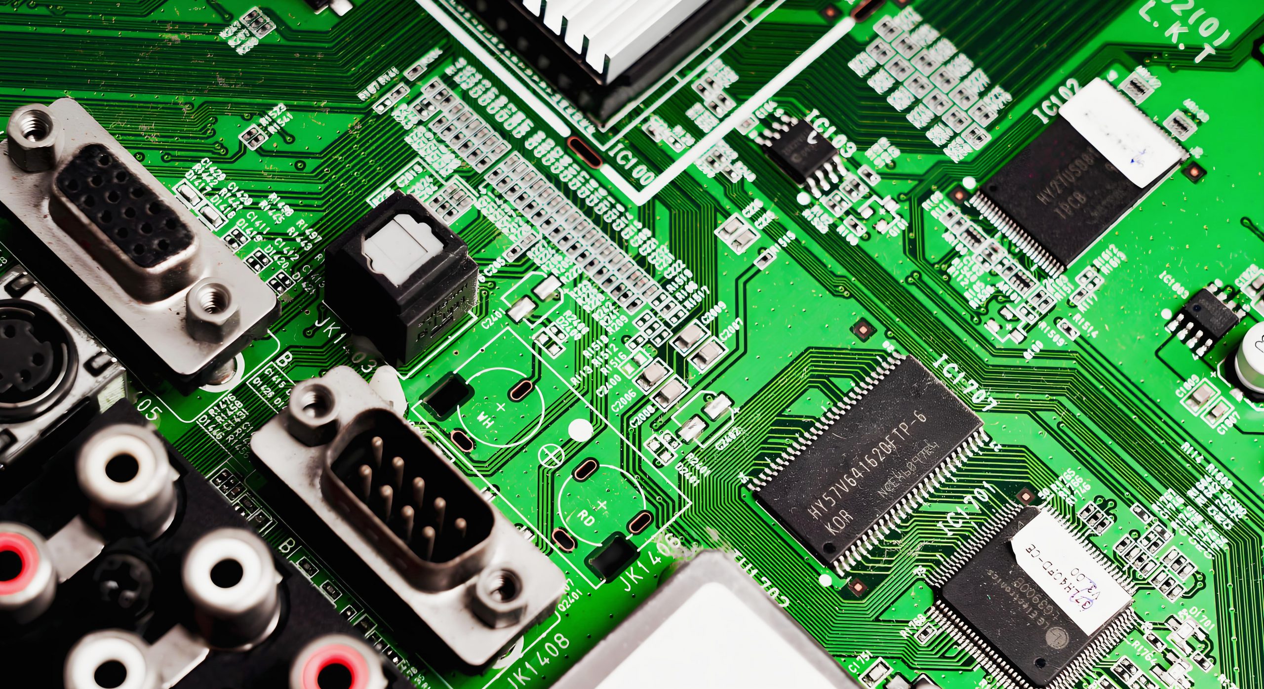
The thermal conductivity of copper is essential because it directly affects the performance of the products that rely on copper for heat dissipation. Whether it’s in electronics, automotive systems, or home appliances, copper’s ability to efficiently transfer heat ensures that components remain within safe operating temperatures, preventing overheating and potential damage.
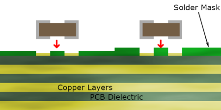
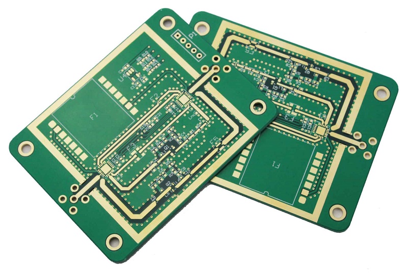
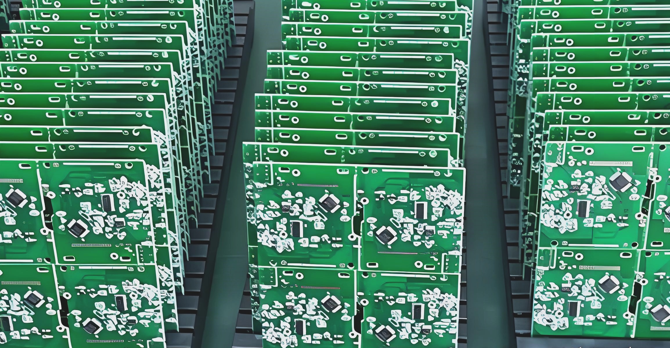
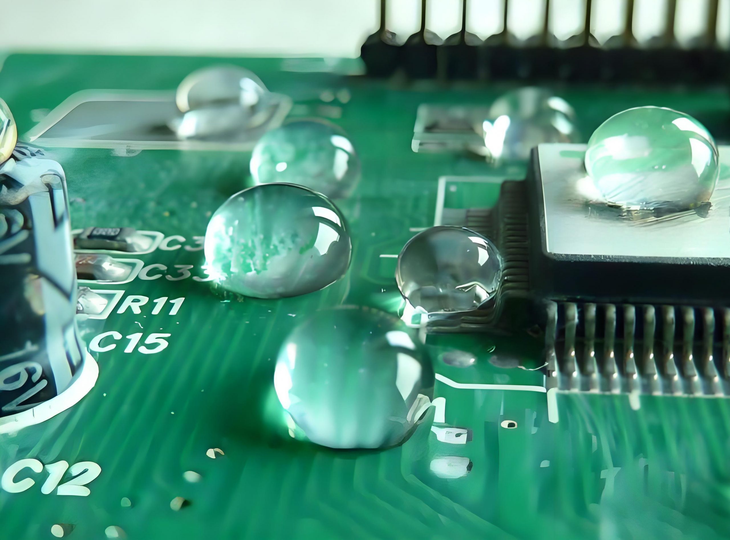
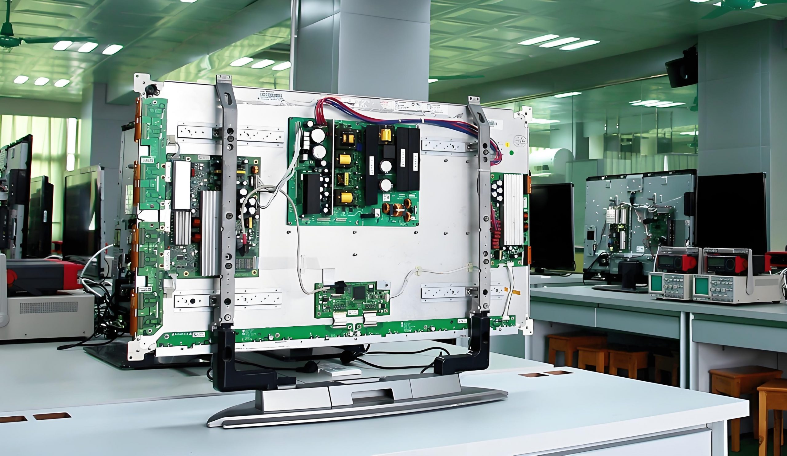
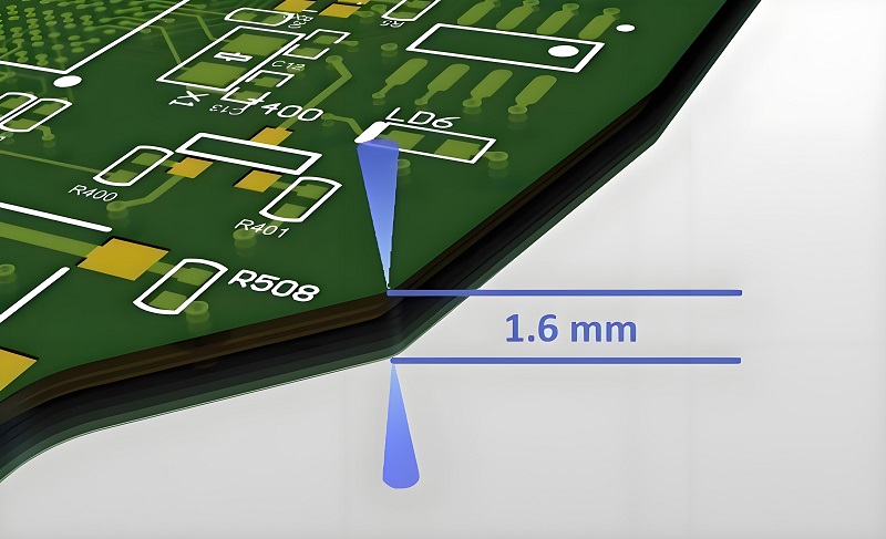
For example, in PCB manufacturing, copper’s thermal conductivity is a critical factor in maintaining the performance and longevity of electronic devices. The better the heat dissipation, the longer the device can run without encountering thermal stress, which can lead to failures.
How Does Copper Compare to Other Heat Sink Materials?
Heat sinks are a crucial part of many electronic devices, and copper is often the material of choice for high-performance heat sinks. When compared to other materials, copper stands out due to its superior thermal conductivity. Aluminum, another popular heat sink material, is also effective but has a thermal conductivity of around 205 W/m·K to 237W/m·K—roughly half that of copper.
This difference means copper heat sinks are better at transferring heat away from critical components, ensuring that electronics maintain optimal temperatures during operation. While aluminum is more affordable and lighter, copper’s superior thermal conductivity makes it the material of choice for applications where performance is critical.
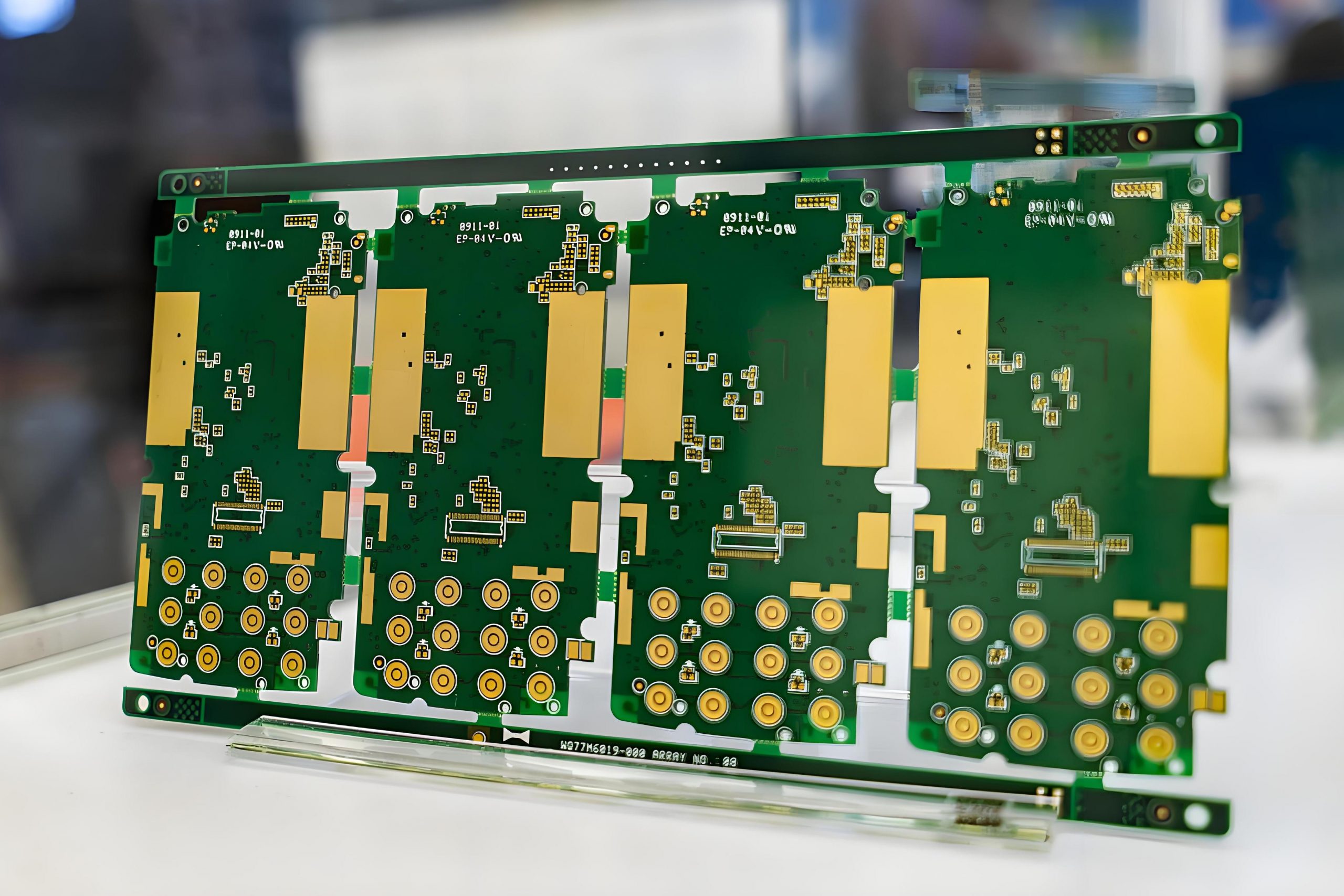
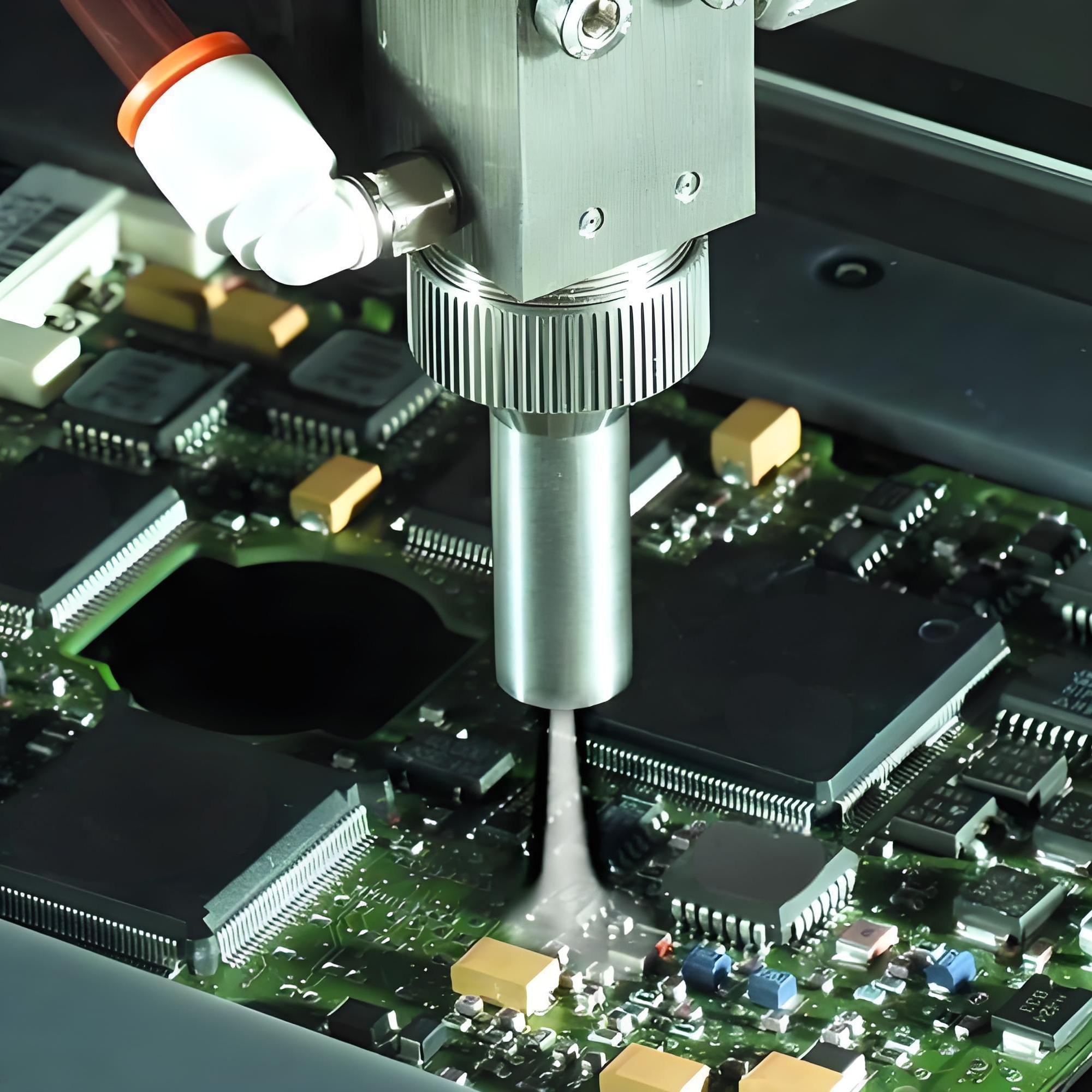
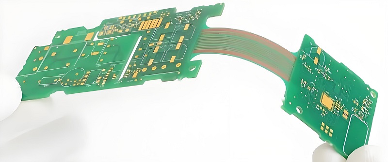
How Does Copper Thermal Conductivity Impact PCB Manufacturing?
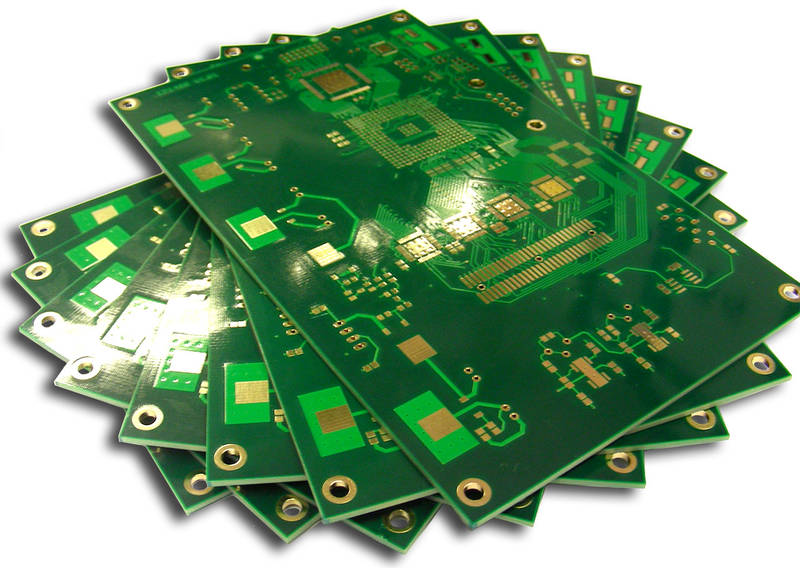
In PCB manufacturing, the thermal conductivity of copper is incredibly important. PCBs used in high-power applications, such as inverters and power supplies, rely on copper to effectively dissipate heat. A copper PCB has superior thermal management properties compared to other materials, ensuring that heat doesn’t build up and cause damage to sensitive components.
Copper’s ability to transfer heat efficiently is one of the reasons it’s widely used in PCB designs. The material helps maintain a safe operating temperature, extending the lifespan of the board and preventing thermal-related failures. Additionally, copper’s high thermal conductivity is essential for ensuring that heat is evenly distributed across the PCB, preventing hot spots that can lead to malfunction.
In many ways, the thermal conductivity of copper directly impacts the performance and reliability of electronic devices, making it a key factor in the PCB manufacturing process.
The thermal conductivity of copper is a critical property that impacts many industries, particularly electronics and PCB manufacturing. Its high K value makes it an ideal material for heat management, ensuring that devices operate efficiently and remain within safe temperature ranges. Understanding copper’s thermal conductivity helps manufacturers optimize their designs for better performance, reliability, and longevity.
As we’ve seen, copper is a good thermal conductor. Whether you’re designing PCBs, heat exchangers, or cooling systems, copper’s thermal conductivity is a key factor in ensuring your products perform at their best.
At Best Technology, we specialize in producing high-quality PCBs that utilize copper’s outstanding thermal conductivity to deliver reliable, long-lasting solutions for your electronic needs. With over 18 years of experience, our expert team is ready to support your projects and provide the best thermal management solutions available. Warm welcome to reach us at sales@bestpcbs.com to get more information and personalized solutions.