pcb
Home > Blog

What is Blank PCB?

October 7th, 2024

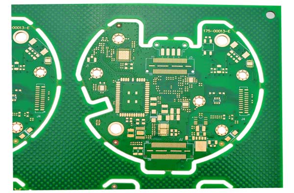
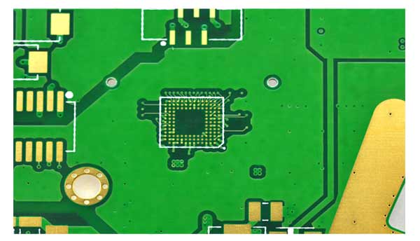
What Is a Blank PCB Called?

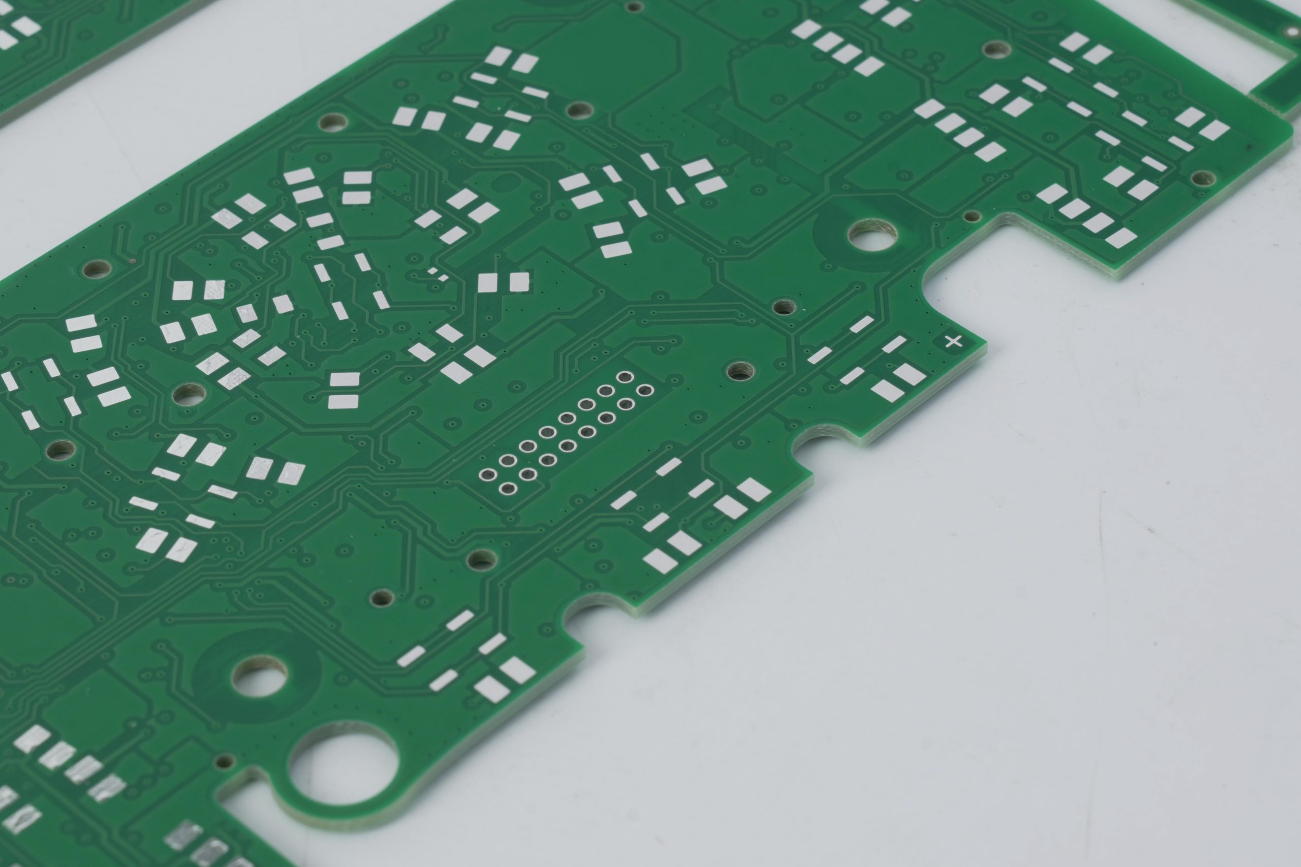
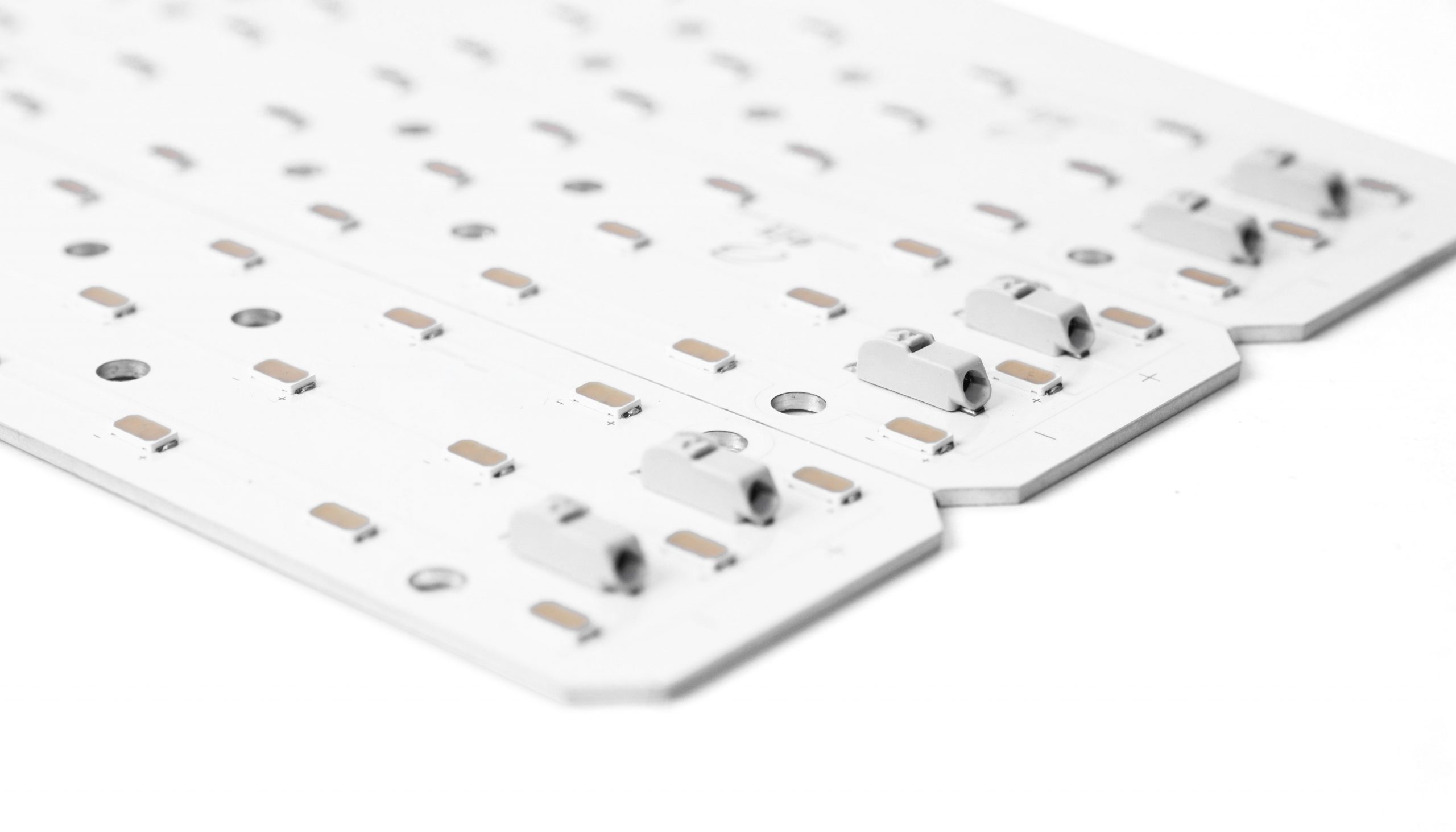
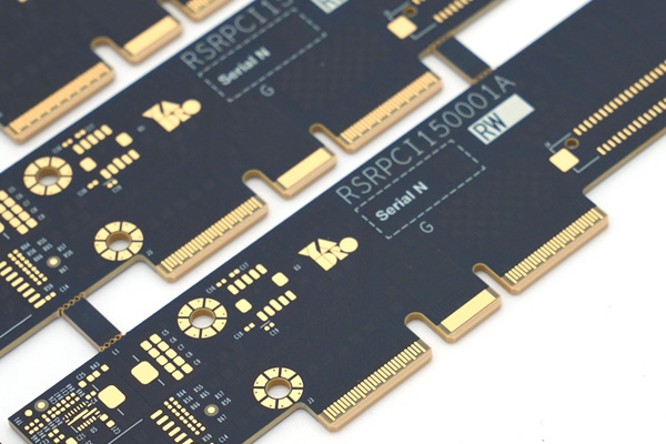
A blank PCB is commonly referred to as a bare board. This term is used because the board has no components soldered onto it yet. Itā€™s simply the foundation of a printed circuit board (PCB), typically made from a material like fiberglass and copper. The copper traces on the board outline where the electrical connections will eventually be made, but before any components are attached, the board remains “blank.”

What is Blank PCB?

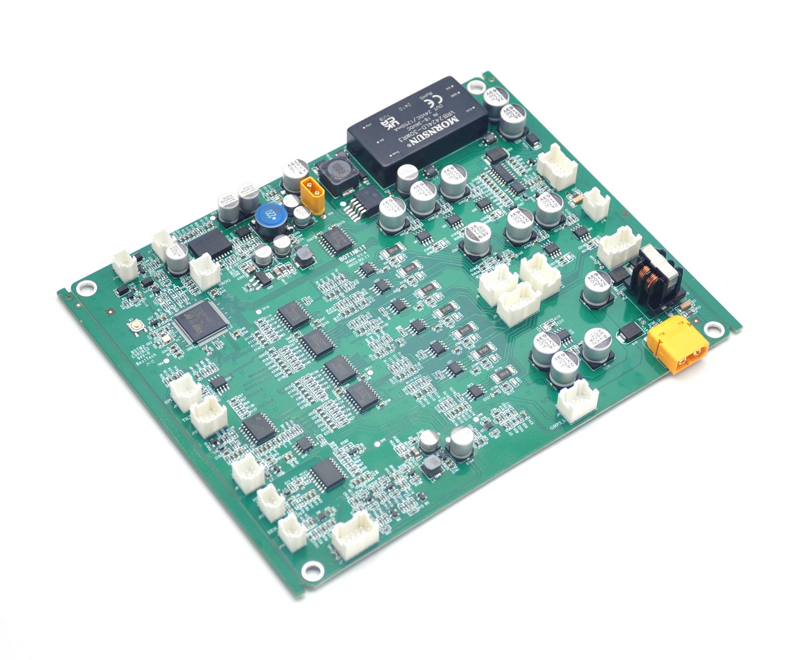
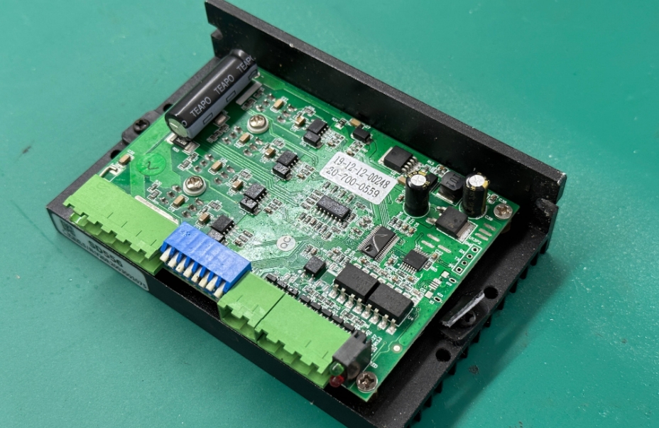
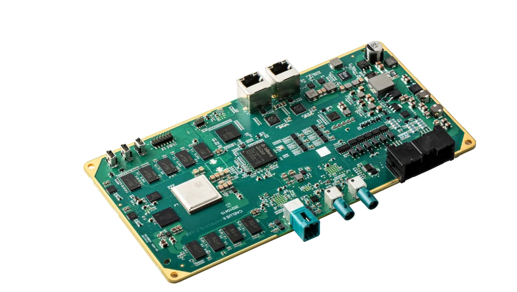
A bare board is key point in the manufacturing process of electronic devices. Once components like resistors, capacitors, and integrated circuits are added, the blank PCB transforms into a fully functional circuit board. This is the stage where the blank board evolves, moving from raw material to the heart of a functioning device.

How to Use a Blank PCB Board?

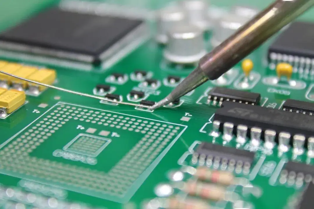
Using a blank PCB starts with designing a circuit schematic. Specialized software is used to create a layout that specifies where each component will be placed and how theyā€™ll be connected through copper traces. Once the design is finalized, the blank board serves as a canvas where components are either soldered by hand or using automated machines in mass production.

If you are working on a DIY project or prototyping, the blank PCB allows for customization and flexibility. You can use a soldering iron to manually attach your components. For large-scale production, automated machines place and solder components onto the blank board with precision. Using blank PCBs for custom designs or modifications is a cost-effective way to experiment with electronics.

Why Is PCB So Cheap?

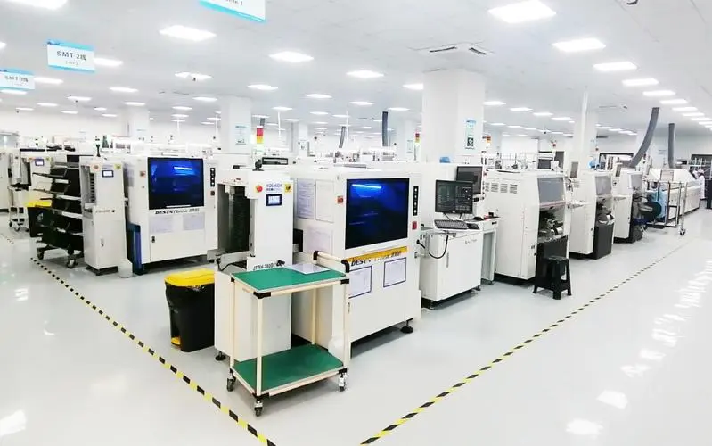
PCBs are considered affordable due to mass production techniques. Modern manufacturing processes, such as automated assembly lines and the use of standard materials, have significantly reduced costs. The global nature of the electronics industry also plays a role, as many manufacturers source materials and labor from countries with lower production costs.

The materials used, primarily fiberglass and copper, are relatively inexpensive. Furthermore, technological advancements have optimized the process of making PCBs, allowing manufacturers to produce them quickly and in large quantities. The result is that even highly specialized PCBs can be produced at a low cost, making them accessible to hobbyists, startups, and large corporations alike. If you want to know the details about factors affect the price of PCB board, welcome to check our another blog:

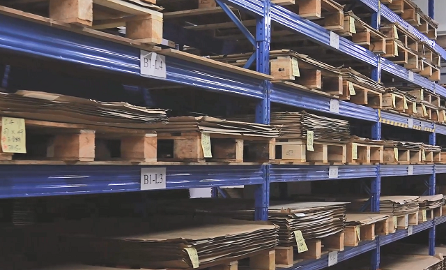
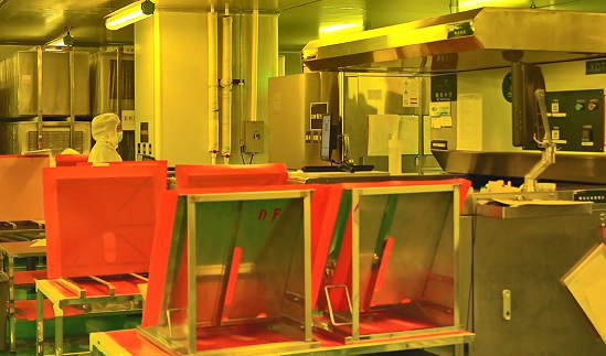
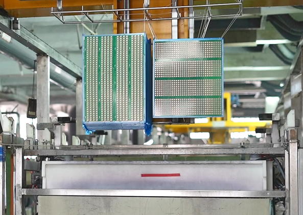
How Are Blank PCBs Made?

The process of making blank PCBs is a sophisticated, multi-stage operation that ensures the boards meet high precision standards before any components are added. Hereā€™s a detailed breakdown of the steps involved in manufacturing a blank PCB:

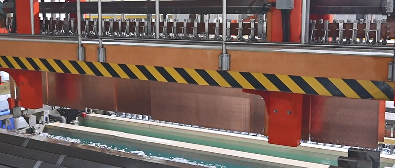
  • Material Selection and Lamination

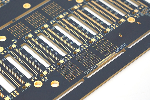
Blank PCBs start with a substrate, typically made from fiberglass-reinforced epoxy laminate (FR4), which serves as the boardā€™s structural foundation. This substrate is non-conductive, providing insulation for the circuit. A copper layer is then bonded to one or both sides of the substrate using heat and pressure, forming what is known as a copper-clad laminate. The thickness of this copper layer varies based on the boardā€™s intended application, with typical copper thickness ranging from 1 oz (35 Āµm) to 2 oz (70 Āµm) per square foot. Thicker copper layers may be used for boards handling higher currents.

What is Blank PCB?
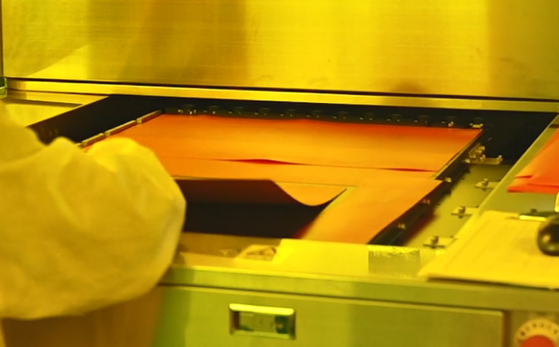
  • Photoresist Application

After lamination, the copper layer is coated with a light-sensitive material called photoresist. This step prepares the board for the next process, which is exposing the circuit pattern. The photoresist layer can be either liquid or dry film and plays a critical role in protecting certain parts of the copper during etching.

What is Blank PCB?
  • Imaging the Circuit Pattern

The desired circuit pattern, generated from PCB design software, is transferred onto the board. This is done by aligning the photoresist-coated board with a photomask (a stencil-like film) that contains the circuit layout. The board is then exposed to ultraviolet (UV) light. The areas of the photoresist not covered by the photomask are hardened, while the areas shielded by the mask remain soft and will later be removed.
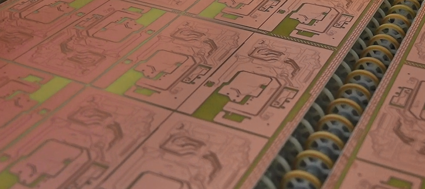
What is Blank PCB?
  • Etching Process

The next step is to remove the unneeded copper from the board, a process called etching. Chemical etchants, like ferric chloride or ammonium persulfate, are used to dissolve the unprotected copper, leaving behind only the circuit traces. The areas of the copper protected by the hardened photoresist remain intact, forming the conductive pathways for the future components.

What is Blank PCB?
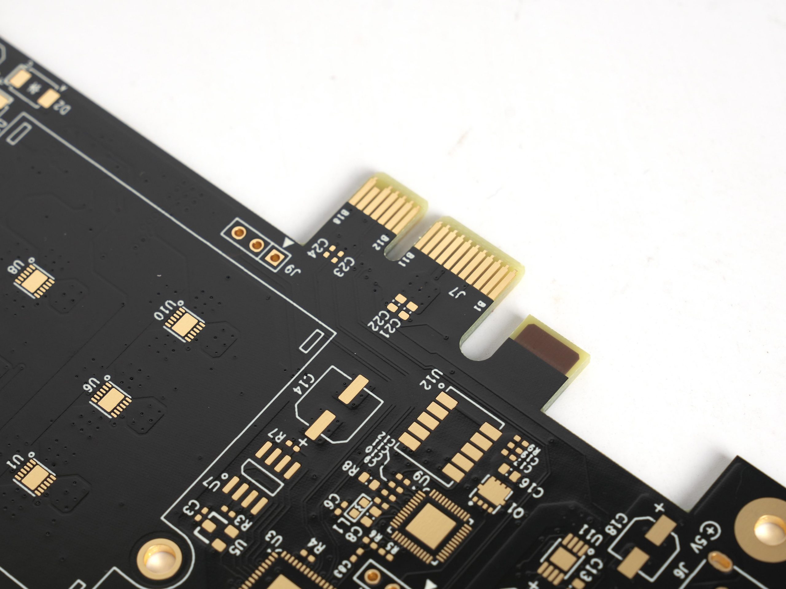
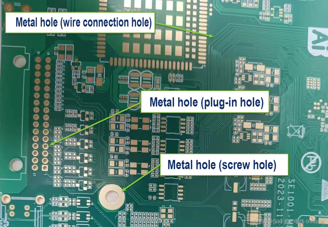
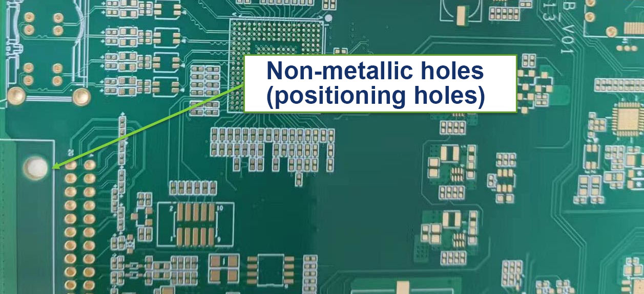
  • Drilling Holes for Components

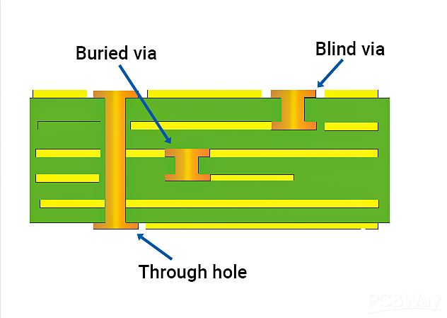
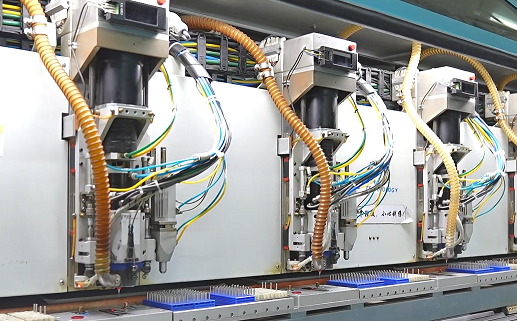
After the etching process, holes need to be drilled into the board. These holes, called vias, allow for the placement of components such as resistors, capacitors, and integrated circuits, and are also used to connect different layers in multi-layer PCBs. Advanced PCB manufacturing often uses computer numerical control (CNC) drilling machines to ensure precision, especially for boards with many layers or small trace designs. Some manufacturers employ laser drilling for microvias.

What is Blank PCB?
  • Plating and Hole Metallization

Once the holes are drilled, they need to be plated to create electrical connections between the different layers of the PCB. This is done through a process called electroless copper plating, which deposits a thin layer of copper inside the drilled holes. The plating process ensures that when components are later inserted, electrical signals can flow between layers through the plated holes.
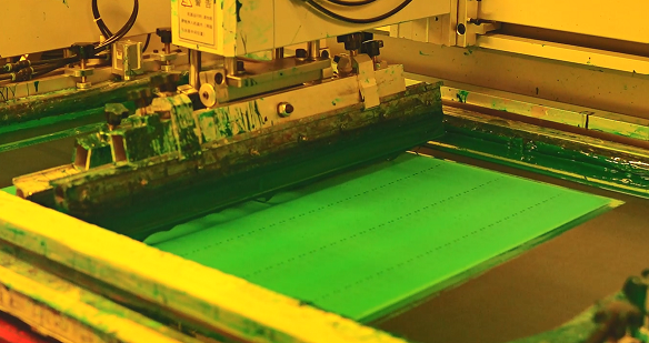
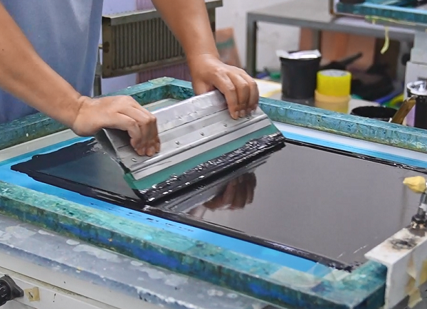
What is Blank PCB?
  • Solder Mask

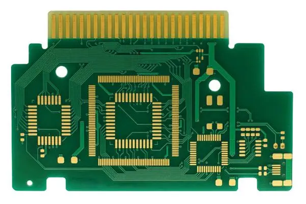
After drilling and plating, the board is cleaned and coated with a layer of solder mask. This mask protects the copper traces and prevents solder from accidentally bridging across traces during assembly. The solder mask is typically green, though other colors like blue, red, black, or white can also be used. The solder mask is applied through a screen-printing process or as a dry film, and it is cured using UV light or heat.

What is Blank PCB?
  • Silkscreen Printing

Silkscreen printing is applied to the board to mark component locations, symbols, logos, or other identifiers needed during the assembly process. This layer is typically applied using a silk-screening process, similar to how images are printed onto clothing. White is the most common color used for silkscreen, as it provides high contrast against the green solder mask, but other colors can be used depending on the design.

What is Blank PCB?
  • Surface Finishing

The copper pads, where components will be soldered later, are treated with a surface finish to protect them from oxidation and ensure good solderability. Common finishes include HASL (Hot Air Solder Leveling), where the board is dipped in molten solder and excess solder is blown off with hot air, leaving a smooth surface. Another popular finish is ENIG (Electroless Nickel Immersion Gold), where a thin layer of nickel followed by gold is applied to the copper pads.

What is Blank PCB?
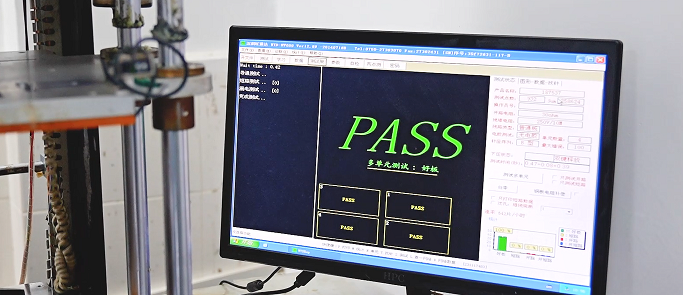
  • Electrical Testing and Quality Control

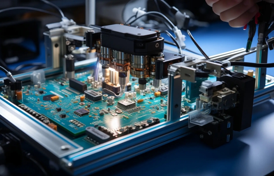
The final step in producing a blank PCB is electrical testing and quality control. Every trace and connection is tested to ensure there are no shorts or opens, which could render the board useless. Automated Optical Inspection (AOI) systems are used to visually inspect the board for defects, while flying probe tests and bed-of-nails tests check for electrical continuity. Any defects found at this stage are flagged for repair or, in severe cases, the board is scrapped.

What is Blank PCB?

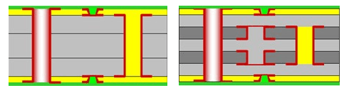
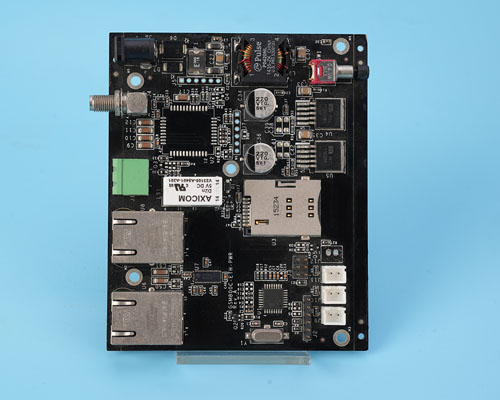
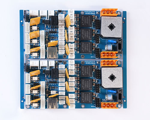
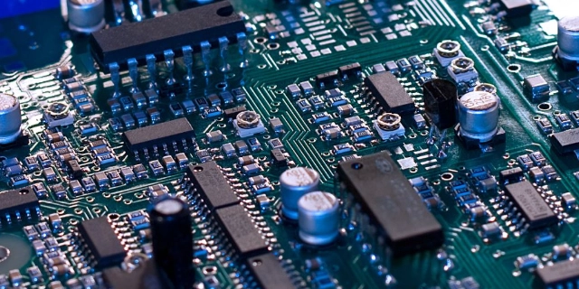
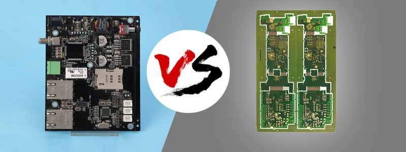
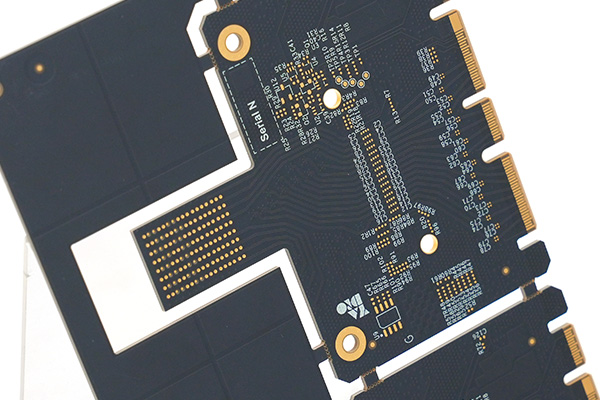
What Is the Difference Between Bare PCB and PCB?

The term bare PCB refers to the unpopulated circuit board, which means it lacks any electronic components. In contrast, a PCB refers to a fully assembled board that includes all the necessary components to function.

In the bare stage, the PCB is simply the foundation for the circuit but isn’t functional. Once components are soldered onto the bare PCB, it becomes an operational printed circuit board, ready to be integrated into electronic devices.

How Do You Cut Blank PCB?

Cutting a blank PCB requires precision. Tools such as PCB shears, laser cutters, or CNC machines are commonly used to achieve clean, straight cuts without damaging the copper traces. For smaller DIY projects, a hand saw or scoring tool can be used, but these methods require a steady hand and careful planning to avoid mistakes.

Before cutting, itā€™s important to mark the board clearly to ensure the cuts are accurate. If the board is part of a larger project, cutting should be done after confirming that all components will fit within the intended space.
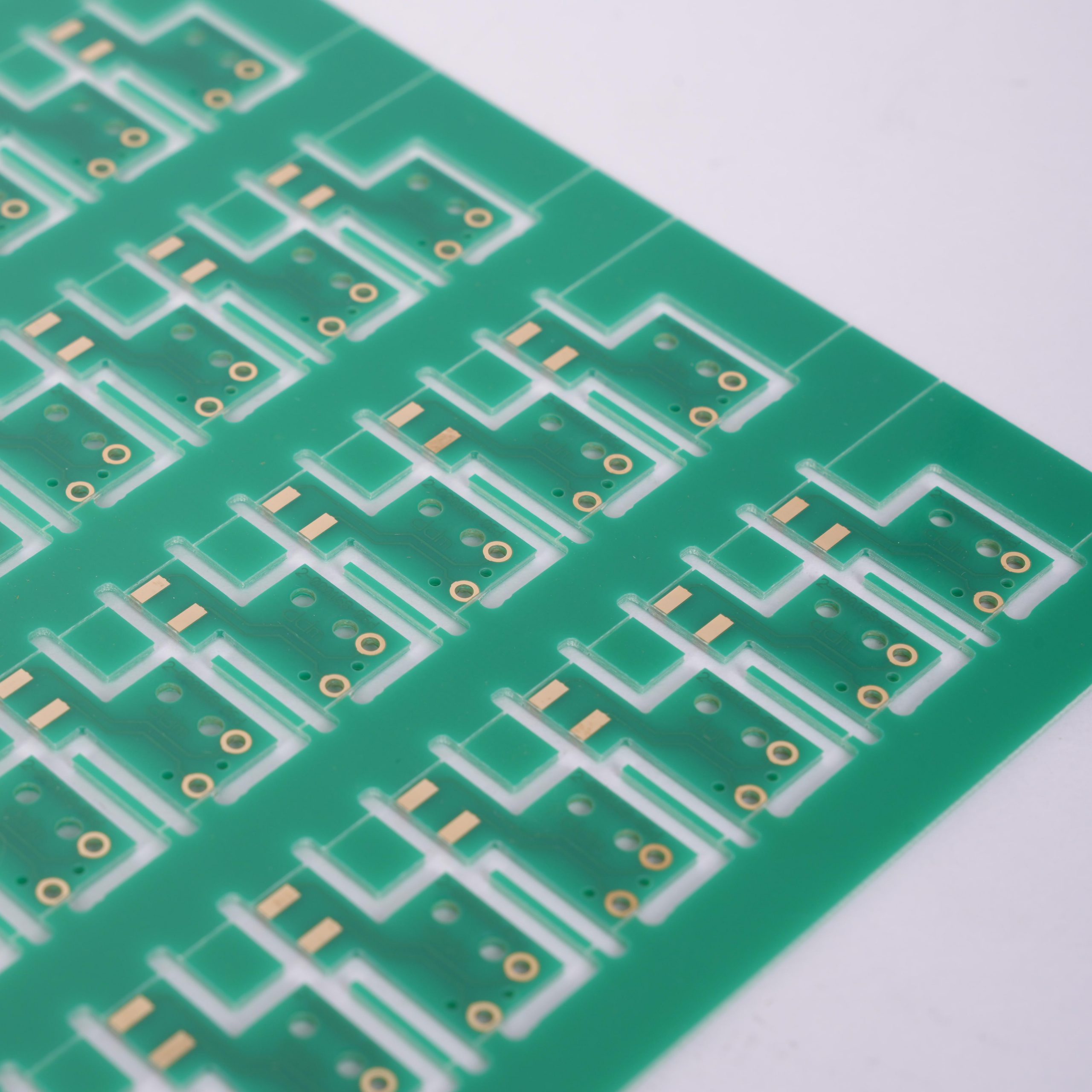
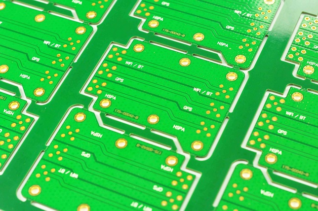
Why Are PCBs Green?

The green color on most PCBs comes from the solder mask that coats the board. While green is the most common color, the solder mask can be found in other colors such as red, blue, or black. The preference for green is largely historical, as it provided the best contrast for technicians to inspect the board visually.

Green solder masks also tend to offer better performance under different lighting conditions, which can be helpful during manufacturing and quality control processes.

Do PCBs Use AC or DC?

PCBs can handle both AC (alternating current) and DC (direct current), depending on the design and the type of components used. Some boards are designed specifically for DC circuits, while others are built to handle AC power.

For example, a power supply PCB may convert AC from a wall outlet into DC, which is used by many electronic devices. The flexibility to work with either type of current makes PCBs essential for a wide range of applications.

Blank PCB Board Supplier ā€“ Best Technology

With over 18 years as an industry leader, Best Technology is one of the most experienced PCB and PCB assembly manufacturer in Asia. We are highly specialized not only in quick-turn PCB prototype and PCB assembly, but also medium and small volume PCB fabrication. In Best Technology, you can enjoy a full-comprehensive one-stop service from PCB design, layout, PCB fabricate, PCB assembly, function testing and delivery. We always try our best to fabricate your PCB with copper clad laminate with the highest quality to meet your demands.

Ā If you have any questions, please feel free to contact us with sales@bestpcbs.com, we will be happy to help you.

What is beveler in pcb?

October 7th, 2024

PCB beveler is a less well-known but very important tool, but it plays a vital role in the manufacturing and assembly process of PCB (printed circuit board). It is a tool specifically used to create bevels or chamfers around the edges or holes of PCB.

What is a PCB Beveler?

PCB beveler is a device used to bevel (chamfer) the edges of printed circuit boards (PCBs). Its functions include improving the electrical performance of PCBs, dispersing the electric field through beveling, reducing the risk of electrical breakdown; enhancing the mechanical properties of PCBs, preventing stress concentration and cracking at the edges; facilitating subsequent processing and assembly work, avoiding scratching other electronic components or damaging component pins during the plug-in process.

What is beveler in pcb?

It has the advantages of high precision, high efficiency, low noise, and low energy consumption. It is widely used in the electronics industry, especially in the production process of consumer electronic products such as smartphones and tablets, which can improve production efficiency and product quality.

What is Edge Bevel in PCB?

Edge bevel is the process of making a transition edge between two sides of a PCB, usually on the outer edge of the PCB. Bevel is often used for edge connectors to allow for smoother insertion into another circuit board socket. Edge connector pins are often called gold fingers because they are plated with gold and have multiple parallel groups together.

Why do PCB edges need to be beveled?

The main reason why PCB edges need to be beveled is to increase the contact area, reduce contact resistance, and improve the stability of electrical connections.

The bevel process increases the contact area between the gold finger and other connectors by processing the PCB edge into a bevel, thereby reducing the contact resistance and improving the stability and reliability of signal transmission.

Specifically, the bevel process has the following advantages in application:

  • ā€ŒIncrease contact areaā€Œ: Beveled edges can increase the contact area between the gold finger and the socket, thereby increasing friction and connection stability.
  • ā€ŒReduce contact resistanceā€Œ: The bevel design reduces the pressure concentration at the contact point, thereby reducing the contact resistance and reducing the loss in signal transmission.
  • ā€ŒAdapt to different application scenariosā€Œ: According to the specific application scenarios and equipment requirements, the bevel angle can be adjusted between 15Ā° and 45Ā° to meet different spatial layouts and electrical connection requirementsā€Œ.

The use of PCB beveling machines further improves the accuracy and efficiency of the beveling process. This mechanical equipment can accurately control the bevel angle through a high-precision mechanical transmission system and an efficient grinding process to ensure processing quality and production efficiency.

What are the Benefits of PCB Edge Beveling?

The main benefits of PCB edge beveling include enhanced aesthetics, easy installation, improved electrical performance, and reduced mechanical stress. ā€Œ

First, the beveling process can enhance the aesthetics of the circuit board. By cutting the PCB edge at a specific angle, the beveling process makes the appearance of the circuit board more refined and beautiful, which can significantly improve the overall visual effect of the productā€Œ.

Secondly, the beveling process is easy to install. The beveling design can better adapt to the structural design of various electronic devices, making the assembly of PCB boards and other components more convenient and precise, and the design of the beveling angle can better achieve the coordination of PCB boards with other componentsā€Œ.

What is beveler in pcb?

In addition, the beveling process can also improve electrical performance. Bevel design can increase the contact area and reduce the contact resistance, thereby improving the stability and reliability of signal transmission.

Finally, bevel design can reduce mechanical stress. The design of the beveled rectangle allows the socket to slowly and gradually enter or exit the jack when plugging and unplugging, thereby reducing the mechanical stress during plugging and unplugging and extending the service life of the socket and jack.

What are the limitations of PCB edge beveling?

The main limitations of PCB edge beveling include the design of the bevel angle, the spacing requirements between the components and the board edge, and the requirements for cutting accuracy and speed. ā€Œ

First, the design of the bevel angle needs to be determined according to the specific application scenario and equipment requirements. The common bevel angle range is between 15Ā° and 45Ā°.

In some devices with high requirements for plugging and unplugging force and contact stability, a smaller bevel angle may be selected to increase the contact area and friction between the gold finger and the socket to ensure the stability of signal transmission; while in some occasions with strict restrictions on spatial layout, a larger bevel angle may be used to better realize the assembly of PCB boards and other components. ā€Œ

Finally, cutting accuracy and speed are also important limiting factors. PCB beveling machines need to have high-precision cutting capabilities and be able to accurately cut within the specified size range. The cutting accuracy directly affects the quality and reliability of the circuit board.

How Does PCB Beveling Work?

PCB beveling machines are usually composed of a frame, a transmission system, a grinding system, a positioning fixture, and a protective device.

The transmission system uses high-precision gears or screw drives to ensure processing accuracy. The grinding system consists of a grinding head and a coolant system, etc., which are used to grind PCB boards. The positioning fixture is used to fix the PCB board to ensure the accuracy and stability of the processing, while the protective device is to protect the safety of the operator.

What is beveler in pcb?

During the operation, first check whether the beveling machine is operating normally. If there is a problem, it needs to be repaired. Then, set the beveling angle according to customer needs or the default 45Ā° angle.

Next, adjust the angle of the gong section and the table, adjust the distance of the steel plate according to the thickness of the board, and use a copper plate of the same thickness to test the knife to ensure that the angle of the bevel of the beveled board meets the requirements.

Finally, the grinding process is carried out through the grinding system. The grinding head rotates at a high speed and applies a certain amount of pressure on the PCB board, thereby processing its edge into a bevel.

What are the Applications of PCB Beveling?

The core application of the PCB beveling process is to increase the contact area and reduce the contact resistance, thereby improving the stability and efficiency of the connection. This process is common in the beveling of gold fingers, especially on devices such as computer memory bars and graphics cards. The bevel design of gold fingers can significantly improve the data transmission speed and reliability.

ā€ŒSpecific application scenariosā€Œ include:

  • ā€ŒComputer memory bars and graphics cardsā€Œ: On these components, the bevel design of gold fingers can not only increase the contact area and reduce the contact resistance, but also prevent oxidation to a certain extent and extend the service life.
What is beveler in pcb?
  • ā€ŒOther communication equipmentā€Œ: In addition to computer memory bars and graphics cards, the beveling process of gold fingers is also used in various devices that communicate through digital signals, such as consumer electronics, smartphones, and smart watches.

In short, the beveler in PCB is a tool specifically used to create bevels or chamfers around the edges or holes of PCBs. It has the functions of improving the reliability of PCB, facilitating assembly and improving appearance. When using the bevel, pay attention to the correct operation method and maintenance to ensure its normal operation and service life.

What is the melting point of PCB solder?

October 7th, 2024

PCB solder plays a vital role in the assembly and function of PCBs. Reliable solder joints must remain intact to prevent components from loosening or falling off the PCB. Solder is the material used to connect the various electronic components on the PCB. Its importance is reflected in several key aspects. Solder ensures that electronic components can be firmly attached to the PCB.

What type of solder for PCB?

The commonly used types of solder for PCB include solder paste, tin bar and tin wire. ā€Œ

  • 1. ā€ŒSolder pasteā€Œ: Mainly used in reflow soldering process. Solder paste consists of tin powder, flux and other additives. Tin powder is usually an alloy of tin and other metals. According to different melting points, solder paste can be divided into three types: low temperature, medium temperature and high temperature; according to different lead content, it can be divided into lead solder paste and lead-free solder paste. Lead-free solder paste gradually replaces lead solder paste to reduce environmental pollutionā€Œ.
What is the melting point of PCB solder?
  • 2. ā€ŒSolder barā€Œ: Mainly used in wave soldering process. Tin bar (solder bar) has excellent antioxidant ability, good fluidity after melting, suitable for wave soldering process, and is widely used in PCBA processing due to its good fluidity and strong solderability.
  • 3. Tin wire: Mainly used in post-soldering process. Similar to tin bar, tin wire is also a kind of welding material, mainly used for manual welding or other occasions where filament solder is required.

In addition, the selection of welding materials also involves the selection of solder alloys. Eutectic alloys are one of the preferred solder alloys because of their low melting point, low welding temperature, small crystal grains, and dense structure, which are conducive to improving the strength of solder joints.

What temperature should solder be for PCB?

The solder temperature of PCB should vary according to different types of components and welding processes. ā€Œā€Œ

For lead-containing PCB boards, the temperature in the preheating stage is usually controlled at 80~120ā„ƒ for 1~3 minutes; the temperature in the insulation stage is 150~180ā„ƒ for 30~60 seconds; the temperature in the reflow stage is 210~240ā„ƒ for 20~40 seconds; the cooling stage speed should be controlled within the range of 4~6ā„ƒ per second. ā€Œ

For lead-free PCB boards, the temperature in the preheating stage is usually controlled at 100~150ā„ƒ, the insulation stage is 180~220ā„ƒ, the reflow stage is 240~260ā„ƒ, and the cooling speed should be controlled within the range of 3~5ā„ƒ per second. ā€Œ

What is the best soldering temperature for PCB? ā€Œ

The best soldering temperature range for PCB is usually between 240 and 280 degrees Celsius. This temperature range is suitable for manual soldering and can ensure the best soldering effect and component reliability. ā€Œ

For different types of welding situations, the temperature requirements are different:

  • 1. Wave soldering: The optimal temperature is 280 degrees Celsius, ensuring that the solder joint temperature is 50 degrees Celsius higher than the melting point of the solder to achieve reliable welding results.
  • 2. Small components (such as resistors and capacitors below 1206, and components with an area of ā€‹ā€‹less than 5 mmĀ²): The recommended temperature is 250 degrees Celsius to prevent damage to the circuit board.
  • 3. Large components: The soldering iron temperature should be set between 350 and 370 degrees Celsius, and the maximum should not exceed 390 degrees Celsius. The welding time should be kept within a few seconds to prevent damage to the pads on the PCB.
  • 4. SMT processing: The recommended manual soldering temperature range is 240 to 280 degrees Celsius. Try to minimize the gap between the set temperature and the actual working temperature to achieve the best welding effect and component reliability.
What is the melting point of PCB solder?

In addition, the precise management of temperature during the welding process is also required to ensure the quality of the solder joints and circuit performance of the PCB board.

  • The preheating stage is very important to reduce the thermal shock during welding. The preheating temperature is usually controlled between 80 and 120 degrees Celsius for 1 to 3 minutes.
  • The insulation stage is to fully melt the components and solder paste on the PCB board. The temperature is usually controlled between 150 and 180 degrees Celsius for 30 to 60 seconds.
  • The cooling stage is to avoid thermal stress caused by rapid cooling. The cooling rate should be controlled to drop between 4 and 6 degrees Celsius per second.

What temperature does PCB solder melt?

The melting temperature of PCB solder depends on the type of solder. The melting temperature of lead solder ranges from 183Ā°C to 217Ā°C, while the melting temperature of lead-free solder is usually between 217Ā°C and 257Ā°C.

What is the melting point of PCB solder?

Lead solder has a lower melting point, usually between 183Ā°C and 217Ā°C. During the reflow process, the preheating temperature of lead solder is controlled at 80Ā°C to 120Ā°C, the holding temperature is 150Ā°C to 180Ā°C, the reflow temperature is 210Ā°C to 240Ā°C, and the cooling rate decreases by 4Ā°C to 6Ā°C per second.

The melting point of lead-free solder is higher, usually between 217Ā°C and 257Ā°C. During the reflow process, the preheating temperature of lead-free solder is controlled at 100Ā°C to 150Ā°C, the holding temperature is 180Ā°C to 220Ā°C, the reflow temperature is 240Ā°C to 260Ā°C, and the cooling rate decreases by 3Ā°C to 5Ā°C per second.

What is the melting point of PCB material?

The melting point of PCB material depends on its specific composition and type, usually between 1064ā„ƒ and 900ā„ƒ. For PCB substrate materials, such as FR-4, its temperature resistance is measured by the Tg value (glass transition temperature). Ordinary FR-4 sheets have lower heat resistance, while high TG FR-4 sheets have better heat resistance and can withstand higher temperatures.

Different types of PCB materials have different melting points and heat resistance. The long-term working temperature of ordinary FR-4 sheets is generally between 130ā„ƒ and 140ā„ƒ, and the instantaneous temperature resistance can reach 150ā„ƒ to 260ā„ƒ. In contrast, PCBs made of special materials such as polyimide can withstand higher temperatures, even up to 280ā„ƒ.

In addition, the surface treatment layer material of the PCB will also affect its heat resistance. For example, the melting point of the gold plating layer depends on the composition of the metal material used.

Which solder is best for PCB?

Choosing a solder suitable for PCB requires comprehensive consideration of multiple factors. The following solders have their own advantages and disadvantages:

  • Tin-silver-copper (SAC) alloy: good mechanical and electrical properties, high reliability, suitable for a variety of welding processes, and environmentally friendly. But the cost is high and the welding process requirements are high.
  • Tin-copper (Sn-Cu) alloy: low cost, good solderability, and environmentally friendly. The disadvantage is that the mechanical properties are slightly worse in high-demand scenarios.

What type of solder should not be used with electronics?

Electronic products should not use strong alkali, rosin grease, coconut oil, and neutral flux as flux. ā€Œ

In the soldering process of electronic products, it is very important to choose a suitable flux. The main function of the flux is to remove the oxide film, prevent oxidation, and improve the quality of soldering.

However, some substances are not suitable for use as flux. Strong alkali and rosin grease will corrode the soldering joint and affect the quality of soldering. In addition, the use of acidic flux will also corrode the soldering joint, so acidic flux should be avoided.

In order to ensure the smooth progress of the soldering process and ensure the quality of soldering, some measures can be taken.

First, choose lead-free solder materials that meet ROHS standards to reduce environmental pollution. Second, use high-brightness soldering iron tips, reduce the use of soldering oil and rosin, and reduce smoke generation. Finally, select appropriate welding materials and processes according to specific needs, such as solder wire, solder paste, solder sheet, etc., to ensure the mechanical and electrical performance of welding.

In short, solder is a key element in the PCB assembly process. Its quality is directly related to whether the electronic equipment can operate normally, and the characteristic of solder melting point plays a decisive role in the welding process. I must deeply study and understand the characteristics of solder to ensure that every solder joint can meet the highest standards.

Can you use AC in PCB?

October 7th, 2024

Can you use AC in PCB?AC can be used in PCB boards. PCB boards are designed to support the use of AC, and the functions of AC can be realized through proper circuit design and component selection.

Can you use AC in PCB?

Can you use AC in PCB?

The use of AC in PCB boards requires consideration of the characteristics of AC. The current magnitude and direction of AC change continuously over time, which requires the components and layout on the PCB to adapt to such changes. For example, components such as inductors and capacitors play an important role in AC circuits, and their parameters and layout need to be carefully designed to achieve the desired circuit performance.

Specifically, AC circuit design on PCB boards includes selecting appropriate components, layout, and routing. For example, using test instruments such as LCR digital bridges can measure the parameters of components in AC circuits to ensure that the performance of the circuit meets the design requirements. In addition, reasonable ground routing and layout can reduce signal interference and ensure the stable transmission of AC.

Is the circuit board DC or AC?

Circuit boards can transmit both direct current and alternating current. In modern electronic products, we use alternating current for power supply, so most circuit boards are also designed to transmit alternating current. Of course, in some special application scenarios, some circuit boards also need to transmit direct current. Whether transmitting direct current or alternating current, the circuit board needs to meet the requirements of the transmitted current.

Is the circuit board DC or AC?

What is the PCB in AC?

The alternating current in PCB refers to the current whose direction changes periodically, that is, alternating current (AC). The application of alternating current in PCB is mainly reflected in power conversion and power transmission. PCB power supply usually converts AC into stable direct current (DC) output to meet the demand of electronic equipment for stable power supply. PCB power supply converts AC into the required DC through components such as transformers, rectifiers, filters and voltage regulators, and provides stable power output.

How to calculate the bandwidth of AC in PCB traces

The calculation of AC PCB trace width can be performed by the following formula: W = (I / J) * K, where W represents the trace width, I represents the current, J represents the current density, and K represents a coefficient related to materials and processes. ā€ŒThis formula shows that the trace width is related to the current, current density, and material propertiesā€Œ.

AC in PCB Design Guide

AC in PCB Design Guide

Current Carrying Capacity: The width of a trace directly affects its ability to handle current without exceeding temperature limits or causing excessive voltage drop.
ā€ŒImpedance Control: In high-frequency applications, maintaining controlled impedance is critical for signal integrity. Trace width, trace spacing, and dielectric properties affect the characteristic impedance of the transmission line.
ā€ŒHeat Dissipation: Adequate trace width helps to effectively dissipate heat, preventing thermal issues such as trace delamination or solder joint failure.
ā€ŒVoltage Drop: Narrower traces exhibit higher resistance, resulting in increased voltage drop along the length of the trace. By adjusting the trace width, the voltage drop can be minimized.
ā€ŒManufacturability: The PCB manufacturing process imposes restrictions on the minimum trace width, and designers must balance performance requirements with manufacturability constraints. ā€Œ2.
ā€ŒMinimum Trace Width: Most manufacturers have a minimum trace width of 6mil or 0.152mm, and typically use traces of 0.254-0.3mm.
ā€ŒMaterial and Process Deviations: Due to the possibility of material and process deviations in the actual PCB manufacturing process, a certain margin needs to be left when calculating the line width.
ā€ŒSignal Integrity Simulationā€Œ: Perform signal integrity simulations to ensure impedance is controlled and signal degradation due to reflections, crosstalk, or transmission line effects is minimizedā€Œ

AC in PCB wiring

The current trend is that the power supply voltage is getting lower and lower (especially for highly integrated digital devices), the space occupied is getting smaller and smaller, the weight is getting lighter and lighter, and the efficiency is getting higher and higher, which requires the precise design of the power supply circuit starting from the PCB.

AC in PCB wiring

Safety distance includes electrical clearance (spatial distance), creepage distance (surface distance) and insulation penetration distanceā€¦

  1. Electrical clearance: the shortest distance between two adjacent conductors or one conductor and the adjacent motor housing surface measured along the air.
  2. Creepage distance: the shortest distance between two adjacent conductors or one conductor and the adjacent motor housing surface measured along the insulation surface.

Determination of electrical clearance:

The distance can be determined according to the measured working voltage and insulation level

The electrical clearance size requirements of the primary side line are shown in Table 3 and Table 4

The electrical clearance size requirements of the secondary side line are shown in Table 5

But usually: Primary side AC part: L-N ā‰„ 2.5mm before the fuse, L.N PE (earth) ā‰„ 2.5mm, no requirements are made after the fuse is installed, but a certain distance should be maintained as much as possible to avoid short circuit damage to the power supply.

Primary side AC to DC part ā‰„2.0mm

Primary side DC ground to earth ā‰„2.5mm (primary side floating ground to earth)

Primary side to secondary side ā‰„4.0mm, components connected between primary and secondary sides

Secondary side gap ā‰„0.5mm

Secondary side ground to earth ā‰„1.0mm

Note: Before determining whether it meets the requirements, the internal parts should be applied with a force of 10N and the outer shell with a force of 30N to reduce the distance so that the space distance still meets the requirements under the worst case.

Determination of creepage distance:

Based on the working voltage and insulation level, the creepage distance can be determined by looking up Table 6

But usually: (1), primary side AC part: L-N ā‰„2.5mm before the fuse, L.N earth ā‰„2.5mm, no requirement is required after the fuse, but try to keep a certain distance to avoid short circuit damage to the power supply.

(2) Primary side AC to DC part ā‰„2.0mm

(3) Primary side DC ground to ground ā‰„4.0mm such as primary side ground to earth

(4) Primary side to secondary side ā‰„6.4mm, such as optocoupler, Y capacitor and other components, the foot spacing ā‰¤6.4mm needs to be slotted.

(5) Secondary side parts ā‰„0.5mm

(6) Secondary side ground to earth ā‰„2.0mm or more

(7) Transformer two-stage ā‰„8.0mm or more

  1. Insulation penetration distance:

It should meet the following requirements according to the working voltage and insulation application:

  • For working voltage not exceeding 50V (71V AC peak or DC value), there is no thickness requirement;
  • The minimum thickness of additional insulation should be 0.4mm;
  • When the reinforced insulation is not subjected to any mechanical stress that may cause deformation or performance degradation of the insulating material at normal temperature, the minimum thickness of the reinforced insulation should be 0.4mm. If the insulation provided is used in the protective casing of the equipment and will not be bumped or scratched during maintenance by the operator, and any of the following conditions apply, the above requirements do not apply to thin insulating materials regardless of their thickness;
  • For additional insulation, at least two layers of material are used, each of which can pass the dielectric strength test for additional insulation; or:
  • For additional insulation composed of three layers of material, any combination of two layers of material can pass the dielectric strength test for additional insulation; or:
  • For reinforced insulation, at least two layers of material are used, each of which can pass the dielectric strength test for reinforced insulation; or:
  • For reinforced insulation composed of three layers of insulating material, any combination of two layers of material can pass the dielectric strength test for reinforced insulation.
  1. Points to note about wiring process:

Flat components such as capacitors must be flat without glue.

If the distance between two conductors can be shortened by applying a force of 10N, which is less than the safety distance requirement, glue can be used to fix the part to ensure its electrical clearance.

When laying PVC film inside some shell equipment, attention should be paid to ensuring the safety distance (pay attention to the processing technology).

When fixing the parts with glue, be careful not to leave foreign matter such as glue wire on the PCB board.

When processing parts, insulation damage should not be caused.

  1. Requirements for flame-proof materials:

Heat shrink tubing V-1 or VTM-2 or above; PVC tubing V-1 or VTM-2 or above

Teflon tubing V-1 or VTM-2 or above; plastic materials such as silicone sheets, insulating tape V-1 or VTM-2 or above

PCB board 94V-1 or above

  1. Regarding insulation level

(1) Working insulation: insulation required for normal operation of equipment

(2) Basic insulation: insulation that provides basic protection against electric shock

(3) Supplementary insulation: independent insulation applied in addition to basic insulation to protect against electric shock in case of basic insulation failure

(4) Double insulation: insulation consisting of basic insulation plus supplementary insulation

(5) Reinforced insulation: a single insulation structure that provides the same level of protection against electric shock as double insulation under the conditions specified in this standard

The applicable situations of various insulation are as follows:

A. Operational insulation

a. Between parts with different voltages

b. Between ELV circuits (or SELV circuits) and grounded conductive parts.

B. Basic insulation

a. Between parts with dangerous voltages and grounded conductive parts;

b. Between SELV circuits with dangerous voltages and grounding-dependent;

c. Between the primary power conductor and the grounded shield or the core of the main power transformer;

d. As part of double insulation.

C. Supplementary insulation.

a. Generally speaking, between accessible conductive parts and parts that may carry dangerous voltages after basic insulation is damaged, such as:

ā… . Between the surface of handles, knobs, handles or similar objects and their ungrounded axis.

ā…”. Between the metal casing of the second category equipment and the outer skin of the power cord passing through this casing.

ā…¢. Between the ELV circuit and the ungrounded metal casing.

b. As part of double insulation

D. Double insulation

Double insulation Reinforced insulation

Generally speaking, between the primary circuit and

a. between accessible ungrounded conductive parts, or

b. between floating SELV circuits, or

c. between TNV circuits

Double insulation = basic insulation + supplementary insulation

Note: ELV circuit: extra low voltage circuit

Under normal working conditions, the AC peak value between conductors or between any conductors does not exceed 42.4V or the DC value does not exceed 60V.

SELV circuit: safety extra low voltage circuit.

A properly designed and protected secondary circuit so that under normal conditions or single fault conditions, the voltage between any two accessible parts, and between any accessible parts and the protective grounding terminal of the equipment (only for Class I equipment) will not exceed the safety value.

TNV: communication network voltage circuit

Under normal working conditions, the circuit carrying communication signals

Difference between direct current and alternating current

ā€ŒThe main differences between DC and AC include direction and polarity, voltage change, current loss, transformer use, and application scenarios.

ā€ŒDirection and polarity:

DC: The direction of the current remains unchanged, and the electrons flow from the positive electrode to the negative electrode.

AC: The direction of the current changes periodically, and the electrons flow back and forth between the positive and negative electrodes. ā€Œ
ā€ŒVoltage change:

DC: The voltage remains constant and does not change over time.

AC: The voltage magnitude and direction change periodically over time. For example, the mains is an AC with a sine waveform.

ā€ŒCurrent loss:

DC: Fault losses are relatively small.

AC: There is capacitive current, and there is capacitive current in the transmission line. ā€Œ
ā€ŒTransformer use:

DC: The voltage cannot be changed using a transformer.

AC: The voltage can be changed using a transformer, which is suitable for boosting voltage to reduce losses during long-distance transportation.

ā€ŒApplication scenarios:

DC: Suitable for low-voltage electrical appliances and occasions that require stable current.
ā€ŒAlternating currentā€Œ: Suitable for household and industrial use, using transformers to change voltage to suit different needs.ā€Œ

FAQ About AC in PCB

FAQ About AC in PCB

FAQ About AC in PCB

Q: The relationship between PCB current and line width. Is the current divided into AC or DC?
A: The relationship between PCB current and line width is not divided into AC or DC. In terms of the nature of the lines on the PCB, the lines are all made of copper materials, and both AC and DC can pass. However, how much current can pass depends on the cross-sectional area of ā€‹ā€‹the line on your PCB. That is, line width x thickness of the copper foil of the line. If the cross-sectional area of ā€‹ā€‹the line is small, only small current signals can pass, and if the cross-sectional area is large, large current signals can pass. This signal can be AC ā€‹ā€‹or DC.
Not just 1mm, any line width can pass DC or AC signals.

Q: There is a packaged device, and there are 2 pins in the device that need to be connected to the live wire and neutral wire of 220V AC respectively. So how to deal with this power line when drawing the PCB? Are there any size requirements for pads, wires, etc.? Are there any protective measures required? Is it not possible to directly add pads to connect to the pin pads of the device?
A: It is best to mill a groove between the neutral wire and the live wire, and choose the thickness of the wire according to the current. When the current is large, you can put a tin layer on the wire, and the pad should be slightly larger.

Q: The grounding of the PCB circuit board design is also the negative pole. What is the difference between the grounding here and the AC grounding?

A: The concept of the circuit board ground is somewhat different from that of the power supply system. The power supply system refers to the earth, that is, the terminal with the same potential as the earth.

The ground in the circuit board is just a common terminal of a potential, which can be positive or negative, depending on the needs of the designer. It’s just that everyone is used to and assumes that the negative pole is the common terminal, that is, the ground. The circuit board ground is not necessarily connected to the earth.

But it must be connected to the earth when EMI filtering is required.

Q: Should all GNDs on the PCB board be connected? There is a terminal (screw type) with two terminals marked as V1+ and V1- on the PCB schematic. Should V1- be connected to the power supply ground? But I used a multimeter to measure why V3- is not connected to other GNDs on the board?

So how do you connect the ground and 10V of the power supply to the V1+ and V1- ends of the terminal?

A: Not all ground wires on the board are connected together. The ground wires are divided into analog ground and digital ground, just like the ground wire in DC and the ground wire in AC cannot be connected together. That is to say, there is a ground wire that is specifically used for power supply, and there is a ground wire that is specifically used for signals (shielding signal interference). These two ground wires cannot be connected together.
In addition, you mentioned V1+ and V1-, and V1- should not be considered a ground wire. Generally, the signal represented by this method is a differential signal, that is, the V1 signal is differentially divided into V1+ and V1-, which can reduce external interference and transmit farther. Finally, V1+ and V1- are integrated into the V1 signal.
You need to figure out whether the V1+ and V1- of the terminal are used for power supply. If they are used for power supply, then V1+ is the positive pole. V1- is the negative pole. Since you didn’t show us the picture, you can’t just connect it randomly. The circuit board needs to connect not only power but also signals, depending on how your board is made.

What is the thermal conductivity of aluminum?

October 4th, 2024

Aluminum is ubiquitous in all kinds of materials in daily life. The thermal conductivity of aluminum plays a very critical role in the wide application of aluminum materials. Whether it is to help electronic devices dissipate heat or to play the advantages of thermal conduction in fields such as automobiles and buildings, the thermal conductivity of aluminum must be considered.

How good is aluminum at conducting heat?

Aluminum has relatively good thermal conductivity, but its thermal conductivity is not as good as copper. The thermal conductivity of aluminum is about 237 W/mĀ·K, while the thermal conductivity of copper is about 385 W/mĀ·K, which means that under the same conditions, copper can transfer heat more efficiently.

What is the thermal conductivity of aluminum?

The reason why aluminum has good thermal conductivity is that its thermal conductivity is high, and aluminum has a high specific heat capacity. Specific heat capacity refers to the amount of heat that needs to be absorbed or released by a unit mass of a substance to increase or decrease the temperature by 1K. Aluminum’s high specific heat capacity makes it more efficient in absorbing and releasing heat, which is crucial for applications that need to dissipate heat quickly.

What is thermal conductivity?

Thermal conductivity is a physical quantity that represents the ability of a material to conduct heat. The higher the thermal conductivity, the less heat is lost within the material. Thermal conductivity is defined as the amount of heat directly conducted through a material per unit cross-section and length per unit temperature difference and per unit time, and is expressed in Watts per meter Kelvin (W/m-K).

What is the thermal heat conductivity of aluminium?

The thermal conductivity of aluminium is 237W/mK. Thermal conductivity (k) is a measure of the ability of heat to flow through a material.

Thermal conductivity (k) is a measure of the ability of a material to conduct heat, and represents the amount of heat flow through a unit area per unit temperature gradient per unit time. Aluminium, as a common metal material, has a high thermal conductivity and is suitable for applications that require good thermal conductivity.

What is the thermal conductivity of aluminum?

What is the thermal conductivity of aluminium at high temperatures?

The thermal conductivity of aluminium changes as the temperature increases. Generally speaking, as a metal gets hotter, its thermal conductivity decreases slightly. For aluminium, the thermal conductivity decreases as the temperature increases, but it still retains significant thermal conductivity.

As temperatures approach 500Ā°C, the thermal conductivity of aluminum drops to about 160 W/mĀ·K. This drop occurs because increasing temperatures cause increased atomic vibrations within the metal, which interferes with the flow of heat. Despite this drop in thermal conductivity, aluminum still performs well in high-temperature applications, such as engines or high-performance electronics.

What is the weight constant of aluminum?

The weight constant of aluminum is 2.7 g/cmĀ³. Aluminum is a metallic element with a silvery-white appearance and is a lightweight metal.

The density of aluminum can also be expressed as 2.7Ɨ10Ā³ kg/mĀ³, which means that there are 2.7Ɨ10Ā³ kg per cubic meter of aluminum. 34 In addition, the density of aluminum can also be expressed as 2700 kg/mĀ³, which is another common unit conversion method.

What is the K value of aluminum?

The “K” value is a shorthand term that is often used to refer to the thermal conductivity of a material. The thermal conductivity K value of aluminum is 237 W/mK. Aluminum is a common metal material with a thermal conductivity of 237W/mK in the solid state.

What is the thermal conductivity of aluminum?

Thermal conductivity (thermal conductivity coefficient) is a physical property of a material that indicates the ability of heat to be conducted through a unit area and temperature gradient in a unit time. The greater the thermal conductivity, the better the thermal conductivity of the material. Aluminum, as an excellent thermal conductive material, is widely used in many applications.

What would a high value of K mean thermal conductivity?

A high K value means that the thermal conductivity of the material is high, that is, the material has a strong ability to conduct heat. Thermal conductivity (K value) is an important parameter to measure the rate and ability of a material to conduct heat. Materials with high K values can conduct heat more efficiently and have better thermal conductivity.

What is the thermal conductivity of aluminum?

Specifically, thermal conductivity (K value) is defined as the amount of heat directly conducted by a material of unit cross-section and length under unit temperature difference and unit time. The metric unit is watt/meter Kelvin (W/mĀ·K). If the K value of a material is 1, it means that when the temperature difference between the opposite surfaces is 1 degree, 1 cubic meter of the material will conduct heat at a rate of 1 watt.

Materials with high K values have significant advantages in thermal management. First, they can quickly transfer heat from the heat source to the heat sink, effectively reducing the operating temperature of electronic components, extending the life of the device, and improving system reliability. Second, materials with high K values can significantly reduce the thermal resistance between thermal interfaces and improve the efficiency of heat transfer, especially for high power density devices. Finally, in harsh working environments, materials with high K values can significantly enhance thermal management capabilities, prevent local overheating, and ensure stable system operation.

Is a higher or lower k value better?

Generally speaking, for applications that require effective conduction or heat dissipation, the higher the K value, the better. If the material has a higher K value, it can transfer heat away from hot spots faster, helping to prevent overheating.

In the electronics industry, components can get very hot, so people use materials with high thermal conductivity to make heat sinks. These materials can draw heat away from delicate parts, helping to prevent component damage or failure.

However, in some cases, the lower the thermal conductivity, the better. In insulating materials, you want a lower K value so that heat can’t pass through easily. In these cases, materials such as plastic or fiberglass, which have much lower thermal conductivity than aluminum, are preferred.

Conclusion:

With the continuous advancement of science and technology, the understanding and application of aluminum’s thermal conductivity will continue to expand and deepen. New processing technologies may further optimize aluminum’s thermal conductivity, allowing it to play a unique role in more emerging fields, such as new energy development and high-speed rail transportation.

What is high density interconnect?

October 4th, 2024

High density interconnect (HDI) technology plays a pivotal role in the electronics field, and high-density interconnect boards are the core embodiment of this technology. As a key connection carrier between electronic components, it is an important guarantee for realizing miniaturization, high performance and multi-functionality of electronic equipment.

What are high density interconnects?

High-density interconnect (HDI) is a printed circuit board (PCB) manufactured using higher-density wiring technology. Compared with traditional PCB, HDI board achieves miniaturization, lightweight and higher wiring density of circuit board through smaller aperture, finer line width/spacing and more layers of blind and buried hole technology to adapt to Electronic devices, especially mobile devices, require efficient space utilization and high-performance transmission.

What is high density interconnect?

The core of HDI technology lies in its high-density wiring design. By increasing the number of PCB layers, reducing wire width and spacing, and using micro-hole (such as laser drilling) processes, HDI technology significantly increases circuit complexity and wiring density. This technology is often used in electronic products such as smartphones, tablets, and smart wearable devices, meeting the needs of these devices for efficient space utilization and high-performance transmission.

What is the difference between PCB and HDI?

The main differences between PCB and HDI boards lie in wiring density, manufacturing process, size and cost. HDI boards use high-density interconnection technology, with higher wiring density and more complex circuit layouts, while ordinary PCBs are relatively simple and suitable for some application scenarios that do not require high line density.

What is high density interconnect?

There are significant differences between HDI boards and ordinary PCBs in terms of wiring density, manufacturing process, size and cost. HDI boards use high-density interconnection technology, with higher wiring density and more complex circuit designs, enabling smaller size and lighter design requirements. In comparison, the wiring density of ordinary PCB is low, which is suitable for some application scenarios that do not require high line density.

In terms of manufacturing process, HDI boards use more advanced manufacturing processes, including laser drilling, stacked copper plates and etching technology, to achieve high-density interconnection and complex circuit wiring. In comparison, the manufacturing process of ordinary PCBs is relatively simple, usually using photolithography and etching processes.

Because HDI boards have higher circuit density and complex circuit layouts, their size and thickness are usually smaller, making them suitable for applications that require compact packaging and space constraints. Ordinary PCBs do not have these restrictions and are suitable for more diverse application scenarios.

In terms of cost, since the manufacturing process of HDI boards is more complex and has higher technical requirements, its manufacturing cost is relatively high. In comparison, ordinary PCBs have lower manufacturing costs and are suitable for some application scenarios that do not have high circuit density and technical requirements.

What is the structure of HDI PCB?

The structure of HDI PCB mainly includes inner laminate, outer laminate, gaskets, blind and buried vias and other components. ā€Œ

What is high density interconnect?

The inner laminate is the core part of the HDI circuit board. It is composed of multiple layers of conductive materials and insulating materials alternately stacked. It mainly realizes the transmission and control of circuit signals. The number of layers of the inner laminate can be very high. It uses microporous technology to achieve a high-density circuit layout and has excellent electrical performance and stabilityā€Œ.

The outer laminate is located on the outside of the inner laminate and is also composed of multiple layers of conductive materials and insulating materials alternately stacked. Its main function is to protect the internal circuit from the influence of the external environment, such as humidity, temperature, mechanical stress, etc. The outer laminate can also provide additional grounding and shielding to improve circuit performance and reliabilityā€Œ.

The gasket is an insulating material used to connect the inner laminate and the outer laminate. Its main function is to isolate the inner and outer laminates, prevent electrical interference, and provide certain mechanical support to ensure the stability of the circuit board.

A blind buried via is a non-penetrating through hole located inside the inner laminate. It is not directly connected to the outer laminate and mainly realizes the electrical connection between the inner laminates. Blind and buried vias do not penetrate the entire circuit board, which can effectively reduce the thickness and weight of the circuit board and improve the circuit board’s thermal resistance and mechanical stress resistance.

What are the advantages of HDI PCB?

The main advantages of HDI PCB include high-density interconnection, optimized wiring design, good signal transmission performance, high reliability and stability, smaller size and weight, and higher production efficiency. ā€Œ

First, HDI PCB achieves higher line density by using higher-level packaging technology and smaller apertures. This means that under the same board size, HDI PCB can accommodate more electronic components and complex circuit designs, thereby improving the performance of the product. ā€Œ

Second, the design of HDI PCB is more compact. Through multi-layer wiring and micro-via technology, the size and weight of the circuit board can be greatly reduced, adapting to the trend of modern electronic devices to pursue thinness and shortness.

Finally, the production process of HDI PCB is more efficient, and advanced technologies such as laser opening, thin film transformer, and cover packaging are used to achieve high-efficiency production.

What are the disadvantages of HDI PCB?

  • 1. Difficulty in impedance control: The complexity of pattern transfer and electroplating processes increases production difficulty, which may lead to unstable impedance values.
  • 2. Complex production cost control: The high-density circuit part of HDI PCB has a slow etching speed, which leads to excessive etching of isolation lines and increases production costs.
  • ā€Œ3. Environmental impactā€Œ: During the electroplating and etching process, a large amount of copper ions enter the waste liquid, causing environmental pollution and difficulty in recycling.
  • 4. High difficulty in design and manufacturing: HDI PCB is manufactured using micro-blind buried via technology and built-up method. The technical requirements are high and the process is complex, which increases the difficulty of design and manufacturing.
  • ā€Œ5. High material costsā€Œ: The materials used in HDI PCB, such as PI and other high-performance materials, are more expensive, increasing manufacturing costsā€Œ.
  • 6. Quality issues: HDI PCB is prone to problems such as poor solderability and delamination during the manufacturing process. These problems may require higher process capabilities and quality control to avoid.

What are the applications of HDI PCB?

HDI PCB (High Density Interconnect PCB) can greatly reduce the size and weight without sacrificing performance by using microvias and tiny line widths and spacing, and is particularly suitable for portable electronic devices.

The main application areas of HDI PCB include:

  • ā€ŒCommunication fieldā€Œ: HDI PCB can achieve higher data transmission rates and lower energy consumption by increasing the number of tiny components.
  • ā€ŒAutomotive Electronicsā€Œ: HDI PCB reduces product volume and production costs in the high integration of automotive electronic products, ensuring the stable operation of automotive electronic products.
  • ā€ŒMedical Equipmentā€Œ: HDI PCB is widely used in high-precision and high-stability medical equipment, improving the accuracy, sensitivity and stability of the equipmentā€Œ.
  • ā€ŒMobile Communicationā€Œ: HDI PCB supports high-speed data transmission, maintains stable signal transmission, and supports a variety of wireless communication technologiesā€Œ.
  • ā€ŒHigh Performance Computing (HPC)ā€Œ: HDI PCB provides efficient interconnection channels, significantly improving computing performance and response speedā€Œ.

In short, high-density interconnection circuit boards, as an important embodiment of high-density interconnection technology, play an irreplaceable role in the development of modern electronic technology. With the continuous advancement of technology, its future development prospects are still very broad, and it will continue to promote the development of electronic devices in the direction of smaller, stronger, and smarter.

How to convert .brd to .hyp file

October 4th, 2024

How to convert .brd to .hyp file?You can try to use HyperLynx’s built-in conversion function to directly convert Allegro’s .brd file, but this method may encounter some problems and cause the conversion to fail. ā€Œ

If the built-in conversion function fails, you can try to convert the .brd file to ODB++ format and then import it into HyperLynx. The specific steps are as follows:

  1. Open the PCB file in Allegro, select “File” -> “Export”, and then select ODB++ format for export.
  2. After the export is successful, open HyperLynx, select “File” -> “Open ODB++”, select the exported ODB file, and wait for the import to complete before performing PCB board-level simulation. ā€Œ1.
    If the above method still cannot solve the problem, you can try to add the system variable CDSROOT to solve the conversion failure problem. The specific steps are as follows:
  3. Add the system variable CDSROOT, and the value is the installation path of Cadence Allegro, such as D:\Cadence\Cadence_SPB_17.2-2016\tools\bin.
  4. After confirming, restart the computer and try the conversion operation againā€Œ

How to convert Cadence17.2’s .brd file to HyperLynx9.4.1’s .hyp file

How to convert Cadence17.2’s .brd file to HyperLynx9.4.1’s .hyp file?Recently, I used Hyperlynx to simulate the signal integrity of PCBs, and I needed to convert various PCB formats into .hyp formats. In the process, I found that the PCB drawn by AD can be directly exported in .hyp format, which is very convenient, but the PCB drawn by Cadence cannot be directly exported. I need to use the built-in PCB converter of Hyperlynx to convert the .brd file of Cadence, as shown below:

How to convert Cadence17.2's .brd file to HyperLynx9.4.1's .hyp file

But the conversion has always failed. I checked the .ERR file and found a line like this: ERROR: Cadance Allegro utility:extracta, so it is a problem with extracta.exe.


The specific solution is to add the system variable CDSROOT, and the value is D:\Cadence\Cadence_SPB_17.2-2016\tools\bin (the location of your extracta.exe). After confirming, restart the computer and the problem is solved.

Tutorial on converting Cadence17.2’s .brd file to HyperLynx9.4.1’s .hyp file

Tutorial on converting Cadence17.2’s .brd file to HyperLynx9.4.1’s .hyp file?Open the PCB file in Allegro, select ODB++inside in fileā€“>export, select Export as ODBV6, click 1, and then click Accept….

  1. HyperLynx’s built-in conversion function can directly convert Allegro’s .brd file for use, but for some reason the following error always occurs. I didn’t find a solution online, so I had to find another way.
Tutorial on converting Cadence17.2's .brd file to HyperLynx9.4.1's .hyp file
  1. Another way to import PCB into HyperLynx is to convert the file to ODB++inside format. This method requires the installation of the ODB++inside plug-in in advance.
Tutorial on converting Cadence17.2's .brd file to HyperLynx9.4.1's .hyp file
  1. After installing the plug-in, you can convert the .brd file.
  2. First open the PCB file in Allegro, select ODB++inside in fileā€“>export, the following figure appears, select Export as ODBV6, click 1, and then click Accept.
Tutorial on converting Cadence17.2's .brd file to HyperLynx9.4.1's .hyp file

Wait for the conversion to succeed.

  1. This file is the converted file
  2. Open HyperLynx9.4.1, select open ODB++ in file, select the odbjob_v6 folder, and click select folder.
Tutorial on converting Cadence17.2's .brd file to HyperLynx9.4.1's .hyp file

Wait to open.

Tutorial on converting Cadence17.2's .brd file to HyperLynx9.4.1's .hyp file

Click ok. .

Tutorial on converting Cadence17.2's .brd file to HyperLynx9.4.1's .hyp file

What is a .hyp file?

.hyp file is a file used to record key information such as boundary conditions, material properties, solver settings, etc. of the analysis. ā€Œ This file is usually associated with HyperWorks analysis software and is the basis for numerical calculation and analysis.

 HyperWorks analysis software

The specific uses of .hyp files include:

The specific uses of .hyp files include:

ā€ŒGeometry model fileā€Œ: represents the geometry of the product or structure.
ā€ŒMesh fileā€Œ: shows the process of dividing the model into finite elements.
ā€ŒSimulation setting fileā€Œ: records the key setting information of the analysis.
ā€ŒResult fileā€Œ: contains the calculated engineering quantities such as strain, stress, displacement, etc.
ā€ŒPost-processing fileā€Œ: used to visualize and analyze results in tools such as HyperView.
ā€ŒReport documentā€Œ: usually in PDF or Word format, recording detailed results and conclusions of the analysisā€Œ1.
In terms of use, for example, in PCB tool software, .hyp files can be created and edited through the BroadSim function, including setting line characteristics, editing stacking information, etc., to simulate and analyze circuit boardsā€Œ2. In addition, the Hype software also supports exporting to .hyp format files for further analysis and processing.

Board electronics with holes

October 4th, 2024

Board electronics with holes The types of vias in PCB include through holes, blind holes and buried holes, which have different characteristics and requirements in design and manufacturing. The selection of the appropriate via type should consider the number of PCB layers, wiring density, signal frequency, cost budget and production process. The via design should pay attention to avoid affecting the welding quality, preventing electrical short circuits, and saving costs in high-density packaging.

What are the holes in a PCB called?

What are the holes on PCB called? What are the holes in the circuit? The holes on PCB can be roughly divided into 3 types, screw holes (mounting holes), conductive holes (vias), and plug-in holes.

Screw holes: Screw holes are used for fixing.

Conductive holes: Conductive holes (also called vias) are used for conducting electricity just like circuits.

Plug-in holes: Plug-in holes are of course used to plug in various parts, such as diodes, transistors, capacitors, inductors, etc.

What is a through hole

What is a through hole? Through holes, also known as perforations, are holes in a PCB that go all the way through the board. Their main purpose is to provide electrical connections for component pins while allowing soldering on both sides of the board.

1.A via is a special through hole whose wall is metallized to achieve electrical connection between different layers on a circuit board. This type of hole is usually used to connect component pins to internal circuits, or to achieve electrical connection between different layers in a multi-layer PCB. Vias need to be metallized during the PCB manufacturing process, which usually includes drilling, desmearing, chemical copper plating, and electroplating.

What is a through hole

2.Non-conducting holes are the opposite of through holes. Their hole walls are not metallized, so they do not have electrical connection functions. These holes are mainly used for mechanical fixation, heat dissipation or identification purposes. Non-conducting holes are relatively simple in the PCB manufacturing process, and only drilling operations are required.

What is a through hole

What is a blind via?

A blind via is a hole that extends from one side of a PCB to a certain internal layer without penetrating the entire board. The emergence of blind vias is mainly due to the development of HDI technology, which provides circuit designers with greater flexibility and more compact layout. Blind vias are usually used to connect surface mount components (SMD) to internal circuit layers, or to connect circuits between different internal layers.

What is a blind via?

What are buried vias?

Buried vias are holes located inside the PCB that do not penetrate any side of the board. They are completely hidden inside the board and are used to connect circuits between different internal layers. Buried vias are especially useful in HDI boards because they can reduce the overall thickness of the board while maintaining electrical connections between internal circuits.

What is a microvia?

Microvia refers to a hole with a smaller diameter, usually at the micron level. The emergence of microvia technology enables PCB designers to achieve more complex circuit layouts in a smaller space. Microvias are often used in high-density, high-reliability electronic devices such as mobile phones and tablets. The manufacture of microvias requires high-precision drilling equipment and technology to ensure the accuracy and reliability of the holes.

What is a microvia?

What are Mounting holesļ¼Ÿ

What are Mounting holes?Locking holes are auxiliary holes used in the PCB manufacturing and assembly process to accurately locate and fix the circuit board. They are usually located at the edge or specific position of the PCB to ensure that the circuit board can be accurately aligned and fixed during manufacturing, testing and assembly. The locating holes do not participate in the connection of the circuit, but are essential to ensure the quality and performance of the circuit board.

What are Mounting holesļ¼Ÿ

What are Mounting holesļ¼Ÿ

What are thermal vias?

Thermal vias are holes designed specifically for heat dissipation, usually large and can run through the entire PCB or multiple layers. Their role is to reduce heat buildup on the circuit board by increasing surface area and air flow, thereby improving the stability and reliability of the device. Thermal vias are particularly important in high-performance, high-power electronic devices.

What are thermal vias?

FAQ About board electronics with holes

How to solve the contradiction between manual routing and automatic routing of high-speed signals?

Most of the current powerful routing software’s automatic routing tools have set constraints to control the routing method and the number of vias. The routing engine capabilities and constraint setting items of various EDA companies are sometimes very different. For example, whether there are enough constraints to control the winding method of the serpentine, whether the routing spacing of the differential pair can be controlled, etc. This will affect whether the routing method generated by automatic routing can meet the designer’s ideas. In addition, the difficulty of manually adjusting the routing is also related to the capabilities of the routing engine. For example, the pushing ability of the routing, the pushing ability of the via, and even the pushing ability of the routing pair copper. Therefore, choosing a routing tool with strong routing engine capabilities is the solution.

Will adding test points affect the quality of high-speed signals?

As for whether it will affect the signal quality, it depends on the method of adding test points and how fast the signal is. Basically, the additional test points (not using the existing vias (via or DIP pins) as test points) may be added to the line or a small section of wire may be pulled out from the line. The former is equivalent to adding a very small capacitor to the line, while the latter is an additional branch. Both of these situations will have some impact on high-speed signals, and the extent of the impact is related to the frequency speed of the signal and the edge rate of the signal. The magnitude of the impact can be learned through simulation. In principle, the smaller the test point, the better (of course, it must meet the requirements of the test equipment) and the shorter the branch, the better.

Can you introduce some foreign technical books and data on high-speed PCB design?

Now the application of high-speed digital circuits includes communication networks and calculators and other related fields. In the communication network, the operating frequency of PCB boards has reached around GHz, and the number of layers is as many as 40 layers as far as I know. Due to the advancement of chips, the operating frequency of calculator-related applications, whether it is a general PC or server, has reached 400MHz (such as Rambus) or above. In response to the demand for high-speed and high-density routing, the demand for blind/buried vias, mircrovias and build-up process technology is gradually increasing. These design requirements can be mass-produced by manufacturers.

Does the design of rigid-flexible boards require special design software and specifications? Where can I undertake the processing of such circuit boards in China?

Can I use general PCB design software to design flexible printed circuits (Flexible Printed Circuit). The Gerber format is also used for FPC manufacturers to produce. Since the manufacturing process is different from that of general PCBs, each manufacturer will have its own restrictions on line width, line spacing, and aperture (via) based on their manufacturing capabilities. In addition, some copper foil can be laid at the turning point of the flexible circuit board for reinforcement. As for the manufacturer, you can search for “FPC” as a keyword on the Internet and you should be able to find it.

If the size of the circuit board is fixed, if the design needs to accommodate more functions, it is often necessary to increase the routing density of the PCB, but this may lead to increased mutual interference between the routings, and at the same time, the impedance cannot be reduced if the routing is too thin. Please introduce the techniques in the design of high-speed (>100MHz) high-density PCBs?

When designing high-speed and high-density PCBs, crosstalk interference does need to be paid special attention to because it has a great impact on timing and signal integrity. Here are a few things to note:

Control the continuity and matching of the characteristic impedance of the trace.

The size of the trace spacing. The spacing commonly seen is twice the line width. Through simulation, you can know the impact of trace spacing on timing and signal integrity and find the tolerable spacing. The results of different chip signals may be different.

Choose an appropriate termination method.

Avoid the same routing direction of the upper and lower adjacent layers, or even have traces overlapped up and down, because this kind of crosstalk is greater than the case of adjacent traces on the same layer.

Use blind/buried vias to increase the trace area. However, the production cost of the PCB board will increase. It is indeed difficult to achieve complete parallelism and equal length in actual implementation, but it should be done as much as possible.

In addition, differential termination and common mode termination can be reserved to mitigate the impact on timing and signal integrity.

The RF part, IF part, and even the low-frequency circuit part of the outdoor unit are often deployed on the same PCB. What are the material requirements for such PCB? How to prevent interference between RF, IF, and even low-frequency circuits?

Hybrid circuit design is a big problem. It is difficult to have a perfect solution.

Generally, RF circuits are laid out and wired as an independent single board in the system, and there will even be a special shielding cavity. Moreover, RF circuits are generally single-sided or double-sided boards, and the circuits are relatively simple. All of these are to reduce the impact on the distributed parameters of RF circuits and improve the consistency of RF systems. Compared with general FR4 materials, RF circuit boards tend to use high-Q substrates. The dielectric constant of this material is relatively small, the distributed capacitance of the transmission line is small, the impedance is high, and the signal transmission delay is small. In hybrid circuit design, although RF and digital circuits are made on the same PCB, they are generally divided into RF circuit area and digital circuit area, and laid out and wired separately. Shielding is used between ground vias and shielding boxes.

What is pcba and its components

October 4th, 2024

What is pcba and its components?Refers to fixing electronic components on a printed circuit board by welding or other means to form a complete circuit system with specific functions. ā€Œ PCBA is one of the most important components in electronic devices, providing functions such as circuit connection, protection components and heat dissipation.ā€Œ

Best offers consignment, full turnkey, and partial turnkey assembly services. All parts are sourced directly from manufacturers or authorized distributors such as Digikey, Mouser, Future, TTI, Avnet, and Arrow to avoid counterfeit parts.

What is PCBA?

PCBA is the abbreviation of Printed Circuit Board Assembly, which refers to the process and product of installing and soldering all necessary electronic components on a PCB (printed circuit board) to form a complete functional circuit. PCBA is a key step in the production of electronic equipment. It provides a platform for electronic components to work in a coordinated manner, enabling the device to perform its intended tasks.

What is a PCBA component?

component

What is a PCBA component?

PCBA components refer to electronic components soldered on PCBs, including various components packaged in SMD patches and DIP plug-ins, such as integrated circuits IC, crystal oscillators, diodes, triodes, resistors, capacitors, transformers, digital tubes, connectors, inductors, etc. These components are the basis for realizing the hardware connection and program functions of PCBA boards. PCB designers will draw the corresponding circuit schematics according to the functions of the products and select appropriate components to realize the circuit functions.

PCBA process steps

component

PCBA process steps

The PCBA (Printed Circuit Board Assembly) assembly process mainly includes two processes: SMT (surface mount technology) and DIP (through-hole insertion technology). According to the size and type of electronic components, the assembly process can be divided into several common component assembly methods such as single-sided mounting, double-sided mounting, single-sided mixed mounting and double-sided mixed mounting.

Empty board loading: Arrange the PCB boards neatly, put them into the material rack, and send the PCB boards to the SMT production line through the automatic board loading machine.

ā€Œ2. Printing solder paste: Print solder paste on the pads on the PCB board where components need to be soldered to prepare for subsequent soldering.

3.Solder paste inspection: Check the quality of solder paste printing through optical instruments to ensure that there is no problem such as too much tin, too little tin or thick solder paste.

4.SMT: Use high-speed SMT machines and general-purpose SMT machines to attach electronic components to the PCB board. Small components use high-speed SMT machines, and large components use general-purpose SMT machines.

5.Reflow solderingā€Œ: Melt the solder paste to solder the electronic components to the PCB board. Temperature control during the reflow soldering process is very important.

ā€Œ6. Cleaning and testingā€Œ: Clean after soldering to remove excess solder and impurities, and then test to ensure that all components are correctly soldered.

PCB board inspection and acceptance standards

Appearance inspection: Check the dimensional accuracy, position accuracy, surface treatment and electrical safety of the PCBA board. The dimensional accuracy should meet the design requirements, such as aperture, line width, line spacing, etc. The position accuracy should be accurate and without deviation, such as component spacing, pad position, etc. The surface treatment should meet the requirements, such as whether there are scratches, oxidation, oil stains, cracks, depressions, discoloration, corrosion, etc. The electrical connection should be reliable, without short circuit or open circuit.

Acceptance conditions: The parts are damaged, but the body remains good, the internal metal components are not exposed, and the specifications are marked with text, and the polarity is identifiable. Although the IC is damaged, there is no cracking. There is no cracking between the IC foot and the body package. The part foot is not damaged. The part surface is tinned with a tin filling amount of more than 75% of the PCB board thickness. The pinhole size on the solder joint is less than 1/4 of the cross-sectional area of ā€‹ā€‹the part foot, and the pinhole at any point does not penetrate the PCB.

The difference between PCB and PCBA

The difference between PCB and PCBA

PCB is the carrier and basic framework of electronic components, while PCBA is a circuit board assembly with specific functions, which directly determines the performance and function of electronic products.

Definition and Function

1.PCB (printed circuit board): It does not contain any active or passive components itself, but is just a basic framework.
Definition: PCB is a substrate used for electrical connection of electronic components, which forms a conductive circuit pattern on an insulating substrate through etching, drilling, copper plating and other processes.
Function: PCB mainly plays the role of supporting and electrically connecting electronic components, and is the carrier of electronic components.

2.PCBA (printed circuit board assembly) PCBA is the core part of electronic products and directly determines the performance and function of the product.
Definition: PCBA is a circuit board assembly with specific functions formed by soldering electronic components to PCB through processes such as SMT (surface mount technology) or THT (through-hole mounting technology).
Function: PCBA contains PCB and all necessary electronic components, which work together to realize the preset functions of the circuit board.

Manufacturing process

1.PCB manufacturing process
Design: Design the PCB layout according to the circuit schematic.
Making the substrate: Use materials such as copper foil, insulating materials and prepreg to make the substrate of the PCB.
Etching: Remove the unnecessary copper foil part on the substrate by chemical or physical methods to form a conductive circuit pattern.
Drilling: Drill holes on the PCB for connecting different layers or installing components.
Copper plating: Plate a layer of copper in the hole and on the surface of the circuit to improve conductivity and solderability.
Subsequent processing: Including steps such as cleaning, inspection, and cutting, and finally get the finished PCB.

2.PCBA manufacturing process
Preparation: Prepare the required PCB and electronic components.
Welding: Solder the electronic components to the PCB through SMT or THT technology.
Detection: Use automated testing equipment to perform functional testing and quality inspection on PCBA.
Packaging: Package qualified PCBA for transportation and storage.

Features and applications

1.PCB features
Customization: PCB can be customized according to specific needs to meet the layout requirements of different circuits and components.
Standardization: PCB manufacturing follows certain standards and specifications to ensure product quality and reliability.
Flexibility: PCB can adapt to various complex circuit designs and component layout requirements.
Widely used: PCB is widely used in various electronic products, such as mobile phones, computers, home appliances, etc.

  1. PCBA features
    Functionality: PCBA has specific functions and can be directly used for the assembly and testing of electronic products.
    Integrity: PCBA contains all the necessary electronic components and PCBs, and is a complete circuit board assembly.
    Reliability: After rigorous testing and inspection, PCBA has high reliability and stability.
    Specific application: PCBA is usually used on the production line of electronic products and directly participates in the assembly and testing process of the product.

The difference between PCBA and SMT

The difference between PCBA and SMT

PCBA VS SMT

There are significant differences between PCBA processing and SMT processing in terms of definition and scope, component types and assembly methods, process flow and equipment, application fields and product features.

Definition and scope
PCBA processing is a broader concept that covers the entire process of assembling electronic components onto printed circuit boards, including circuit board design, component selection, welding, testing and other links. PCBA processing can use both through-hole technology (THT) and surface mount technology (SMT).
SMT processing is an important link in PCBA processing, specifically referring to the process of mounting surface mount components (such as chip resistors, chip capacitors, etc.) on the surface of printed circuit boards using surface mount technology. SMT processing usually includes steps such as printing solder paste, mounting components, and reflow soldering.

Component types and assembly methods
PCBA processing can handle various types of components, including through-hole components (such as integrated circuits in DIP packages) and surface mount components. Through-hole components need to be soldered to the other side of the circuit board through the jack, while surface mount components are directly mounted on the surface of the circuit board.
SMT processing focuses on processing surface mount components. These components have the characteristics of small size, light weight, no pins or short pins, which can achieve high-density assembly, thereby improving the integration and performance of circuit boards.

Process flow and equipment
The application field of PCBA processing is very wide, covering almost all industries that require electronic circuit boards, such as communications, medical, aviation, home appliances, etc. Since PCBA processing can handle various types of components and complex assembly requirements, it is suitable for the production of electronic products of various sizes and complexities.
SMT processing is more suitable for the production of miniaturized, lightweight, and highly integrated electronic products. Since surface mount components are small and light, SMT processing can achieve high-density assembly, thereby reducing product volume and weight. In addition, SMT processing also has the advantages of high production efficiency and stable product quality.

PCBA Common Terms

Surface mount assembly (SMA): a printed circuit board assembly completed using surface mount technology.

Reflow soldering: the connection between surface mount components and PCB pads is achieved by melting the solder paste pre-allocated to the PCB pads.

Wave soldering: the molten solder is sprayed into a solder wave crest as required by the design through the equipment, so that the PCB with electronic components passes through the solder wave crest to achieve the connection between the components and the PCB pads.

Solder paste printing: the solder paste is placed on the steel mesh, and the solder paste is leaked through the holes on the steel mesh by a scraper and accurately printed on the PCB pads.

Automated optical inspection (AOI): the soldering effect of the PCB board can be detected by scanning and comparing. Defective PCB boards can be detected.

Rework: the act of reworking defective boards detected by AOI or manual inspection.

Fine pitch: refers to the lead center spacing of surface mounted package components ā‰¤ 0.50mm.

ā€ŒGerber fileā€Œ: A collection of document formats that describe circuit board images and drilling and milling data, used for PCBA quotation and processing.

ā€ŒBOM fileā€Œ: A bill of materials that lists all materials and quantities required for PCBA processing.

ā€ŒSolder paste deviation, solder paste tip, solder paste hole, etc.: These are common defects in PCBA processing.

FAQ About PCBA

FAQ Abaout PCBA

FAQ Abaout PCBA

Why can PCBA processing improve the reliability and stability of circuit boards? PCBA processing can greatly reduce the failure rate of products, speed up the launch of products, and improve production efficiency through strict quality management system, strict control and quality inspection from component procurement to production process. ā€Œ

How to ensure the quality of PCBA? The key to ensuring the quality of PCBA lies in a strict quality management system, including strict control and quality inspection from component procurement to production process. ā€Œ

How to control the cost of PCBA processing? Methods to control the cost of PCBA processing include optimizing design, reducing component costs, and improving production efficiency. ā€Œ

How to choose a suitable PCBA processing plant? Selecting a PCBA processing plant requires considering factors such as the factory’s equipment, quality management system, production capacity, and experience. ā€Œ

What are the problems and causes of cold soldering in PCBA? Due to insufficient solder paste, insufficient soldering temperature, or too short soldering time, no effective soldering is formed between the component pins and the pads, which may cause circuit blockage or poor contact. ā€Œ

What are the problems and causes of cold welding?
Due to the low welding temperature, the welding material is not completely melted, which is manifested as the surface of the welding point is rough, gray, and has no gloss. The welding strength is insufficient, which can easily cause the welding point to break.

What are the problems and causes of continuous welding?
Due to excessive application of solder paste or the pins of adjacent components are too close, a connection is formed between welding points that should not be connected, which may cause a short circuit.

What are the problems and causes of component damage?
Due to static electricity, overheating, mechanical stress and other reasons, the performance of components is reduced or completely fails, affecting the overall circuit function.

What are the problems and causes of component misalignment?
Due to equipment failure, operating errors and other reasons during the patch process, the components are not aligned with the pads on the PCB, which may cause poor welding or abnormal circuit function.

What are the problems and causes of PCB contamination?
During the production and storage process, it is polluted by oil stains, dust and other pollutants, which affects the welding effect and may cause problems such as poor welding or short circuit.

What are the problems and causes of PCB deformation?
Due to environmental factors such as high temperature and humidity, PCB deformation affects the mounting and welding of components, which may cause abnormal circuit function.

What are the problems and causes of missed inspection of PCBA?
Due to failure of detection equipment, operating errors, etc., defective products may flow into the next process or market, affecting product quality and customer satisfaction.

What are the problems and causes of PCBA mixing?
During the production process, components or PCBs are mixed, resulting in product performance not meeting requirements, which may cause customer returns or claims.

High Frequency PCB Communication Circuits

October 4th, 2024

Best is mainly engaged in the production of High frequency pcb communication circuits, high-speed, microwave and radio frequency printed circuit boards, mainly in sample making and small and medium batches. The main products are: microwave radio frequency high-frequency boards, Rogers high-frequency boards, Rogers multi-layer high-frequency mixed-pressure boards, Rogers radio frequency boards, Taconic microwave boards, Taconic multi-layer circuit boards, Arlon microstrip antenna boards, ARLON high-frequency boards, F4BM antenna boards, F4BM multi-layer mixed-pressure boards, radio frequency amplifier PCB boards, HDI precision multi-layer boards, serving domestic and foreign high-tech enterprises and scientific research institutions.

ā€ŒWhat is a high frequency pcb communication circuits

High frequency pcb communication circuits to a circuit board with an operating frequency in the high frequency band (usually greater than 300MHz or a wavelength less than 1 meter), which is mainly used to transmit high-frequency signals and data. ā€Œ This type of circuit board is widely used in radio frequency (RF) and microwave fields, such as communication equipment, radar systems, satellite communications, and high-speed data transmission systems.

high frequency pcb communication circuits

What is a high frequency pcb communication circuits

The characteristics of high-frequency circuits include challenges such as transmission line effects, signal integrity issues, and electromagnetic interference (EMI). Due to the short wavelength of high-frequency signals, traditional low-frequency circuit design methods are no longer applicable, and special design and processing methods are required to ensure the performance and stability of the circuit.

High-frequency circuit boards are produced on microwave substrate copper-clad boards using ordinary rigid circuit board manufacturing methods or special processing methods. They need to have high-quality electrical properties and chemical stability to meet the requirements of high-frequency signal transmission.

Definition of high frequency pcb communication circuits

High-frequency circuit board, as a special circuit board, is mainly suitable for occasions with high electromagnetic frequency, especially in the fields of high frequency (frequency greater than 300MHz or wavelength less than 1 meter) and microwave (frequency greater than 3GHz or wavelength less than 0.1 meter).

It is a circuit board made on a microwave substrate copper-clad board by adopting some manufacturing processes or special processing methods of ordinary rigid circuit boards. Generally speaking, when the frequency of the circuit board reaches above 1GHz, it can be defined as a high-frequency board.

With the rapid development of science and technology, more and more equipment designs have begun to involve microwave frequency bands (>1GHz) and even expanded to the millimeter wave field (such as 77GHz), especially in popular applications such as 77GHz millimeter wave antennas on vehicles.

This trend not only promotes the continuous increase in frequency, but also puts higher requirements on the substrate of the circuit board.

For example, the substrate material needs to have excellent electrical properties, stable chemical properties, and as the frequency of the power signal increases, the loss on the substrate must be extremely small. Therefore, the importance of high-frequency boards is becoming more and more prominent.

Advantages of high frequency pcb communication circuits

The main advantages of high frequency pcb communication circuits include efficient data transmission, strong anti-interference ability, high-frequency bandwidth and high reliability. ā€Œ

  1. high frequency pcb communication circuits can achieve efficient data transmission. High-frequency signals have a short cycle and can transmit more information per unit time, so they have the advantage of large-capacity transmission. In addition, high-frequency signals can achieve fast signal processing and are suitable for application scenarios that require high-speed data transmission and high real-time requirements.
  2. high frequency pcb communication circuits have strong anti-interference capabilities. Due to the short wavelength of high-frequency signals, they can better avoid external interference and attenuation and have strong anti-interference capabilities. This makes high-frequency signals have advantages in fields such as wireless communications and radar systems, and can achieve stable signal transmission and reception. ā€Œ
  3. high frequency pcb communication circuits also have the advantage of high-frequency bandwidth. High-frequency signals correspond to a larger frequency range and can provide higher bandwidth than low-frequency signals. This means that more data can be transmitted, thereby supporting higher data rates and richer media content. ā€Œ
  4. High reliability of high frequency pcb communication circuits is also one of its advantages. The use of high-quality materials and manufacturing processes can effectively resist external interference and oxidation corrosion, ensure stable performance in high temperature environments, and thus extend the service life of the circuit board.

Classification of high frequency pcb communication circuits

Classification by material:

  1. Organic materials: including phenolic resin, glass fiber/epoxy resin, Polyimide, BT/Epoxy (bismaleimide triazine/epoxy resin), etc.
  2. Inorganic materials: mainly including aluminum, copper-invar-copper, ceramic, etc. These materials are mainly selected for their excellent heat dissipation function.

Classification by the hardness of the finished product:

  1. Rigid PCB: has a solid structure and stable performance.
  2. Flexible PCB: has flexibility and bendability, suitable for occasions requiring flexible wiring.
  3. Rigid-Flex PCB: It combines the characteristics of rigid and flexible boards, and has higher design flexibility and wide application.

Classification by structure:

  1. Single-sided board: A circuit board with a conductive layer on only one side.
  2. Double-sided board: Both sides are coated with conductive layers, separated by insulating materials in the middle.
  3. Multilayer board: It is composed of multiple conductive layers and insulating layers, and has higher circuit integration and reliability.

Classification by use:

  1. Communication board: It is used in various communication equipment and systems.
  2. Consumable electronic board: It is commonly found in consumer electronic products.
  3. Military board: A circuit board that meets special requirements in the military field.
  4. Computer board: A circuit board used in computer hardware.
  5. Semiconductor board: A circuit board used in the manufacturing and testing process of semiconductors.
  6. Electrical test board: A circuit board used in electronic testing and measurement equipment.

How to choose high-frequency circuit board high-speed board

When choosing PCB board, you must find a balance between meeting design requirements, mass production and cost. In short, the design requirements cover two aspects: electrical performance and structural reliability. Especially when designing ultra-high-speed PCB (frequency greater than GHz), the choice of board is particularly important. For example, the commonly used FR-4 material will have a significantly increased dielectric loss (Df, i.e., Dielectric Loss) at a frequency of several GHz, and may no longer be applicable.

Taking the 10Gb/S high-speed digital signal as an example, this signal can be regarded as the superposition of multiple sinusoidal wave signals of different frequencies. Therefore, the 10Gb/S signal contains multiple components of different frequencies: such as a 5GHz fundamental signal, a 3rd-order 15GHz signal, a 5th-order 25GHz signal, and a 7th-order 35GHz signal. In order to ensure the integrity of digital signals, maintain the steepness of the upper and lower edges of the signals, and be compatible with the low-loss, low-distortion transmission of RF microwaves (the high-frequency harmonic part of the digital signal reaches the microwave frequency band), the selection of materials for high-speed digital circuit PCBs has many similarities with the needs of RF microwave circuits.

In actual engineering operations, the selection of high-frequency boards seems simple, but the factors that need to be considered are quite complex. Through the introduction of this article, PCB design engineers or high-speed project leaders can have a deeper understanding of the characteristics and selection of boards. Understand the electrical properties, thermal properties, reliability and other characteristics of the board, and use the stacking design reasonably to create products with high reliability and excellent processability, and achieve the best balance of various factors.

Composition and key components of high frequency pcb communication circuits

High frequency pcb communication circuits are basically composed of passive components, active devices and passive networks. Passive components include resistors, capacitors and inductors, which mainly exhibit resistance characteristics at low frequencies, but also exhibit reactance characteristics at high frequencies. Active devices such as high-frequency triodes have the characteristics of high gain, high frequency response and low noise, and are widely used in television, radio communication, radar and other fields.

Application of high frequency pcb communication circuits

High frequency pcb communication circuits are widely used in long-distance communication systems, with a communication distance of up to thousands of kilometers, and are often used to maintain communication between aircraft and bases. It occupies a high-frequency band of 2~30MHz, uses skywave propagation, and can propagate over long distances. Modern airborne high-frequency communication systems usually use single-sideband communication systems, which can greatly compress the occupied frequency band and save transmission power. However, high-frequency communication is also susceptible to electrical interference such as ionospheric disturbances and lightning, generating radio background noise, and there is fading, and the signal is sometimes strong and sometimes weak.

Design Guidelines for High Frequency PCB Communication Circuits

Design Guidelines

High Frequency PCB Communication Circuits

  1. How to avoid high-frequency interference?

The basic idea of ā€‹ā€‹avoiding high-frequency interference is to minimize the interference of the electromagnetic field of high-frequency signals, which is the so-called crosstalk. You can increase the distance between high-speed signals and analog signals, or add ground guard/shunt traces next to analog signals. Also pay attention to the noise interference of digital ground to analog ground.

  1. How to solve the signal integrity problem in high-frequency communication PCB design?

Signal integrity is basically an impedance matching problem. The factors that affect impedance matching include the architecture and output impedance of the signal source, the characteristic impedance of the trace, the characteristics of the load end, and the topology of the trace. The solution is to rely on termination and adjust the topology of the trace.

  1. How is the differential wiring method implemented?

There are two points to note when wiring differential pairs. One is that the length of the two lines should be as equal as possible, and the other is that the spacing between the two lines (this spacing is determined by the differential impedance) should remain unchanged, that is, they should be kept parallel. There are two parallel methods, one is that two lines run on the same routing layer (side-by-side), and the other is that two lines run on two adjacent layers (over-under). Generally, the former side-by-side (side by side, shoulder to shoulder) is more commonly used.

  1. How to implement differential routing for clock signal lines with only one output end?

To use differential routing, it must be meaningful if both the signal source and the receiving end are differential signals. Therefore, differential routing cannot be used for clock signals with only one output end.

  1. Can a matching resistor be added between the differential line pairs at the receiving end?

The matching resistor between the differential line pairs at the receiving end is usually added, and its value should be equal to the value of the differential impedance. This will improve the signal quality.

  1. Why should the routing of differential pairs be close and parallel?

The routing method of differential pairs should be appropriately close and parallel. The so-called appropriate proximity is because this spacing will affect the value of differential impedance, which is an important parameter for designing differential pairs. Parallelism is also required because the consistency of differential impedance must be maintained. If the two lines are sometimes far away and sometimes close, the differential impedance will be inconsistent, which will affect the signal integrity and timing delay.

  1. How to deal with some theoretical conflicts in actual wiring?

Basically, it is right to separate the analog/digital ground. It should be noted that the signal routing should try not to cross the split place (moat), and the return current path of the power supply and signal should not be too large.

The crystal oscillator is an analog positive feedback oscillation circuit. To have a stable oscillation signal, the loop gain and phase specifications must be met. The oscillation specification of this analog signal is easily interfered. Even if ground guard traces are added, it may not be possible to completely isolate the interference. Moreover, if it is too far away, the noise on the ground plane will also affect the positive feedback oscillation circuit. Therefore, the distance between the crystal oscillator and the chip must be as close as possible.

It is true that there are many conflicts between high-speed wiring and EMI requirements. But the basic principle is that the resistors, capacitors or ferrite beads added due to EMI cannot cause some electrical characteristics of the signal to not meet the specifications. Therefore, first use the techniques of arranging routing and PCB stacking to solve or reduce EMI problems, such as routing high-speed signals on the inner layer. Only then use resistors, capacitors or ferrite beads to reduce damage to the signal.

  1. How to solve the contradiction between manual routing and automatic routing of high-speed signals?

Most of the current powerful routing software’s automatic routing tools have set constraints to control the winding method and the number of vias. The winding engine capabilities and constraint setting items of various EDA companies are sometimes very different. For example, whether there are enough constraints to control the winding method of the serpentine, whether the routing spacing of the differential pair can be controlled, etc. This will affect whether the routing method generated by automatic routing can meet the designer’s ideas. In addition, the difficulty of manually adjusting the routing is also related to the ability of the winding engine. For example, the pushing ability of the routing, the pushing ability of the via, and even the pushing ability of the routing to the copper plating, etc. Therefore, choosing a routing tool with a strong winding engine capability is the solution.

  1. About test coupon.

The test coupon is used to measure the characteristic impedance of the produced PCB board with TDR (Time Domain Reflectometer) to see if it meets the design requirements. Generally, the impedance to be controlled is single line and differential pair. Therefore, the trace width and line spacing (when there is a differential pair) on the test coupon should be the same as the line to be controlled. The location of the ground point during measurement is important. In order to reduce the inductance of the ground lead, the grounding point of the TDR probe is usually very close to the probe tip, so the distance and method between the point where the signal is measured on the test coupon and the ground point should be consistent with the probe used.

  1. In high-speed PCB design, the blank area of ā€‹ā€‹the signal layer can be copper-plated, and how should the copper of multiple signal layers be distributed in grounding and power supply?

Generally, the copper plating in the blank area is mostly grounded. However, when plating copper next to high-speed signal lines, pay attention to the distance between the copper plating and the signal line, because the copper plating will reduce the characteristic impedance of the trace a little. Also be careful not to affect the characteristic impedance of other layers, such as in the dual strip line structure.

  1. Can the signal line on the power plane be calculated using the microstrip line model? Can the signal between the power and ground planes be calculated using the stripline model?

Yes, both the power plane and the ground plane must be considered as reference planes when calculating the characteristic impedance. For example, a four-layer board: top layer-power layer-ground layer-bottom layer. At this time, the model of the characteristic impedance of the top layer routing is a microstrip line model with the power plane as the reference plane.

  1. Can the automatic generation of test points on high-density printed circuit boards by software generally meet the test requirements of mass production?

Whether the test points automatically generated by general software meet the test requirements depends on whether the specifications for adding test points meet the requirements of the test equipment. In addition, if the routing is too dense and the specifications for adding test points are strict, it may not be possible to automatically add test points to each line. Of course, the places to be tested need to be filled manually.

  1. Will adding test points affect the quality of high-speed signals?

As for whether it will affect the signal quality, it depends on the way of adding test points and how fast the signal is. Basically, the additional test point (without using the existing via or DIP pin as the test point) may be added to the line or a short line may be pulled out from the line. The former is equivalent to adding a very small capacitor to the line, and the latter is an additional branch. Both situations will have some impact on the high-speed signal, and the degree of impact is related to the frequency speed of the signal and the edge rate of the signal. The magnitude of the impact can be known through simulation. In principle, the smaller the test point, the better (of course, it must meet the requirements of the test equipment) and the shorter the branch, the better.

  1. How should the ground wires between the boards of a system be connected when several PCBs are connected to each other?

When the signals or power supplies between the PCB boards are in operation, for example, when the power supply or signal from board A is sent to board B, there will be an equal amount of current flowing back from the ground layer to board A (this is Kirchoff current law). The current on the ground layer will flow back to the impedance. Therefore, at each interface where the power supply or signal is connected to each other, the number of pins allocated to the ground layer should not be too small to reduce the impedance, so as to reduce the noise on the ground layer. In addition, the entire current loop can be analyzed, especially the part with larger current, and the connection method of the ground layer or ground wire can be adjusted to control the flow of current (for example, create low impedance at a certain place to let most of the current flow through this place) to reduce the impact on other more sensitive signals.